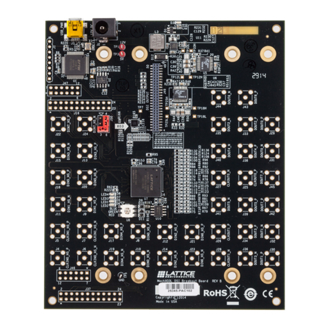
Lattice LatticeECP2 User manual

May 2007
Revision: ebdug18_01.3
LatticeECP2™ Standard Evaluation Board
User’s Guide

2
LatticeECP2 Standard Evaluation Board
Lattice Semiconductor User’s Guide
Introduction
The LatticeECP2 Standard Evaluation Board is a complete, integrated design, featuring a LatticeECP2 FPGA and
a variety of both application-specific and general-purpose peripheral interfaces. This board provides a convenient
platform to evaluate, test, and debug user designs, including designs requiring PCI/PCI-X. This board includes the
following features:
• LatticeECP2 FPGA device in 484 fpBGA package
• SPI Serial Flash device included for low-cost, non-volatile configuration storage
• PCI/PCI-X edge connector (188-pin) supporting Master or Target
– PCI 2.2 - 32/64 bit, 33/66 MHz, 3.3V
– PCI-X - 32/64 bit, 66/133 MHz, parity or ECC, 3.3V (Mode 1)
• RS-232 connector
• 33.33 MHz oscillator
• RJ-45 connector
• LCD connector
• Compact Flash connector
• Prototyping area with access to over 210 I/O pins
• Optional SMA/SMB connectors (up to eight) for high-speed clock and data interfacing
• 7-segment display, eight general purpose switches, two momentary switches, eight user LEDs, and various sta-
tus LEDs
• Required voltages supplied by PCI/PCI-X or one external 5V DC supply
• ispVM
®
System programming support
Figure 1. Lattice ECP2 Standard Evaluation Board
Electrical, Mechanical, and Environmental Specifications
The nominal board dimensions are 9.75 inches by 4.2 inches. The environmental specifications are as follows:
• Operating temperature: 0ºC to 55ºC
• Storage temperature: -40ºC to 75ºC

3
LatticeECP2 Standard Evaluation Board
Lattice Semiconductor User’s Guide
• Humidity: < 95% without condensation
• 5VDC input (+/- 10%) up to 4A, or 3.3V input from PCI/PCI-X backplane
Additional Resources
Additional resources relating to the LatticeECP2 Standard Evaluation Board (including updated documentation,
and sample programs) can be found at the following URL:
www.latticesemi.com/products/developmenthardware/fpgafspcboards/ecp2stardevaluationboard.cfm
Features
LatticeECP2 Device
This board features a LatticeECP2 FPGA with a 1.2V DC core in a 484-ball fpBGA package. A complete descrip-
tion of this device can be found in the LatticeECP2 Family Data Sheet available on the Lattice web site at www.lat-
ticesemi.com/ecp2.
On-Board Oscillator
The 3.3V oscillator socket at Y1 accepts both full-size (14-pin) and half-size (8-pin) oscillators, and will route the
oscillator output to a LatticeECP2 primary clock input or a PLL input, depending on the oscillator’s position in the
socket (see Figure 2).
When a full size oscillator is installed such that pin 1 of the oscillator aligns with pin 1 of the socket, the output of
the oscillator drives the primary clock at LatticeECP2 pin J21 (this is the default position). When pin 1 of the oscilla-
tor is aligned to pin 2 of the socket, the clock is routed to LatticeECP2 pin J21. When using a half size oscillator,
align pin 1 of the oscillator to pin 1 of the socket to drive the primary clock, or align pin 1 of the oscillator to pin 5 of
the socket to drive the PLL. Note that pin 1 of the oscillator is expected to be a no-connect pin.
Figure 2. Oscillator Options
SPI Serial Flash
SPI Serial Flash are available in three package styles, two of those packages, 8-pin SO and 16-pin SO, are sup-
ported by this board. In general, the 8-pin devices support densities up to 16Mb, while the 16-pin devices support
larger densities. The device chosen for inclusion on this board depends on the density of the installed LatticeECP2,
but the SPI Serial Flash will be large enough to allow two bitstreams to be stored simultaneously in order to support
SPIm mode.
3.3V
GND
3.3V
GND
3.3V
PLL Clock
(N21)
Primary Clock
(J21)
GND
Half-Size
33.33 MHz
Full-Size
33.33 MHz
Full-Size
33.33 MHz
3.3V
GND
Half-Size
33.33 MHz
Pin-1
Pin-1 Pin-1
Pin-1Pin-16
Pin-16 Pin-16
Pin-16
PLL Clock
(N21)
Primary Cloc
k
(J21)
PLL Clock
(N21)
Primary Clock
(J21)
PLL Clock
(N21)
Primary Cloc
k
(J21)
Default
Position

4
LatticeECP2 Standard Evaluation Board
Lattice Semiconductor User’s Guide
The 8-pin device footprint is at U4; the 16-pin device footprint is at U5. Only one location can be populated at a
time.
Configuration/Programming Headers
Two programming headers are provided on the evaluation board, providing access to the LatticeECP2 JTAG port
and sysCONFIG™ port. The JTAG connector is a 1x10 header and the sysCONFIG connector is a 2x17 header.
Both the JTAG and the sysCONFIG ports are also provided with loop-through connectors to allow for easy daisy
chaining of multiple boards. With proper jumper selection (see the next section) standard IDC ribbon cable can be
used without the need to swap wires on the cable.
See the Configuring/Programming The Board section of this document for more information on this topic.
The pinouts for these headers are provided in the following tables.
Note: A parallel port ispDOWNLOAD
®
cable is included with each LatticeECP2 Standard Evaluation Board. When
using a parallel port (1x8) ispDOWNLOAD cable, connect pin 1 of the cable to pin 1 of the 1x10 JTAG header. For
more information on the ispDOWNLOAD Cable, see the ispDOWNLOAD Cables Data Sheet available on the Lat-
tice web site at www.latticesemi.com.
Table 1. JTAG Programming Header Pinout
Table 2. JTAG Loop-Through Header Pinout
Function J4 (1x10)
Vcc (3.3V) 1
TDO
1
2
TDI 3
PROGN
1
4
N/C 5
TMS 6
Ground 7
TCK
1
8
DONE 9
INIT Chain
1
10
1. See section below on jumpers.
Function J5 (1x10)
N/C 1
TDO Chain
1
2
TDI Chain
1
3
PROGN
1
4
N/C 5
TMS 6
Ground 7
TCK
1
8
DONE 9
INIT Chain
1
10
1. See section below on jumpers.

5
LatticeECP2 Standard Evaluation Board
Lattice Semiconductor User’s Guide
Table 3. sysCONFIG Header Pinout (J40)
Table 4. sysCONFIG Loop-Through Header Pinout (J41)
JTAG and sysCONFIG Jumpers
There are several JTAG and sysCONFIG cabling options that can be selected using jumpers.
Function Pin Function
CCLK
1 2
Ground
BUSY / SISPI
3 4
D6
DI/D0
1
5 6
Vcc Bank8
D7 / DOUT
1
7 8
INITN
DONE
9 10
PROGRAMN
D7
11 12
Ground
D6
13 14
Ground
D5
15 16
Ground
D4
17 18
Ground
D3
19 20
Ground
D2
21 22
Ground
D1
23 24
Ground
D0
25 26
Ground
CSN
1
27 28
WRITEN
CS1N
1
29 30
CFG0
Vcc Bank8
31 32
CFG1
Ground
33 34
CFG2
1. See section below on jumpers.
Function Pin Function
CCLK 1 2 Ground
N/C 3 4 N/C
DOUT / CSSON 5 6 N/C
N/C 7 8 INITN
DONE 9 10 PROGRAMN
D7 11 12 Ground
D6 13 14 Ground
D5 15 16 Ground
D4 17 18 Ground
D3 19 20 Ground
D2 21 22 Ground
D1 23 24 Ground
D0 25 26 Ground
CSN / N/C
1
27 28 WRITEN
CS1N / N/C
1
29 30 N/C
N/C 31 32 N/C
Ground 33 34 N/C
1. See section below on jumpers.

6
LatticeECP2 Standard Evaluation Board
Lattice Semiconductor User’s Guide
Default Jumpers Settings
This table lists the default settings for all of the jumpers on the LatticeECP2 Standard Evaluation Board. For a com-
plete description of each jumper refer to the next sections.
Table 5. Default Jumper Settings
JTAG Jumpers
Table 6. TDO Chain Jumper
Table 7. TCK Pull-Down
Table 8. PROGRAMN Pin to JTAG
Location Position Location Position
J1 1 to 2 J29 1 to 2
J3 1 to 2 J30
1 to 2
3 to 4
5 to 6
J7 2 to 3 J31 Open
J8 1 to 2 J32 Open
J9 Open J33 1 to 2
J10 Open J34 2 to 3
J11 Open J35 Open
J13 Open J36 Open
J17 1 to 2 J37 1 to 2
J18 1 to 2 J38 Open
J19 Open J39 1 to 2
J22 Open J43
1 to 2
3 to 4
5 to 6
J23 Open J44 1 to 2
J24 Open
Location Position Function Default
J7 1 to 2 Multiple boards, but not the last board in the chain
2 to 3 Single board, or the last board in a chain X
Determines the JTAG TDO path.
Location Position Function Default
J8
1 to 2 Pull-down, 4.7K to ground X
Open No pull-down
There should be only one TCK pull-down on a JTAG chain.
Location Position Function Default
J10 1 to 2 Connects PROGRAMN pin to the JTAG chain
Open Disconnects PROGRAMN pin from JTAG chain X
This jumper is normally not installed.

7
LatticeECP2 Standard Evaluation Board
Lattice Semiconductor User’s Guide
Table 9. INITN Pin to JTAG
sysCONFIG Jumpers
Table 10. CS1N
Table 11. CSN
Table 12. DI/D[0]
Table 13. D[7]/DOUT
Table 14. CSON to CS1N (Loop-Through)
Table 15. CSON to CSN (Loop-Through)
Location Position Function Default
J11 1 to 2 Connects INITN pin to the JTAG chain
Open Disconnects INITN pin from the JTAG chain X
This jumper is normally not installed.
Location Position Function Default
J31
1 to 2 Pulls CS1N high
2 to 3 Pulls CS1N low
Open No pull-up or pull-down on CS1N X
Location Position Function Default
J32
1 to 2 Pulls CSN high
2 to 3 Pulls CSN low
Open No pull-up or pull-down on CSN X
Location Position Function Default
J33
1 to 2 Routes DI to J40-5 to support serial mode X
2 to 3 Routes data bit D[0] to J40-5 for SPIFAST support
Location Position Function Default
J34 1 to 2 Routes D[7] to J40-7 for SPI sysCONFIG support
2 to 3 Routes DOUT to J40-7 to support serial mode X
Location Position Function Default
J35 1 to 2 CSON drives CS1N on the loop-through connector
Open CS1N on the loop-through connector is open X
Location Position Function Default
J36 1 to 2 CSON drives CSN on the loop-through connector
Open CSN on the loop-through connector is open X

8
LatticeECP2 Standard Evaluation Board
Lattice Semiconductor User’s Guide
Table 16. Configuration Mode (J43)
Table 17. SPIFAST
Table 18. Jumper Settings for sysCONFIG Parallel
Table 19. Jumper Settings for sysCONFIG Serial
Configuration
Mode
CFG[2],
1 to 2
CFG[1],
3 to 4
CFG[0],
5 to 6
SPI (default) Jumper (0) Jumper (0) Jumper (0)
Reserved Jumper (0) Jumper (0) Open (1)
SPIm Jumper (0) Open (1) Jumper (0)
Reserved Jumper (0) Open (1) Open (1)
Reserved Open (1) Jumper (0) Jumper (0)
Slave Serial Open (1) Jumper (0) Open (1)
Reserved Open (1) Open (1) Jumper (0)
Slave Parallel Open (1) Open (1) Open (1)
Location Position Function Default
J44
1 to 2 SPI fast read, enables read op-code 0x0B X
Open SPI normal read, enables read op-code 0x03
All SPI Serial Flash shipped with this board support fast read. This jumper must be removed when using the sysCONFIG par-
allel port.
Location Position Notes
J31 Open See schematic
J32 Open See schematic
J33 1 to 2
J34 2 to 3
J43 All Open
J44 Open
J35, J36 Open Bypass Overflow
J35, J36 1 to 2 Flow-through Overflow
Location Position Notes
J31 Open
J32 Open
J33 1 to 2
J34 2 to 3
J43
Open
3 to 4 Open if driven by cable
Open
J44 Don’t Care
J35, J36 Open Bypass Overflow
J35, J36 1 to 2 Not allowed

9
LatticeECP2 Standard Evaluation Board
Lattice Semiconductor User’s Guide
Table 20. Jumper Settings for SPI Emulation via J40
Power Setup
For stand-alone board operation, i.e. outside of a PCI/PCI-X backplane, the evaluation board must be supplied with
a single 5V DC power supply. 5V DC power may be applied using an AC adapter, such as the Condor Electronics
S-5V0-4A0-U11-206IP (or similar), plugged into the power jack at J47, or via the banana jacks at J45 (ground) and
J46 (5V DC).
Table 21. AC Adaptor Specifications
When the board is inserted into a PCI/PCI-X backplane, the on-board 3.3V regulator is automatically disabled; all
onboard power will be derived from the PCI/PCI-X 3.3V power rail.
Additional on-board regulators supply 1.2V, an adjustable voltage, and 5V (for the optional LCD panel). The adjust-
able voltage is set by the potentiometer R36, on the right side of the board, and can be set to any value between
1.22V and 2.5V.
The header at J30 allows a current measuring device to be inserted between 1.2V and the FPGA core. To measure
current remove power from the board, remove all of the jumpers at J30, install a meter between the odd pins and
the even pins, for example between pins 1 and 2, and apply power to the board. When measurement is complete,
remove power from the board and re-install all three jumpers.
Table 22. 1.2V to V
CC
Core
The header at J29 allows a current measuring device to be inserted between 3.3V and the FPGA’s V
CCAUX.
To
measure current, remove power from the board, remove the jumper at J29, install a meter between pins 1 and 2,
and apply power to the board. When measurement is complete, remove power from the board and re-install the
jumper.
Location Position Notes
J31 Open
J32 Open
J33 2 to 3
J34 1 to 2
J43
1 to 2 Open if driven by cable
3 to 4 Open if driven by cable
5 to 6 Open if driven by cable
J44 Open
J35, J36 Open Bypass Overflow
J35, J36 1 to 2 Not allowed
Voltage 5VDC +/- 10%
Current Capacity Up to 4A
Polarity Positive Center
Connector I.D. 0.1” (2.5mm)
Connector O.D. 0.218” (5.5mm)
Location Position Function Default
J30
1 to 2
Connects 1.2V to the FPGA Core
X
3 to 4 X
5 to 6 X
10
LatticeECP2 Standard Evaluation Board
Lattice Semiconductor User’s Guide
Table 23. 3.3V to V
CCAUX
The LatticeECP2 is divided into 10 banks of I/Os (see Table 24), and each of these banks has a separate and inde-
pendent V
CC.
Each bank supports voltages from 1.2V to 3.3V. However, because some banks, such as banks 4
and 5, which connect to PCI/PCI-X, require a fixed voltage, not all of the banks on this evaluation board are adjust-
able. The jumpers listed in Table 24 allow the user to select the voltage (V
CCIO
) applied to the adjustable banks.
Note that if the LatticeECP2 will be configured from the SPI Serial Flash, bank 8 must be set to 3.3V (because SPI
Serial Flash is 3.3V). Also, if the board is plugged into a PCI/PCI-X connector, bank 6 must be set to 3.3V (because
the PCI clock is routed to bank 6 on this board).
Table 24. Bank Voltage Selection
The following tables detail the various I/O standards supported by the LatticeECP2 sysIO™ structures. More infor-
mation can be found in Lattice technical note TN1102,
LatticeECP2 sysIO Usage Guide,
available on the Lattice
web site at www.latticesemi.com.
Table 25. Mixed Voltage I/O Support
For example, if V
CCIO
is 3.3V, then signals from devices powered by 1.2V, 2.5V, or 3.3V can be input and the
thresholds will be correct, assuming the user has also selected the desired input level using ispLEVER
®
software.
Output levels are tied directly to V
CCIO.
Location Position Function Default
J29 1 to 2 Connects 3.3V to VCCAUX X
Bank Function Jumper Settings
0 I/O — 3.3V Only
1 I/O — 3.3V Only
2 I/O J37
1 - 2 = 3.3V
3 - 4 = ADJ
5 - 6 = 1.2V
3 I/O — 3.3V Only
4 I/O — 3.3V Only
5 I/O — 3.3V Only
6 I/O J18
1 - 2 = 3.3V
3 - 4 = ADJ
5 - 6 = 1.2V
7 I/O J17
1 - 2 = 3.3V
3 - 4 = ADJ
5 - 6 = 1.2V
8 sysCONFIG J39
1 - 2 = 3.3V
3 - 4 = ADJ
5 - 6 = 1.2V
V
CCJ
ispJTAG™ — 3.3V Only
J17, 18, 37, and 39 must have no more than one jumper installed.
V
CCIO
Input sysIO Standards Output sysIO Standards
1.2V 1.5V 1.8V 2.5V 3.3V 1.2V 1.5V 1.8V 2.5V 3.3V
1.2V Ye s Ye s Ye s Ye s
1.5V Ye s Ye s Ye s Ye s Ye s
1.8V Ye s Ye s Ye s Ye s Ye s
2.5V Ye s Ye s Ye s Ye s
3.3V Ye s Ye s Ye s Ye s

11
LatticeECP2 Standard Evaluation Board
Lattice Semiconductor User’s Guide
Table 26. sysIO Standards Supported per Bank
PCI/PCI-X
The LatticeECP2 Standard Evaluation Board is designed to be compatible with PCI (PCI SIG 2.2 specification) and
PCI-X (Mode 1). All necessary signals required for 64-bit PCI/PCI-X operation are provided, as shown in Table 27
and Table 28.
Description
Top Side,
Banks 0-1
Right Side,
Banks 2-3
Bottom Side,
Banks 4-5
Left Side,
Banks 6-7
Types of I/O Buffers Single-ended Single-ended and
Differential
Single-ended Single-ended and
Differential
Output Standards
Supported
LVTTL
LVCMOS33
LVCMOS25
LVCMOS18
LVCMOS15
LVCMOS12
SSTL18 Class I, II
SSTL25 Class I, II
SSTL33 Class I, II
HSTL15 Class I
HSTL18_I, II
SSTL18D Class I, II
SSTL25D Class I, II
SSTL33D Class I, II
HSTL15D Class I
HSTL18D Class I, II
PCI33
LVDS25E
1
LVPECL
1
BLVDS
1
RSDS1
LVTTL
LVCMOS33
LVCMOS25
LVCMOS18
LVCMOS15
LVCMOS12
SSTL18 Class I, II
SSTL25 Class I, II
SSTL33 Class I, II
HSTL15 Class I
HSTL18 Class I, II
SSTL18D Class I, II
SSTL25D Class I, II
SSTL33D Class I, II
HSTL15D Class I, II
HSTL18D Class I, II
PCI33
LVDS
LVDS25E1
LVPECL1
BLVDS1
RSDS1
LVTTL
LVCMOS33
LVCMOS25
LVCMOS18
LVCMOS15
LVCMOS12
SSTL18 Class I
SSTL2 Class I, II
SSTL3 Class I, II
HSTL15 Class I
HSTL18 Class I, II
SSTL18D Class I, II
SSTL25D Class I, II,
SSTL33D Class I, II
HSTL15D Class I
HSTL18D Class I, II
PCI33
LVDS25E1
LVPECL1
BLVDS1
RSDS1
LVTTL
LVCMOS33
LVCMOS25
LVCMOS18
LVCMOS15
LVCMOS12
SSTL18 Class I
SSTL2 Class I, II
SSTL3 Class I, II
HSTL15 Class I, III
HSTL18 Class I, II, III
SSTL18D Class I,
SSTL25D Class I, II,
SSTL33D_I, II
HSTL15D Class I
HSTL18D Class I, II
PCI33
LVDS
LVDS25E1
LVPECL1
BLVDS1
RSDS1
Inputs All Single-ended, Differ-
ential
All Single-ended,
Differential
All Single-ended,
Differential
All Single-ended,
Differential
Clock Inputs All Single-ended, Differ-
ential
All Single-ended,
Differential
All Single-ended,
Differential
All Single-ended,
Differential
PCI Support PCI33 no clamp PCI33 no clamp PCI33 with clamp PCI33 no clamp
LVDS Output Buffers LVDS (3.5mA) Buffers2LVDS (3.5mA) Buffers2
1. These differential standards are implemented by using complementary LVCMOS drivers and external resistors.
2. Available on 50% of the I/Os in the Bank.
Table 27. PCI Connections - Solder Side
J48 Signal Name LatticeECP2 Pin sysIO Bank Note
1 PCI_TRSTN - - TP10, PD if master
2 +12V - - Decoupling cap
3 PCI_TMS - - TP11, PU if master
4 PCI_TDI - - TP12, J14-4, J13
5 +5V - - NC
6 PCI_INTA_N - - J19
7 PCI_INTC_N - - J19

12
LatticeECP2 Standard Evaluation Board
Lattice Semiconductor User’s Guide
8 +5V - - NC
9 PCIX_ECC5 W4 5
10 +3.3V - -
11 PCIX_ECC3 W5 5
14 +3.3VAUX - - TP13
15 PCI_RST_N Y4 5
16 +3.3V - -
17 PCI_GNT_N Y5 5
18 GND - -
19 PME# - - TP9
20 PCI_AD30 W6 5
21 3.3V - -
22 PCI_AD28 Y6 5
23 PCI_AD26 W7 5
24 GND - -
25 PCI_AD24 Y7 5
26 PCI_IDSEL U9 5
27 +3.3V - -
28 PCI_AD22 W8 5
29 PCI_AD20 Y8 5
30 GND
31 PCI_AD18 V9 5
32 PCI_AD16 W9 5
33 +3.3V - -
34 PCI_FRAME_N U10 5
35 GND - -
36 PCI_TRDY_N V10 5
37 GND - -
38 PCI_STOP_N W10 5
39 +3.3V - -
40 PCI_SMBCLK - - TP8, PU if master
41 PCI_SMBDAT - - TP14, PU if master
42 GND - -
43 PCI_PAR Y10 5
44 PCI_AD15 W11 5
45 +3.3V - -
46 PCI_AD13 U12 4
47 PCI_AD11 Y12 4
48 GND - -
49 PCI_AD9 W12 4
52 PCI_CBE0_N V12 4
53 +3.3V - -
54 PCI_AD6 U13 4
55 PCI_AD4 Y13 4
Table 27. PCI Connections - Solder Side (Continued)
J48 Signal Name LatticeECP2 Pin sysIO Bank Note

13
LatticeECP2 Standard Evaluation Board
Lattice Semiconductor User’s Guide
56 GND - -
57 PCI_AD2 W13 4
58 PCI_AD0 U14 4
59 +3.3V - -
60 PCI_REQ64_N W14 4
61 NC - -
62 NC - -
63 GND - -
64 PCI_CBE7_N V14 4
65 PCI_CBE5_N U15 4
66 +3.3V - -
67 PAR64 T15 4
68 PCI_AD62 Y15 4
69 GND - -
70 PCI_AD60 W15 4
71 PCI_AD58 U16 4
72 GND - -
73 PCI_AD56 V16 4
74 PCI_AD54 T16 4
75 +3.3V - -
76 PCI_AD52 Y16 4
77 PCI_AD50 W16 4
78 GND - -
79 PCI_AD48 Y17 4
80 PCI_AD46 W17 4
81 GND - -
82 PCI_AD44 Y18 4
83 PCI_AD42 W18 4
84 +3.3V - -
85 PCI_AD40 Y19 4
86 PCI_AD38 Y20 4
87 GND - -
88 PCI_AD36 V17 4
89 PCI_AD34 V18 4
90 GND - -
91 PCI_AD32 U18 4
92 NC - -
93 GND - -
94 NC - -
Note: PD = pull-down resistor, PU = pull-up resistor, NC = no-connect, TP = test point.
Table 27. PCI Connections - Solder Side (Continued)
J48 Signal Name LatticeECP2 Pin sysIO Bank Note

14
LatticeECP2 Standard Evaluation Board
Lattice Semiconductor User’s Guide
Table 28. PCI Connections - Component Side
J14 Signal Name LatticeECP2 Pin sysIO Bank Notes
1 -12V - - Decoupling cap
2 PCI_TCK - - TP16, PD if master
3 GND - -
4 PCI_TDO - - TP17, J3, J13
5 +5V - - NC
6 +5V - - NC
7 PCI_INTB_N - - J19
8 PCI_INTD_N - - J19
9 PCI_PRSNT1_N J14 -
10 PCIX_ECC4 W3 5
11 PCI_PRSNT2_N - - J23
14 PCIX_ECC2 Y2 5
15 GND - -
16 PCI_CLK R1 6 D20, J22
17 GND - -
18 PCI_REQ_N Y3 5
19 +3.3V - -
20 PCI_AD31 AB2 5
21 PCI_AD29 AA3 5
22 GND - -
23 PCI_AD27 AB3 5
24 PCI_AD25 AB4 5
25 3.3V - -
26 PCI_CBE3_N AA5 5
27 PCI_AD23 AB5 5
28 GND - -
29 PCI_AD21 AA6 5
30 PCI_AD19 AB6 5
31 3.3V - -
32 PCI_AD17 AB7 5
33 PCI_CBE2_N AA7 5
34 GND - -
35 PCI_IRDY_N AB8 5
36 +3.3V - -
37 PCI_DEVSEL_N U11 5
38 PCIXCAP - -
39 LOCK# - - TP15
40 PCI_PERR_N AA8 5
41 +3.3V - -
42 PCI_SERR_N AA9 5
43 +3.3V - -
44 PCI_CBE1_N AB9 5
45 PCI_AD14 AA10 5
46 GND - -

15
LatticeECP2 Standard Evaluation Board
Lattice Semiconductor User’s Guide
47 PCI_AD12 AB10 5
48 PCI_AD10 AA11 5
49 PCI_M66EN - - J38
52 PCI_AD8 AB11 5
53 PCI_AD7 Y11 5
54 +3.3V - -
55 PCI_AD5 AB12 5
56 PCI_AD3 AA12 5
57 PCI_GND_57 - - U6
58 PCI_AD1 AB13 5
59 +3.3V - -
60 PCI_ACK64_N AA13 4
61 +5V - - NC
62 +5V - - NC
63 NC - -
64 GND - -
65 PCI_CBE6_N AB14 5
66 PCI_CBE4_N AA14 4
67 GND - -
68 PCI_AD63 AB15 4
69 PCI_AD61 AA15 4
70 +3.3V - -
71 PCI_AD59 AB16 4
72 PCI_AD57 AA16 4
73 GND - -
74 PCI_AD55 AB17 4
75 PCI_AD53 AA17 4
76 GND - -
77 PCI_AD51 AB18 4
78 PCI_AD49 AA18 4
79 +3.3V - -
80 PCI_AD47 AB19 4
81 PCI_AD45 AB20 4
82 GND - -
83 PCI_AD43 AA20 4
84 PCI_AD41 AB21 4
85 GND - -
86 PCI_AD39 AA22 4
87 PCI_AD37 AA21 4
88 +3.3V - -
89 PCI_AD35 Y22 4
90 PCI_AD33 Y21 4
91 GND - -
92 NC - -
Table 28. PCI Connections - Component Side (Continued)
J14 Signal Name LatticeECP2 Pin sysIO Bank Notes

16
LatticeECP2 Standard Evaluation Board
Lattice Semiconductor User’s Guide
PCI/PCI-X Jumpers
Table 29. PRSNT1
Table 30. PRSNT2
Table 31. PCIXCAP and M66EN Encoding
Table 32. PCI TDI and TDO
Table 33. PCI Interrupt
93 NC - -
94 GND - -
Note: PD = pull-down resistor, PU = pull-up resistor, NC = no-connect, TP = test point.
Location Position Function Default
J9
1 to 2 Master PCI/PCI-X
2 to 3 Target PCI/PCI-X
Open Target PCI/PCI-X X
Not installed. If installing header, first cut trace between 2 and 3. If master, also install R51 and C39.
Location Position Function Default
J23 1 to 2 Master PCI/PCI-X
Open Target PCI/PCI-X X
Not installed. If master, also install R62 and C47.
PCIXCAP(J24) M66EN(J38)
Frequency
DefaultPCI PCI-X
1 to 2 2 to 3 33MHz 66MHz
1 to 2 Open 66MHz 66MHz
Open 2 to 3 33MHz 133MHz
Open Open 66MHz 133MHz X
Don’t Care 1 to 2 Master Master
If master, also install R126 and C111.
Location Position Function Default
J13 1 to 2 Target PCI/PCI-X X
Open Master PCI/PCI-X
Not installed. If master then cut the trace between 1 and 2.
Location Position Function Default
J19
2 to 4 INT = INTA X
1 to 3 INT = INTB
4 to 6 INT = INTC
3 to 5 INT = INTD
Not installed. If installing header, first cut trace between 2 and 4.
Table 28. PCI Connections - Component Side (Continued)
J14 Signal Name LatticeECP2 Pin sysIO Bank Notes

17
LatticeECP2 Standard Evaluation Board
Lattice Semiconductor User’s Guide
Table 34. PCI CLK
If the board is to be a master, in addition to properly setting the jumpers, the following resistors and capacitors must
be installed.
Table 35. Install These Resistors and Caps if PCI/PCI-X is a Master
Signal Testing
This board supports testing of single-ended and differential signals.
High-Speed Single-Ended
There are eight FPGA signals that have been routed to special test points on the board. Each signal can include a
series resistor, as well as a pull-up resistor and a pull-down resistor (for maximum flexibility these resistors are not
included with the board). Each series resistor footprint has a shorting trace that must be cut before installing a
resistor (see Figure 3). Next to each signal’s test point a ground point has been added in order to make signal
integrity measurements easier and more accurate.
Figure 3. Resistor Shorting Trace
Table 36. Single Ended SI Test Points
Location Position Function Default
J22 1 to 2
Routes PCI_CLK to FPGA, only used if installing this board in a PCI or
PCI-X backplane. For signal integrity, also remove R27 and R30. D20
provides PCI clamping for this signal.
Open Disconnects this signal from the FPGA X
The differential signals at J20 and J21 can not be used if this jumper is installed (1 to 2).
Location Value Manufacturer Part Number1
R1, 51, 59, 60, 61, 62, 106, 107, 126 5.6K Panasonic ERJ-3GEYJ562V
C39, 111 0.01uF Panasonic ECU-V1H103KBV
1. Or equivalent.
Test Point Pin
Resistors
Series1Pull-Up Pull-Down
TP_SI7 J4 R8 R71 R2
TP_SI6 J5 R9 R72 R3
TP_SI5 L6 R10 R73 R4
TP_SI4 L5 R11 R74 R5
TP_SI3 K2 R12 R75 R6
TP_SI2 K1 R13 R76 R7
TP_SI1 L2 R22 R82 R20
TP_SI0 L1 R23 R83 R21
1. Cut shorting trace before installation.
Cut this trace

18
LatticeECP2 Standard Evaluation Board
Lattice Semiconductor User’s Guide
High-Speed Differential
The board supports testing of up to eight differential pairs using two types of connectors, SMA and RJ45. Each pair
has provision for a “line-to-line” resistor as well as single-ended series resistors (for maximum flexibility these resis-
tors are not included with the board). The resistors can be used as termination or in combination to provide signal
emulation (level shifting). For more information on signal emulation and signal types, please refer to Lattice techni-
cal note number TN1102, LatticeECP2 sysIO Usage Guide, available on the Lattice web site at www.lattices-
emi.com.
Table 37. Differential SI Connectors
Test Points
For GPIO (general purpose I/O) testing or monitoring, numerous test points are provided. The test points are
labeled according to the associated I/O pin location, for example TP_A21. These test points have been arranged in
grids that have grounds and VCCIOs placed nearby to allow for easy prototyping. Please refer the schematics at the
end of this document for more information.
Note that the test points for J21 and N21 have locations for zero ohm resistors (R115 and R117) to allow isolation
of the test points from the oscillator clock. By default these resistors are not installed on the board.
Switches
Switch 1 (SW1) on the top edge of the board is an eight-switch block that is part of the prototyping area. A switch in
the down position produces a low (logic 0), while the up position produces a high (logic 1). All SW1 signals go to
bank 1.
Connector LatticeECP2 Resistors
Location Type Pin Type1Series2Line-to-Line
J27 SMA P1 GDLLT IN R24 R26
J28 P2 GDLLC IN R25
J26 SMA M5 PCLKT IN R84 R86
J25 M6 PCLKC IN R85
J21 SMA R1 GPLLT IN R28 R303
J20 R2 GPLLC IN R29
J15 SMA R3 GPLLT FB R89 R91
J16 T4 GPLLC FB R90
U6-1 RJ45 E2 GPIO R14 R18
U6-2 E1 GPIO R15
U6-3 RJ45 J2 GPIO R16 R19
U6-4 J1 GPIO R17
U6-5 RJ45 K3 GPIO R77 R80
U6-6 K4 GPIO R78
U6-7 RJ45 L4 GPIO R79 R81
U6-8 L3 GPIO R87
1. All support true LVDS.
2. The shorting trace must be cut before installing the resistor.
3. R27 must be installed and J22 must be open if using J21.

19
LatticeECP2 Standard Evaluation Board
Lattice Semiconductor User’s Guide
Table 38. SW1 Connections
SW2 is a momentary switch that, when pressed, forces the FPGA to start a configuration cycle.
SW3 is a momentary switch that the user can define for any purpose, such as a global reset. SW3 is wired to I/O
E18 (bank 1) and applies a low logic level (0) when pressed.
LEDs
Eight user-definable LEDs are provided on the top of the board under SW1. These LEDs are each wired to a sepa-
rate GPIO on bank 1 as defined in the Table 39. The current limiting resistors associated with these LEDs are wired
to 3.3V, but it is safe to drive these signals with any FPGA I/O voltage. The LED will light when its associated I/O pin
is driven low.
Table 39. LED Connections
There are also three LEDs associated with the dedicated programming pins.
Table 40. Programming LEDs
Note: During JTAG programming, the state of the DONE LED has no meaning. This is because the DONE pin,
which drives the LED, is being controlled by the pin’s BSCAN cell. See Lattice technical note number TN1108,
LatticeECP2 sysCONFIG Usage Guide, for more information on the dedicated programming pins.
Seven-Segment Display
This board contains a seven-segment display, with decimal point, at U2. The segments are wired to GPIO as
defined in Table 41. A low on the pin will turn on the associated segment.
Switch Pin
SW1-1 C12
SW1-2 B12
SW1-3 A11
SW1-4 A12
SW1-5 D12
SW1-6 E12
SW1-7 D13
SW1-8 E13
LED Pin
D1 B14
D2 A14
D3 D14
D4 C13
D5 E14
D6 F14
D7 A13
D8 B13
LED Pin Color Function
D12 PROGRAMN Yellow On when signal is low
D11 INITN Red On when initializing
D10 DONE Green On when configuration is complete

20
LatticeECP2 Standard Evaluation Board
Lattice Semiconductor User’s Guide
Table 41. Seven-Segment Display Connections
Figure 4. Seven-Segment Display
LCD Connector
The LCD Connector has 18 pins, but only 16 are required for simple LCD panels. If using an OPTREX 51505 or
equivalent, use pins 1-16, if using a LUMEX LCM-S02002DSR or equivalent, use pins 3-18.
Two potentiometers are provided for LCD control. R34 adjusts the backlight and R35 adjusts the contrast. Power for
the LCD panel is provided by the 3.3V to 5V converter at U7.
Segment Pin
A A15
B A17
C C15
D E15
E F15
F B15
G A16
DP D15
A
G
D
E C
BF
DP
Table of contents
Other Lattice Motherboard manuals

Lattice
Lattice iCE40 UltraPlus User manual

Lattice
Lattice MachXO2280 User manual

Lattice
Lattice ORCA ORT42G5 Instruction Manual

Lattice
Lattice DisplayPort VIP Input Board User manual

Lattice
Lattice Certus-NX Versa User manual

Lattice
Lattice ECP5 User manual

Lattice
Lattice CrossLink LIF-MD6000 Master Link Board - Revision... User manual

Lattice
Lattice Certus-NX User manual

Lattice
Lattice ORCA ORSO42G5 Instruction Manual

Lattice
Lattice iCE40 Ultra User manual