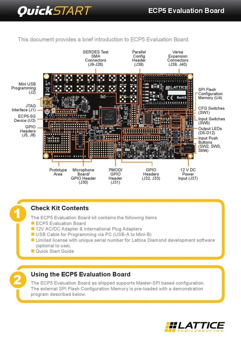
Lattice MachXO2280 User manual

January 2015
EB66_1.1
MachXO2280 Breakout Board Evaluation Kit
User Guide

2
MachXO2280 Breakout Board Evaluation Kit
Introduction
Thank you for choosing the Lattice Semiconductor MachXO™2280 Breakout Board Evaluation Kit!
This user guide describes how to start using the MachXO2280 Breakout Board, an easy-to-use platform for evalu-
ating and designing with the MachXO2280 PLD. Along with the board and accessories, this kit includes a pre-
loaded demonstration design. You may also reprogram the on-board MachXO2280 device to review your own cus-
tom designs.
Note: Static electricity can severely shorten the lifespan of electronic components. See the Storage and Handling
section of this document for handling and storage tips.
Features
The MachXO2280 Breakout Board Evaluation Kit includes:
•MachXO2280 Breakout Board – The board is a 3” x 3” form factor that features the following on-board compo-
nents and circuits:
– MachXO2280 PLD (LCMXO2280C-3FTN256C)
– USB mini-B connector for power and programming
– Eight LEDs
– 40-hole prototype area
– Eight 2x20 expansion header landings for general I/O, JTAG, and external power
– 1x8 expansion header landing for JTAG
– 3.3V supply rail
•Pre-loaded Demo – The kit includes a pre-loaded counter design that highlights use of the embedded
MachXO2280 oscillator and programmable I/Os configured for LED drive.
•USB Connector Cable – The board is powered from the USB mini-B socket when connected to a host PC. The
USB channel also provides a programming interface to the LCMXO2280C JTAG port.
•Lattice Breakout Board Evaluation Kits Web Page – Visit www.latticesemi.com/breakoutboards for the latest
documentation (including this guide), demo designs, and drivers for the kit.
The content of this user guide includes demo operation, programming instructions, top-level functional descriptions
of the Breakout Board, descriptions of the on-board connectors, and a complete set of schematics.

3
MachXO2280 Breakout Board Evaluation Kit
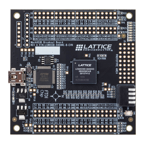
Figure 1. MachXO2280 Breakout Board, Top Side
Left Side
Two 2x20 Header
Landings (J9, J10)
USB
JTAG Header
Landing (J1)
LED
Array
Bottom Side
Two 2x20 Header Landings (J7 & J8)
Top Side
Two 2x20 Header Landings (J3 & J4 )
Right Side
Two 2x20 Header Landings
(J5 & J6)
Prototype
Area
Storage and Handling
Static electricity can shorten the lifespan of electronic components. Please observe these tips to prevent damage
that could occur from electro-static discharge:
• Use anti-static precautions such as operating on an anti-static mat and wearing an anti-static wrist-band.
• Store the evaluation board in the packaging provided.
• Touch a metal USB housing to equalize voltage potential between you and the board.
Software Requirements
You should install the following software before you begin developing new designs for the Breakout board:
• FTDI Chip USB Hardware Drivers
•Lattice Diamond™ (MachXO support)
• ispVM System™ 17.9 or later (Required for re-programming)
MachXO2280 Device
This board features the MachXO2280 PLD which offers the benefits of increased system integration by providing
over 27Kbits of embedded memory, two built-in PLLs, high performance LVDS I/Os, and a low power sleep mode,
all in a single-device. The 256-pin ftBGA package provides 211 user I/Os in a 17mm x 17mm package. A complete
description of this device can be found in DS1002, MachXO Family Data Sheet.

4
MachXO2280 Breakout Board Evaluation Kit
Demonstration Design
Lattice provides a pre-programmed demo to illustrate basic operation of the MachXO2280 device. The design inte-
grates an up-counter with the on-chip oscillator.
Note: You may obtain your Breakout Board after it has been reprogrammed. To restore the factory default demo
and program it with other Lattice-supplied examples see the Download Demo Designs section of this document.
Run the Demonstration Design
The preprogrammed demonstration design is an up-counter to drive an LED array. The program shows a clock
generator based on the MachXO2280 on-chip oscillator. The counter module is clocked at ~22 MHz (18-26MHz) to
illustrate how low speed timer functions can be implemented with a PLD. The 23-bit up-counter further divides the
clock to advance the LED display approximately every 200ms. The resulting light pattern will appear as an alternat-
ing pair of lit LEDs per row.
Figure 2. Counter Demo Block Diagram
2x4 LED
Array
MachXO2280
23-bit
Up-Counter
Clock
Generator 18-26 MHz
c_delay[22:0]
c_delay[22]
(~0.5Hz)
WARNING: Do not connect the Breakout Board to your PC before you follow the driver installation procedure of
this section.
Communication with the Breakout Board with a PC via the USB connection cable will require the FTDI chip USB
hardware drivers contained in the Software Requirements section. Loading these drivers enables the computer to
reliably recognize and program the Breakout Board. Drivers are distributed by Lattice as a stand-alone package or
with ispVM System version 17.9 or later. Use one of the two procedures below to install.
To load the FTDI chip USB hardware drivers via ispVM System:
1. Browse to www.latticesemi.com/breakoutboards and download ispVM System software.
2. Install ispVM System software.
3. Run ispVM System. Choose ispTools > Install/Uninstall LSC USB/Parallel Port Driver.
The LSC 32/64-Bit USB Drivers Install/Uninstall dialog appears.
4. Select FTDI USB 32-Bit Driver or FTDI USB 64-Bit Driver then click Install.
After a few moments, ispVM will indicate the installation is complete.
5. Click OK, then click Close from the LSC 32/64-Bit USB Drivers Install/Uninstall dialog.
6. Choose File > Exit to close ispVM System.
7. Connect the USB cable from a USB port on your PC to the board’s USB mini-B socket (J2). After connection is
made, a green Power LED (D9) will light indicating the board is powered on.
8. Red LEDs will light and start to flash according to the preprogrammed demonstration design.
See the Troubleshooting section of this guide if the board does not function as expected.

5
MachXO2280 Breakout Board Evaluation Kit
To load the FTDI chip USB hardware drivers via the stand-alone package:
1. Browse to www.latticesemi.com/breakoutboards and download the FTDI chip USB Hardware driver package.
2. Extract the FTDI chip USB Hardware driver package to your PC hard drive.
3. Connect the USB cable from a USB port on your PC to the board’s USB mini-B socket (J2). After connection is
made, a green Power LED (D9) will light indicating the board is powered on.
4. If you are prompted, “Windows may connect to Windows Update” select No, not this time from available
options and click Next to proceed with the installation. Choose the Install from specific location (Advanced)
option and click Next.
5. Search for the best driver in these locations and click the Browse button to browse to the Windows driver folder
created in the Download Windows USB Hardware Drivers section. Select the CDM 2.04.06 WHQL Certified
folder and click OK.
6. Click Next. A screen will display as Windows copies the required driver files. Windows will display a message
indicating that the installation was successful.
7. Click Finish to install the USB driver.
8. Red LEDs will light and start to flash according to the preprogrammed demonstration design.
See the Troubleshooting section of this guide if the board does not function as expected.
Download Demo Designs
The counter demo is preprogrammed into the Breakout Board, however over time it is likely your board will be mod-
ified. Lattice distributes source and programming files for demonstration designs compatible with the Breakout
Board.
To download demo designs:
1. Browse to the Lattice Breakout Board Evaluation Kits web page (www.latticesemi.com/breakoutboards) of the
Lattice web site. Select MachXO Breakout Board Demo Source and save the file.
2. Extract the contents of MachXO2280_BB_Eval_Kit_v01.0.zip to an accessible location on your hard drive.
The demo design directory Demo_LED is unpacked.
Recompile a Demonstration Project with Lattice Diamond
Use the procedure described below to recompile a demo project for the Breakout Board.
1. Install and license Lattice Diamond software.
2. Download the demo source files from the Lattice Breakout Board Evaluation Kits web page.
3. Run Lattice Diamond.
4. Open the Demo_LED_OSC.ldf project file.
5. From the Process view, select JEDEC File from the Export Files process.
6. Choose Export Files, right-click and choose Run.
After a few moments the JEDEC programming file is output.
7. See section the Programming with ispVM section for details on downloading a programming file to the board.
6
MachXO2280 Breakout Board Evaluation Kit
Programming with ispVM
A demonstration design is pre-programmed into the Breakout Board by Lattice. To restore a Breakout Board to fac-
tory settings or load an alternative demo design, use the procedures in this section.
To install ispVM programming tools:
1. Install and license ispVM System software.
2. Connect the board to a host PC using the USB port header connection.
3. Follow the USB Cable Interface procedure below to program the evaluation board.
The Breakout Board is equipped with a built-in USB-based programming circuit. This consists of a USB PHY and a
USB connector. When the board is connected to a PC with a USB cable, it is recognized by the ispVM System soft-
ware as a USB Download Cable. The MachXO2280 can then be scanned and programmed using the ispVM Sys-
tem software.
To program a demo programming file:
1. From the Start menu run ispVM System.
ispVM appears.
2. Choose Options > Cable and IO Port Setup…
The Cable and I/O Port Setup dialog appears.
3. Make the following selections:
Cable Type: USB2
Port Setting: FTUSB-0
Click OK.
4. Choose ispTools > Scan Chain.
The New Scan Configuration Setup window appears. The LCMXO2280C device appears in the device list.
5. Right-click the LCMXO2280C entry and choose Edit Device…
The Device Information dialog appears.
6. From the Data File section, click the Browse button.
The Open Data File dialog appears.
7. Browse to the <Demo Dir> folder, select <Demo>.jed, and click Open. From the Operation list choose Erase,
Program, Verify and click OK.
8. Choose Project > Download.
ispVM reprograms the evaluation board.
Programming requires about 10 seconds. A small timer window will appear to show elapsed programming time. At
the end of programming, the configuration setup window should show a PASS in the Status column.

7
MachXO2280 Breakout Board Evaluation Kit
MachXO2280 Breakout Board
This section describes the features of the MachXO2280 Breakout Board in detail.
Overview
The Breakout Board is a complete development platform for the MachXO2280 PLD. The board includes a prototyp-
ing area, a USB program/power port, an LED array, and header landings with electrical connections to most of the
PLD’s programmable I/O, power, and JTAG pins. The board is powered by the PC’s USB port or optionally with
external power. You may create or modify the program files using Diamond software and reprogram the board
using ispVM software.
Figure 3. MachXO2280 Breakout Board Block Diagram
LCMXO2280C
-3FTN256C
2x20 Header
Landing (J9)
LED
Array
GPIO
USB
Controller
USB Mini B
Socket
A/Mini-B
USB Cable JTAG
Programming 8
2x20 Header
Landing (J10)
GPIO
2x20 Header
Landing (J5)
GPIO
2x20 Header
Landing (J6)
GPIO
1x8 JTAG Header
Landing (J1)
8
2x20 Header
Landing (J7)
2x20 Header
Landing (J8)
Bank 2,3
Bank 4,5
Bank 0,1
2x20 Header
Landing (J3)
2x20 Header
Landing (J4)
Bank 6,7
GPIOGPIO
GPIO GPIO

8
MachXO2280 Breakout Board Evaluation Kit
Table 1 describes the components on the board and the interfaces it supports.
Table 1. Breakout Board Components and Interfaces
Component/Interface Type
Schematic
Reference Description
Circuits
USB Controller Circuit U2: FT2232H USB-to-JTAG interface and dual USB UART/FIFO IC
USB Mini-B Socket I/O J1:USB_MINI_B Programming and debug interface
Components
LCMXO2280C PLD U4: LCMXO2280C-
3FTN256C 2280-LUT device packaged in a 17 x 17mm, 256-ball ftBGA.
Interfaces
LED Array Output D8-D1 Red LEDs
Eight 2x20 Header
Landings I/O
J3: header_2x20
J4: header_2x20
J5: header_2x20
J6: header_2x20
J7: header_2x20
J8: header_2x20
J9: header_2x20
J10: header_2x20
User-definable I/O
1x8 Header Landing I/O J1: header_1x8 Optional JTAG interface
4-Hole Prototype Area Prototype area 100mil centered holes.

9
MachXO2280 Breakout Board Evaluation Kit
Subsystems
This section describes the principle sub systems for the Breakout Board in alphabetical order.
Clock Sources
All clocks for the counter demonstration designs originate from the MachXO2280 PLD on-chip oscillator. You may
use an expansion header landing to drive a PLD input with an external clock source.
Expansion Header Landings
The expansion header landings provide access to user GPIOs, primary inputs, clocks, and VCCO pins of the
MachXO2280. The remaining pins serve as power supplies for external connections. Each landing is configured as
one 2x20 100 mil.
Table 2. Expansion Connector Reference
Item Description
Reference Designators J3, J4, J5, J6, J7, J8, J9, J10
Part Number header_2x20
Table 3. Expansion Header Pin Information (J3)
Pin Number Function MachXO2280 Ball
1PL2A_LV_T E4
2PL11A_LV_T H2
3PL2B_LV_T E5
4PL11B_LV_C J2
5GND n/a
6GND n/a
7PL3A_LV_T F5
8PL12A_LV_T J1
9PL3B_LV_C F6
10 PL12B_LV_C K1
11 GND n/a
12 GND n/a
13 PL4A_LV_T E3
14 PL13A_LV_T L1
15 PL4B_LV_C E2
16 PL13B_LV_C M1
17 GND n/a
18 GND n/a
19 PL5A_LV_T B1
20 PL15A_LV_T L3
21 PL5B_LV_C C1
22 PL15B_LV_C M3
23 GND n/a
24 GND n/a
25 PL7A_LV_T F2
26 PL16A_LV_T J4
27 PL7B_LV_C G2
28 PL16B_LV_C J5

10
MachXO2280 Breakout Board Evaluation Kit
29 GND n/a
30 GND n/a
31 PL8A_LV_T G4
32 PL17A_LV_T K5
33 PL8B_LV_C G5
34 PL17B_LV_C K4
35 GND n/a
36 GND n/a
37 PL9A_LV_T H4
38 PL18A_LV_T M5
39 PL9B_LV_C H5
40 PL18B_LV_C M4
Pin Number Function MachXO2280 Ball

11
MachXO2280 Breakout Board Evaluation Kit
Table 4. Expansion Header Pin Information (J4)
Pin Number Function MachXO2280 Ball
1PL3C F3
2GND n/a
3PL3D F4
4GND n/a
5PL4C C3
6GND n/a
7PL4D C2
8GND n/a
9PL6C D2
10 GND n/a
11 PL6D D1
12 GND n/a
13 PL7C E1
14 GND n/a
15 PL7D F1
16 GND n/a
17 PL8C G3
18 GND n/a
19 PL8D H3
20 GND n/a
21 PL10C G1
22 GND n/a
23 PL10D H1
24 GND n/a
25 NC NC
26 PL15C M2
27 NC NC
28 PL15D N2
29 PL11C J3
30 PL16C R1
31 PL11D K3
32 PL16D R2
33 PL12C K2
34 PL17C L5
35 PL12D L2
36 PL17D L4
37 PL14C N1
38 PL19A N4
39 PL14D P1
40 PL19B N3

12
MachXO2280 Breakout Board Evaluation Kit
Table 5. Expansion Header Pin Information (J5)
Pin Number Function MachXO2280 Ball
1PT2C B2
2PT9A D8
3PT2D B3
4PT9C E8
5PT3A A2
6PT9D E9
7PT3B A3
8PT10A A10
9PT3C D3
10 PT10C C9
11 PT3D D4
12 PT10D C10
13 PT4A C4
14 PT10E D9
15 PT4B C5
16 PT10F D10
17 PT5A D6
18 PT11A B9
19 PT5B D5
20 PT11B B10
21 PT5C B4
22 PT12A A11
23 PT5D B5
24 PT12B A12
25 PT6E E7
26 PT12C B11
27 PT6F E6
28 PT12D B12
29 PT6C A5
30 PT13C C11
31 PT6D A4
32 PT13D C12
33 PT6A C6
34 PT14A A13
35 PT6B C7
36 PT14B A14
37 PT7A B6
38 PT14C D11
39 PT7B B7
40 PT14D D12

13
MachXO2280 Breakout Board Evaluation Kit
Table 6. Expansion Header Pin Information (J6)
Pin Number Function MachXO2280 Ball
1VCIO_extB7 G6
2GND n/a
3VCIO_extB6 J6
4GND n/a
5VCIO_extB5 L7
6GND n/a
7VCIO_extB4 L9
8GND n/a
9VCIO_extB3 J11
10 GND n/a
11 VCIO_extB2 G11
12 GND n/a
13 VCIO_extB1 F9
14 GND n/a
15 VCIO_extB0 F7
16 GND n/a
17 NC NC
18 NC NC
19 NC NC
20 NC NC
21 NC NC
22 PT15A E10
23 NC NC
24 PT15B E11
25 NC NC
26 PT15C B13
27 NC NC
28 PT15D C13
29 PT7C A6
30 PT16A B14
31 PT7D A7
32 PT16B C14
33 PT8C B8
34 PT16C A15
35 PT8D C8
36 PT16D B15
37 NC NC
38 GND n/a
39 NC NC
40 GND n/a

14
MachXO2280 Breakout Board Evaluation Kit
Table 7. Expansion Header Pin Information (J7)
Pin Number Function LCMXO2280C Ball
1PR4C F13
2GND n/a
3PR4D F12
4GND n/a
5PR5C B16
6GND n/a
7PR5D C16
8GND n/a
9PR6C D16
10 GND n/a
11 PR6D E16
12 GND n/a
13 PR7C F16
14 GND n/a
15 PR7D G16
16 GND n/a
17 PR9C H12
18 GND n/a
19 PR9D H13
20 GND n/a
21 PR10C G15
22 GND n/a
23 PR10D H15
24 GND n/a
25 NC NC
26 PR15C M16
27 NC NC
28 PR15D N16
29 PR11C J12
30 PR16C L12
31 PR11D K12
32 PR16D L13
33 PR13C J14
34 PR17C M12
35 PR13D K14
36 PR17D M13
37 PR14C K16
38 PR20A L11
39 PR14D L16
40 PR20B M11

15
MachXO2280 Breakout Board Evaluation Kit
Table 8. Expansion Header Pin Information (J8)
Pin Number Function MachXO2280 Ball
1PR3A_LV_T D14
2PR11A_LV_T H16
3PR3B_LV_C D13
4PR11B_LV_C J16
5GND n/a
6GND n/a
7PR4A_LV_T E13
8PR13A_LV_T J15
9PR4B_LV_C E12
10 PR13B_LV_C K15
11 GND n/a
12 GND n/a
13 PR5A_LV_T E14
14 PR14A_LV_T J13
15 PR5B_LV_C F14
16 PR14B_LV_C K13
17 GND n/a
18 GND n/a
19 PR6A_LV_T C15
20 PR15A_LV_T L15
21 PR6B_LV_C D15
22 PR15B_LV_C M15
23 GND n/a
24 GND n/a
25 PR7A_LV_T E14
26 PR16A_LV_T L14
27 PR7B_LV_C F15
28 PR16B_LV_C M14
29 GND n/a
30 GND n/a
31 PR9A_LV_T G12
32 PR17A_LV_T N15
33 PR9B_LV_C G13
34 PR17B_LV_C N14
35 GND n/a
36 GND n/a
37 PR10A_LV_T G14
38 PR18A_LV_T N13
39 PR10B_LV_C H14
40 PR18B_LV_C N12

16
MachXO2280 Breakout Board Evaluation Kit
Table 9. Expansion Header Pin Information (J9)
Pin Number Function MachXO2280 Ball
1VCC_3.3V n/a
2GND n/a
3VCC_3.3V n/a
4GND n/a
5VCC_3.3V n/a
6GND n/a
7NC NC
8GND n/a
9NC NC
10 VCC_CORE n/a
11 CLK0 (PT9B) D7
12 GND n/a
13 CLK1 (PT10B) A9
14 GND n/a
15 CLK2 (PB10F) N9
16 GND n/a
17 CLK3 (PB10B) M9
18 GND n/a
19 NC NC
20 NC NC
21 NC NC
22 NC NC
23 SLEEPN P13
24 GND n/a
25 PB14D R14
26 GND n/a
27 PB15A T14
28 GND n/a
29 PB15B T15
30 GND n/a
31 PB15D P14
32 GND n/a
33 PB16A R15
34 GND n/a
35 PB16B R16
36 GND n/a
37 PB16C P15
38 GND n/a
39 PB16D P16
40 GND n/a

17
MachXO2280 Breakout Board Evaluation Kit
Table 10. Expansion Header Pin Information (J10)
Pin Number Function MachXO2280 Ball
1PB9B P8
2PB2A P2
3PB9A P7
4PB2B P3
5PB10E N8
6PB2C N5
7PB10C P9
8PB2D N6
9PB10D P10
10 PB3A T2
11 PB10A M10
12 PB3B T3
13 PB11C R9
14 PB3C R4
15 PB11D R10
16 PB3D R5
17 PB12A T10
18 PB4A P5
19 PB12B T11
20 PB4B P6
21 PB12C N10
22 PB4C T5
23 PB12D N11
24 PB4D T4
25 PB13A R11
26 PB5A R6
27 PB13B R12
28 PB5B T6
29 PB13C P11
30 PB6A T8
31 PB13D P12
32 PB6B T7
33 PB14A T13
34 PB7C M7
35 PB14B T12
36 PB7D M8
37 PB14C R13
38 PB8C R7
39 NC NC
40 PB8D R8

18
MachXO2280 Breakout Board Evaluation Kit
Figure 4. J3/J4 Header Landing Callout
1
E4
E5
GND
F5
F6
GND
E3
E2
GND
B1
C1
GND
F2
G2
GND
G4
G5
GND
H4
H5
39
2
H2
J2
GND
J1
K1
GND
L1
M1
GND
L3
M3
GND
J4
J5
GND
K5
K4
GND
M5
M4
40
1
F3
F4
C3
C2
D2
D1
E1
F1
G3
H3
G1
H1
NC
NC
J3
K3
K2
L2
N1
PI
39
2
GND
GND
GND
GND
GND
GND
GND
GND
GND
GND
GND
GND
M2
N2
R1
R2
L5
L4
N4
N3
40
J3 J4
J3
J4
Top Side
Figure 5. J5/J6 Header Landing Callout
J6 J5
Top Side
1
G6
J6
L7
L9
J11
G11
F9
F7
NC
NC
NC
NC
NC
NC
A6
A7
B8
C8
NC
NC
39
2
GND
GND
GND
GND
GND
GND
GND
GND
NC
NC
E10
E11
B13
C13
B14
C14
A15
B15
GND
GND
40
1
B2
B3
A2
A3
D3
D4
C4
C5
D6
D5
B4
B5
E7
E6
A5
A4
C6
C7
B6
B7
39
2
D8
E8
E9
A10
C9
C10
D9
D10
B9
B10
A11
A12
B11
B12
C11
C12
A13
A14
D11
D12
40
J6 J5

19
MachXO2280 Breakout Board Evaluation Kit
Figure 6. J7/J8 Header Landing Callout
J8
J7
Top Side
1
D14
D13
GND
E13
E12
GND
E14
F14
GND
C15
D15
GND
E14
F15
GND
G12
G13
GND
G14
H14
39
2
H16
J16
GND
J15
K15
GND
J13
K13
GND
L15
M15
GND
L14
M14
GND
N15
N14
GND
N13
N12
40
1
F13
F12
B16
C16
D16
E16
F16
G16
H12
H13
G15
H15
NC
NC
J12
K12
J14
K14
K16
L16
39
2
GND
GND
GND
GND
GND
GND
GND
GND
GND
GND
GND
GND
M16
N16
L12
L13
M12
M13
L11
M11
40
J8 J7
Figure 7. J9/J10 Header Landing Callout
J9 J10
Top Side
1
VCC_3.3 V
VCC_3.3 V
VCC_3.3 V
NC
NC
D7
A9
N9
M9
NC
NC
P13
R14
T14
T15
P14
R15
R16
P15
P16
39
2
GND
GND
GND
VCC_CORE
GND
GND
GND
GND
GND
NC
NC
GND
GND
GND
GND
GND
GND
GND
GND
GND
40
1
P8
P7
N8
P9
P10
M10
R9
R10
T10
T11
N10
N11
R11
R12
P11
P12
T13
T12
R13
NC
39
2
P2
P3
N5
N6
T2
T3
R4
R5
P5
P6
T5
T4
R6
T6
T8
T7
M7
M8
R7
R8
40
J9 J10

20
MachXO2280 Breakout Board Evaluation Kit
Figure 8. J1 Header Landing and LED Array Callout
J1
Top Side
LED
1
VCC3FT
NC
NC
TCK
TDI
TDO
TMS
GND
8
D1
IO_J12
IO_J10
IO_I12
IO_I10
D4
D5
IO_18
IO_16
IO_14
IO_12
D8
J9
MachXO2280 PLD
The LCMXO2280C-3FTN256C is a 256-ball BGA package PLD device which provides 211 I/Os in a 17 x 17mm
package.
Table 11. MachXO PLD Interface Reference
Item Description
Reference Designators U4
Part Number LCMXO2280C-3FTN256C
Manufacturer Lattice Semiconductor
Web Site www.latticesemi.com
JTAG Interface Circuits
For power and programming an FTDI USB UART/FIFO IC converter provides a communication interface between a
PC host and the JTAG programming chain of the Breakout Board. The USB 5V supply is also used as a source for
the 3.3V supply rail. A USB mini-B socket is provided for the USB connector cable.
Table of contents
Other Lattice Motherboard manuals

Lattice
Lattice DisplayPort VIP Input Board User manual

Lattice
Lattice ECP5 User manual

Lattice
Lattice LatticeECP2 User manual

Lattice
Lattice ORCA ORT42G5 Instruction Manual

Lattice
Lattice iCE40 UltraPlus 8:1 Mic Aggregation Demo User manual

Lattice
Lattice iCE40 UltraPlus User manual

Lattice
Lattice iCE40 Ultra User manual

Lattice
Lattice CrossLink LIF-MD6000 Master Link Board - Revision... User manual

Lattice
Lattice LCMXO3L-DSI-EVN User manual

Lattice
Lattice iCEblink40-HX1K User manual