Lattice Certus-NX User manual

Certus-NX Versa Evaluation Board Demo
User Guide
FPGA-UG-02133-1.1
November 2021

Certus-NX Versa Evaluation Board Demo
User Guide
© 2021 Lattice Semiconductor Corp. All Lattice trademarks, registered trademarks, patents, and disclaimers are as listed at www.latticesemi.com/legal.
All other brand or product names are trademarks or registered trademarks of their respective holders. The specifications and information herein are subject to change without notice.
2 FPGA-UG-02133-1.1
Disclaimers
Lattice makes no warranty, representation, or guarantee regarding the accuracy of information contained in this document or the suitability of its
products for any particular purpose. All information herein is provided AS IS, with all faults and associated risk the responsibility entirely of the Buyer.
Buyer shall not rely on any data and performance specifications or parameters provided herein. Products sold by Lattice have been subject to limited
testing and it is the Buyer's responsibility to independently determine the suitability of any products and to test and verify the same. No Lattice
products should be used in conjunction with mission- or safety-critical or any other application in which the failure of Lattice’s product could create a
situation where personal injury, death, severe property or environmental damage may occur. The information provided in this document is
proprietary to Lattice Semiconductor, and Lattice reserves the right to make any changes to the information in this document or to any products at
any time without notice.

Certus-NX Versa Evaluation Board Demo
User Guide
© 2021 Lattice Semiconductor Corp. All Lattice trademarks, registered trademarks, patents, and disclaimers are as listed at www.latticesemi.com/legal.
All other brand or product names are trademarks or registered trademarks of their respective holders. The specifications and information herein are subject to change without notice.
FPGA-UG-02133-1.1 3
Contents
Acronyms in This Document.................................................................................................................................................5
1. Introduction..................................................................................................................................................................6
1.1. Learning Objectives.............................................................................................................................................6
1.2. Linux Version of this Demo .................................................................................................................................6
2. Hardware and Software Requirements........................................................................................................................7
2.1. Hardware Requirements.....................................................................................................................................7
2.2. Software Requirements ......................................................................................................................................7
3. Setting Up the Demo ....................................................................................................................................................8
3.1. Hardware Setup ..................................................................................................................................................8
3.1.1. Installing Hardware into a Different Slot........................................................................................................8
3.2. Software Setup....................................................................................................................................................9
3.2.1. Installing the Drivers on the Host Machine....................................................................................................9
3.2.2. Editing bcdedit.exe.......................................................................................................................................13
3.3. Software Setup on a Linux Machine..................................................................................................................14
3.3.1. Building the User Interface Demo in Linux...................................................................................................14
3.4. Programming the Demo .bit File to the Certus-NX Versa Evaluation Board.....................................................15
4. Running PCIe Basic Demo...........................................................................................................................................18
5. Running PCIe Memory Access Demo..........................................................................................................................20
6. Rebuilding the Demo..................................................................................................................................................21
7. Regenerating the .bit File and Reprogramming the Board.........................................................................................22
8. Troubleshooting .........................................................................................................................................................23
Technical Support Assistance .............................................................................................................................................24
Revision History..................................................................................................................................................................25

Certus-NX Versa Evaluation Board Demo
User Guide
© 2021 Lattice Semiconductor Corp. All Lattice trademarks, registered trademarks, patents, and disclaimers are as listed at www.latticesemi.com/legal.
All other brand or product names are trademarks or registered trademarks of their respective holders. The specifications and information herein are subject to change without notice.
4 FPGA-UG-02133-1.1
Figures
Figure 3.1. Welcome Screen.................................................................................................................................................9
Figure 3.2. Select Destination Folder..................................................................................................................................10
Figure 3.3. Confirm Install...................................................................................................................................................10
Figure 3.4. Device Driver Install Wizard..............................................................................................................................11
Figure 3.5. Windows Security .............................................................................................................................................11
Figure 3.6. Driver Installation Completed Successfully.......................................................................................................12
Figure 3.7. Correct Windows CMD Prompt ........................................................................................................................13
Figure 3.8. Correct Windows CMD Prompt ........................................................................................................................13
Figure 3.9. Radiant Programmer New Project....................................................................................................................15
Figure 3.10. Main Interface ................................................................................................................................................15
Figure 3.11. Device Properties............................................................................................................................................16
Figure 3.12. Programming Button ......................................................................................................................................16
Figure 4.1. Device Info after Correct Software and Hardware Installation ........................................................................18
Figure 4.2. User Interface Control of 7-Segment Display ...................................................................................................19
Figure 4.3. Onboard 7-Segment Display .............................................................................................................................19
Figure 5.1. Memory Access Tab in GUI...............................................................................................................................20
Figure 7.1. Proper Project Properties Configuration ..........................................................................................................22
Tables
Table 3.1. List of Jumpers to be Set for Programming..........................................................................................................8

Certus-NX Versa Evaluation Board Demo
User Guide
© 2021 Lattice Semiconductor Corp. All Lattice trademarks, registered trademarks, patents, and disclaimers are as listed at www.latticesemi.com/legal.
All other brand or product names are trademarks or registered trademarks of their respective holders. The specifications and information herein are subject to change without notice.
FPGA-UG-02133-1.1 5
Acronyms in This Document
A list of acronyms used in this document.
Acronym
Definition
PCIe
Peripheral Component Interconnect Express
SPI
Serial Peripheral Interface

Certus-NX Versa Evaluation Board Demo
User Guide
© 2021 Lattice Semiconductor Corp. All Lattice trademarks, registered trademarks, patents, and disclaimers are as listed at www.latticesemi.com/legal.
All other brand or product names are trademarks or registered trademarks of their respective holders. The specifications and information herein are subject to change without notice.
6 FPGA-UG-02133-1.1
1. Introduction
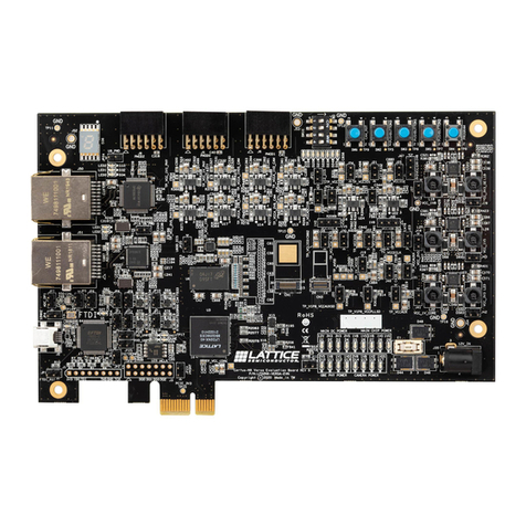
This guide describes how to start using the Certus™-NX Versa Evaluation Board, a low-cost platform for demonstrating
the PCI Express® reference design and for evaluating solutions for your specific application.
The Certus-NX Versa Evaluation Board features the Certus-NX FPGA in the 256-ball caBGA package, which is built on
the Lattice Nexus™ FPGA platform using low power 28 nm FDSOI technology. The board can expand the usability of the
Certus-NX FPGA with DDR3, soft D-PHY, 1 Gbps Ethernet and 1× PCIe (Gen2) channel. Board resources such as jumpers,
LED indicator, push button, and switch are available for user-defined applications.
This guide familiarizes you with the process of setting up your PCI Express development environment. It is assumed
that you do not have any associated tools installed on your system.
The demos discussed in this document include the PCI Express Basic Demo and PCI Express Memory Access Demo.
1.1. Learning Objectives
After completing the steps in this guide, you will be able to perform the following:
Set up the Certus-NX Versa Evaluation Board and become familiar with its main features
Install all applicable development tools and PCI Express demos
Establish communication between the Certus-NX Versa Evaluation Board through the PCI Express link
Run the PCI Express Basic Demo that allows you to control a 7 segment LED on the Certus-NX Versa Evaluation
Board. This demo is included in the user interface.
Run the PCIe Memory Access Demo, which allows you to manipulate the onboard memory of the FPGA through
the PCIe slot. This demo is included in the user interface.
Use what the demo teaches you about designing Lattice PCI Express solutions.
Modify and rebuild the PCI Express Basic Demo.
Become familiar with the software development tools and major design flow steps employed in this kit.
Use other existing documentation in conjunction with this guide.
This document assumes that you have already installed the Lattice Radiant™design software. This document covers
some of the basic of function of Lattice Radiant. If you would like to learn more about Lattice Radiant, refer to the
Radiant Help system.
1.2. Linux Version of this Demo
On the Lattice Semiconductor website, you can download an archive of the files needed to run this demo on Ubuntu
18.04.6 LTS. The steps necessary to complete the Linux version of this demo are provided in the Software Setup on a
Linux Machine section.
Certus-NX Versa Evaluation Board Demo
User Guide
© 2021 Lattice Semiconductor Corp. All Lattice trademarks, registered trademarks, patents, and disclaimers are as listed at www.latticesemi.com/legal.
All other brand or product names are trademarks or registered trademarks of their respective holders. The specifications and information herein are subject to change without notice.
FPGA-UG-02133-1.1 7
2. Hardware and Software Requirements
2.1. Hardware Requirements
To install the kit design and run the demo software, a single computer with a PCI Express ×16, ×8, ×4, or ×1 slot is
required. You must also have a power USB port. All other hardware and drivers are included in the kit.
USB Cable
12 V Power Adapter
Bit file for the Certus-NX board SPI Flash (LFD2NX40_PCIe_Basic_Demo_impl_1.bit)
Lattice Radiant Programmer Software (version 2.2 or later)
http://www.latticesemi.com/Products/DesignSoftwareAndIP/FPGAandLDS/Radiant
Windows 10 (use WDF 1.25 or earlier)
setup.exe file for installing drivers and launching the user interface
2.2. Software Requirements
The following are the software required to obtain the expected results for the procedures described in this guide:
Lattice Radiant 2.2 Programmer or later
Lattice Radiant can be obtained from the Lattice Radiant web page
Certus-NX Basic Demo for Windows 10
Minimum system requirements as described in the Radiant Installation Guide to develop PCI Express designs
Note: Depending on your system, all the files and dependencies for the Certus-NX Basic Demo are available in the .zip
folder.

Certus-NX Versa Evaluation Board Demo
User Guide
© 2021 Lattice Semiconductor Corp. All Lattice trademarks, registered trademarks, patents, and disclaimers are as listed at www.latticesemi.com/legal.
All other brand or product names are trademarks or registered trademarks of their respective holders. The specifications and information herein are subject to change without notice.
8 FPGA-UG-02133-1.1
3. Setting Up the Demo
3.1. Hardware Setup
This section covers the steps in programming the demo to the SPI memory of the Certus-NX Versa Evaluation Board.
To program the demo to the SPI memory:
1. Install the jumpers listed in Table 3.1. Note the difference between J and JP jumpers. If this is your first time
utilizing the Certus-NX Versa Evaluation Board, the jumpers are already in this configuration.
Table 3.1. List of Jumpers to be Set for Programming
Jumper Checklist
Notes: Pin 1 is denoted with a small triangle.
J16
Connect Pins 1 and 2
J18
—
J19
—
J20
—
J21
—
J22
—
J23
—
J24
—
J25
—
J28
—
J29
—
J30
—
J31
—
J32
—
J46
—
J47
Connect Pins 2 and 3
J48
Connect Pins 1 and 1
JP4
—
JP25
—
jp26
—
2. Connect the 12 V power adapter to J11.The power LED D1, D2, D3, D4, D5, D6, D7, D8, D8, D9, D10, D11, D12, D13,
D14, D15, D16 D17 glow.
3. Connect the USB cable to the computer and to J2. D26 glows. D26 is located closest to the micro USB slot on the
Certus-NX Versa Evaluation Board.
4. At this point, the board is prepared to receive a bit stream from Radiant Programmer. Once the demo bit stream is
written to the board, you can move the board into the PCIe X1 slot in the host machine.
3.1.1. Installing Hardware into a Different Slot
Windows identifies PCI/PCI Express hardware devices using the bus, slot, vendor ID, and device ID fields. If you install
the board into a different slot, the slot number changes. This causes Windows to display the Found New Hardware
screen when the system powers up.
Moving the Certus-NX Versa Evaluation Board into a different slot while the machine is powered on causes the demo to
fail. You will not be able to run memory access tests nor control the seven segment display.
To restart the demo, ensure that the board is in the desired PCIe slot and restart the host machine. When the board is
set up and hardware is installed on your computer, you can perform software installation, execution, and other tasks to
complete the demo.

Certus-NX Versa Evaluation Board Demo
User Guide
© 2021 Lattice Semiconductor Corp. All Lattice trademarks, registered trademarks, patents, and disclaimers are as listed at www.latticesemi.com/legal.
All other brand or product names are trademarks or registered trademarks of their respective holders. The specifications and information herein are subject to change without notice.
FPGA-UG-02133-1.1 9
3.2. Software Setup
This section provides the procedure for installing software onto both your host machine and the Certus-NX Versa
Evaluation Board. The Lattice Radiant Programmer is used to program a .bit file to the onboard memory. You can
configure how your host PC interacts with PCIe endpoints and install the necessary drivers using the Lattice Setup.exe
tool for the Certus-NX Windows/Linux Software.
3.2.1. Installing the Drivers on the Host Machine
To install the drivers on the host machine:
1. Go to the following path within the demo: <kit-location>\Demonstration\Windows10\Application\setup.exe.
2. The InstallShield Wizard for Certus-NX Basic Demo welcome screen opens. Click Next.
Figure 3.1. Welcome Screen

Certus-NX Versa Evaluation Board Demo
User Guide
© 2021 Lattice Semiconductor Corp. All Lattice trademarks, registered trademarks, patents, and disclaimers are as listed at www.latticesemi.com/legal.
All other brand or product names are trademarks or registered trademarks of their respective holders. The specifications and information herein are subject to change without notice.
10 FPGA-UG-02133-1.1
3. Provide the location where you want to install the application. Click Next.
Figure 3.2. Select Destination Folder
4. Click the Install button.
Note: You need administrator access to run this command.
Figure 3.3. Confirm Install
5. The installation of the Certus-NX Basic Demo Application starts. When installation is completed, the drivers are
installed.

Certus-NX Versa Evaluation Board Demo
User Guide
© 2021 Lattice Semiconductor Corp. All Lattice trademarks, registered trademarks, patents, and disclaimers are as listed at www.latticesemi.com/legal.
All other brand or product names are trademarks or registered trademarks of their respective holders. The specifications and information herein are subject to change without notice.
FPGA-UG-02133-1.1 11
6. A message box appears warning about installing drivers from unknown publishers. These drivers are required to
complete the demo. Click Yes.
7. In the Device Driver Installation Wizard, click Next.
Figure 3.4. Device Driver Install Wizard
8. The Windows security box opens. Select Install this driver software anyway.
Figure 3.5. Windows Security

Certus-NX Versa Evaluation Board Demo
User Guide
© 2021 Lattice Semiconductor Corp. All Lattice trademarks, registered trademarks, patents, and disclaimers are as listed at www.latticesemi.com/legal.
All other brand or product names are trademarks or registered trademarks of their respective holders. The specifications and information herein are subject to change without notice.
12 FPGA-UG-02133-1.1
9. The wizard provides the status of the installation once completed.
Figure 3.6. Driver Installation Completed Successfully

Certus-NX Versa Evaluation Board Demo
User Guide
© 2021 Lattice Semiconductor Corp. All Lattice trademarks, registered trademarks, patents, and disclaimers are as listed at www.latticesemi.com/legal.
All other brand or product names are trademarks or registered trademarks of their respective holders. The specifications and information herein are subject to change without notice.
FPGA-UG-02133-1.1 13
3.2.2. Editing bcdedit.exe
To edit bcdedit.exe:
1. Start the command prompt as an administrator
2. Enter the following command and press Enter
bcdedit.exe -set loadoptions DISABLE_INTEGRITY_CHECKS
Figure 3.7. Correct Windows CMD Prompt
3. Enter the following command and press Enter.
bcdedit.exe -set TESTSIGNING ON
Figure 3.8. Correct Windows CMD Prompt
4. Close the command prompt and restart your machine.

Certus-NX Versa Evaluation Board Demo
User Guide
© 2021 Lattice Semiconductor Corp. All Lattice trademarks, registered trademarks, patents, and disclaimers are as listed at www.latticesemi.com/legal.
All other brand or product names are trademarks or registered trademarks of their respective holders. The specifications and information herein are subject to change without notice.
14 FPGA-UG-02133-1.1
3.3. Software Setup on a Linux Machine
Before you begin, ensure that you have downloaded the archive file for Linux systems from the Lattice website.
3.3.1. Building the User Interface Demo in Linux
To build the user interface demo in Linux:
1. In the terminal, open the demonstration folder provided in the .zip archive.
2. Run the following command.
sudo chmod 777 install.sh
3. Restart the machine.
4. In the terminal, open the demonstration folder.
5. Run the following command.
sudo ./install.sh
This generates the .KO files and installs the drivers necessary to complete the demo. This also opens the user interface
discussed in the Running PCIe Basic Demo section.

Certus-NX Versa Evaluation Board Demo
User Guide
© 2021 Lattice Semiconductor Corp. All Lattice trademarks, registered trademarks, patents, and disclaimers are as listed at www.latticesemi.com/legal.
All other brand or product names are trademarks or registered trademarks of their respective holders. The specifications and information herein are subject to change without notice.
FPGA-UG-02133-1.1 15
3.4. Programming the Demo .bit File to the Certus-NX Versa Evaluation Board
To program the demo .bit file to the board:
1. Start the Radiant Programmer 2.2 software.
2. In the Getting Started dialog box, enter the Project Name and Project Location. Click OK.
Figure 3.9. Radiant Programmer New Project
3. The Radiant Programmer main interface opens.
Figure 3.10. Main Interface

Certus-NX Versa Evaluation Board Demo
User Guide
© 2021 Lattice Semiconductor Corp. All Lattice trademarks, registered trademarks, patents, and disclaimers are as listed at www.latticesemi.com/legal.
All other brand or product names are trademarks or registered trademarks of their respective holders. The specifications and information herein are subject to change without notice.
16 FPGA-UG-02133-1.1
4. Double-click under Operation to open the Device Properties dialog box.
Figure 3.11. Device Properties
5. Enter the settings as shown in Figure 3.11.
Access mode: SPI Flash Background Programming
Operation: SPI Flash Erase, Program, Verify”
Programming File – LFD2NX40_PCIe_Basic_Demo_impl_1.bit
Family – SPI Serial Flash
Vendor – Micron
Device – SPI-N25Q128A”
Package – 8-pin SO8
6. All other settings are acceptable as default. Click OK.
7. Click the Programming button highlighted in Figure 3.12 to start programming.
Figure 3.12. Programming Button
8. When programming is successfully completed, the output console shows the status as Operation Successful.
9. Remove the 12 V power adaptor.
10. Reconnect the 12 V power adapter. The D29 Done LED glows, indicating successful booting of FPGA from SPI flash.

Certus-NX Versa Evaluation Board Demo
User Guide
© 2021 Lattice Semiconductor Corp. All Lattice trademarks, registered trademarks, patents, and disclaimers are as listed at www.latticesemi.com/legal.
All other brand or product names are trademarks or registered trademarks of their respective holders. The specifications and information herein are subject to change without notice.
FPGA-UG-02133-1.1 17
11. To run the demo, remove the 12 V power adapter and Insert the board inside the PCIe slot of the PC.
12. Power on the PC. The D18, D19, D20, D21 and D22 LEDs glow.
D18 indicates that the transaction layer is ready to use the application layer.
D19 indicates the physical layer link up status.
D20 indicates the data link layer status.
D21 indicates the heartbeat signal (indication for the transaction layer clock).
D22 indicates that the initial re-configuration is completed.

Certus-NX Versa Evaluation Board Demo
User Guide
© 2021 Lattice Semiconductor Corp. All Lattice trademarks, registered trademarks, patents, and disclaimers are as listed at www.latticesemi.com/legal.
All other brand or product names are trademarks or registered trademarks of their respective holders. The specifications and information herein are subject to change without notice.
18 FPGA-UG-02133-1.1
4. Running PCIe Basic Demo
The PCIe Basic Demo allows you to manipulate the seven-segment display included on the Certus-NX Versa Evaluation
Board. This demo showcases the capabilities of the Lattice FPGA and PCI Express endpoint IP core function in a
Windows PC PCI Express slot.
To run the PCIe Basic Demo:
1. Before, starting this demo, ensure that the following operations are completed:
a. Lattice Radiant programmed the bitstream for this demo to the board. You can find the bitstream for Lattice
Radiant at
<Kit-Location>Lattice_certus_nx_pcie_basic_demo\Demonstration\Bitstream\LFD2NX40_PCIe_Basic_Demo_impl_1.bit
b. The board drivers included with Setup.exe are installed on the host machine. See the procedure described in
the Installing the Drivers on the Host Machine section of this document.
2. Click the Certus-NX Basic Demo Application icon on the desktop.
3. The interface opens showing the Device Info tab. This page displays information about the device driver and PCI
configuration registers. The data displayed is for information only and cannot be edited. If there is a problem in
accessing the device driver or the device is not or improperly inserted, an error message appears on this page.
Figure 4.1. Device Info after Correct Software and Hardware Installation
4. Click the Config Space tab to display PCI Configuration registers in 8-bit, 16-bit and 32-bit mode. When the
application starts, the 32-bit mode is selected and the PCI Configuration Space is displayed. Selecting the 8-bit, 16-
bit, or 32-bit options displays the corresponding configuration space registers. The data displayed is for information
only and cannot be edited.

Certus-NX Versa Evaluation Board Demo
User Guide
© 2021 Lattice Semiconductor Corp. All Lattice trademarks, registered trademarks, patents, and disclaimers are as listed at www.latticesemi.com/legal.
All other brand or product names are trademarks or registered trademarks of their respective holders. The specifications and information herein are subject to change without notice.
FPGA-UG-02133-1.1 19
5. To run the demo software, click on the 7 Seg Display tab to view the contents of the 7 segment control page.
In this page, you can run a demonstration LED sequence and control the display on your board from the console.
The 7 Seg Display page provides a way to interactively toggle segments on the display. You can present character
sequences from this page or select single characters and run them to light the display.
Figure 4.2. User Interface Control of 7-Segment Display
6. Click on any segment in the interactive segment display in the 7 Seg Display page. Notice that any selection
immediately causes the corresponding segment on the LED to light on your board’s LED display. Clicking on a
segment turns it on or off.
7. Click the Reset button to turn off all the LED displays.
8. Enter a number between 0 and F and click the Set button. This toggles on the respective segments both on the
board and on the user interface.
Figure 4.3. Onboard 7-Segment Display

Certus-NX Versa Evaluation Board Demo
User Guide
© 2021 Lattice Semiconductor Corp. All Lattice trademarks, registered trademarks, patents, and disclaimers are as listed at www.latticesemi.com/legal.
All other brand or product names are trademarks or registered trademarks of their respective holders. The specifications and information herein are subject to change without notice.
20 FPGA-UG-02133-1.1
5. Running PCIe Memory Access Demo
The PCIe Memory Access demo allows the user to access FPGA memory through the PCIe bus.
This demo is included in the user interface installed in the Hardware Setup and Software Setup sections. Please be sure
to complete all steps in these sections before continuing to use the PCIe Memory Access demo.
To run the PCIe memory access demo:
1. Click the Memory tab to access elements to control read/write processes. Data access can be specified as byte,
short or word operations by selecting Data Width. Access is done to the selected Base Address Register (BAR).
2. Run the memory read/write functionality by selecting the Single and Continuous mode options.
Figure 5.1. Memory Access Tab in GUI
Table of contents
Other Lattice Motherboard manuals

Lattice
Lattice iCE40 UltraPlus User manual

Lattice
Lattice Certus-NX Versa User manual

Lattice
Lattice DisplayPort VIP Input Board User manual

Lattice
Lattice MachXO3D Breakout Board User manual

Lattice
Lattice LCMXO3L-DSI-EVN User manual

Lattice
Lattice iCEblink40-HX1K User manual

Lattice
Lattice LatticeECP2 User manual

Lattice
Lattice CrossLink LIF-MD6000 Master Link Board - Revision... User manual

Lattice
Lattice MachXO2280 User manual

Lattice
Lattice iCE40 UltraPlus 8:1 Mic Aggregation Demo User manual