LG C3600 User manual

Table of Contents
1. INTRODUCTION .........................................................................................1
1.1 Purpose................................................................................................................ 1
1.2 Regulatory Information......................................................................................... 1
2. SYSTEM SPECIFICATION..........................................................................3
3. LG-C3600 TECHNICAL BRIEF....................................................................4
3.1 LG-C3600 Block Diagram.................................................................................... 4
3.2 RF Part................................................................................................................. 5
3.3 BaseBand Transmit Section................................................................................. 6
3.4 BaseBand Receive Section.................................................................................. 6
4. LG-C3600 TROUBLE SHOOTING..............................................................7
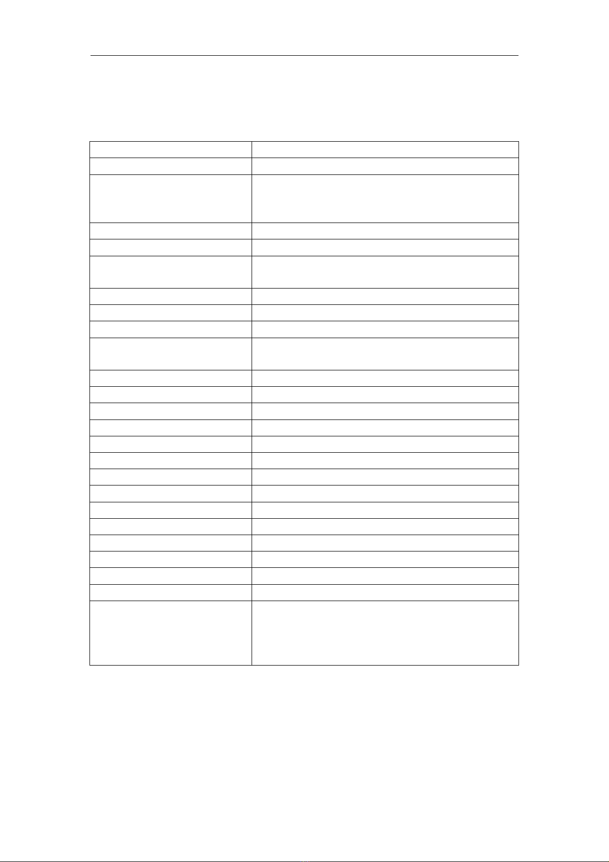
4.1 RF Components................................................................................................... 7
4.2 RX Trouble........................................................................................................... 8
4.2.1 Check ANT Feedback Points..................................................................... 8
4.2.2 Check Regulator Circuit............................................................................. 8
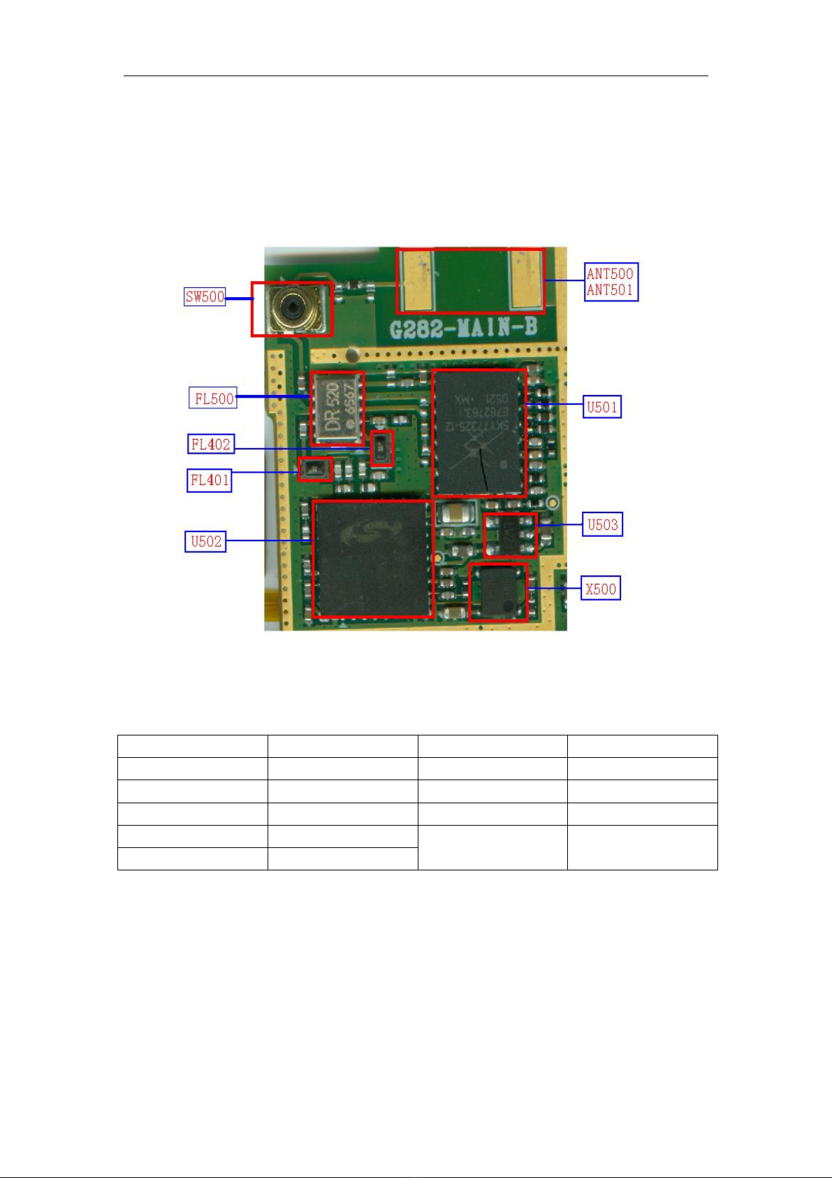
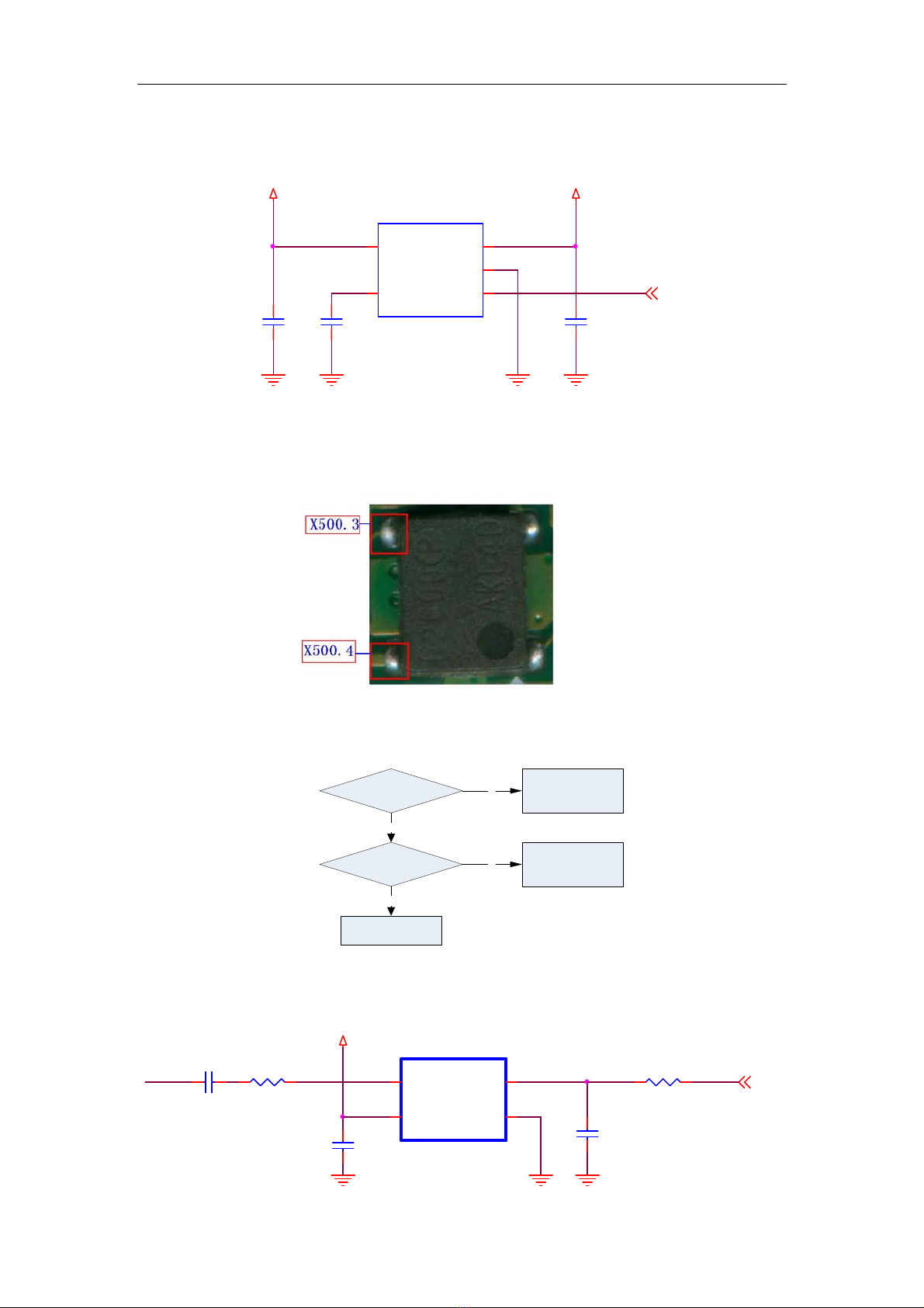
4.2.3 Check VCTCXO Circuit.............................................................................. 9
4.2.4 Check Antenna Switch & Mobile Switch....................................................10
4.2.5 Check SAW Filter......................................................................................11
4.2.6 Checking Receive IQ................................................................................12
4.3 TX Trouble ..........................................................................................................13
4.3.1 Check LDO Circuit....................................................................................13
4.3.2 Check VCTCXO Circuit.............................................................................13
4.3.3 Check Transmit IQ....................................................................................13
4.3.4 Check PAM Control Signal........................................................................14
4.3.5 Check Antenna Switch and Mobile Switch................................................15
4.4 Power On Trouble...............................................................................................15
4.5 Charging Trouble ................................................................................................17
4.6 LCD Trouble....................................................................................................... 19
4.6.1 LCD Blue Screen..................................................................................... 19
4.6.2 LCD Blank Screen or Abnormal Screen................................................... 19
4.7 Camera Trouble..................................................................................................20
4.8 Color LED Trouble ..............................................................................................21
4.9 KEYPAD Blacklight LEDS Trouble......................................................................22
4.10 SIM Trouble.......................................................................................................23
4.11 Ear Jack Trouble ...............................................................................................24
4.12 Speaker/Receiver Trouble.................................................................................26
5. DOWNLOAD AND CALIBRATION .............................................................28
6. CIRCUIT DIAGRAM & PCB LAYOUT…………………………………………29
7. EXPLODED VIEW & REPLACEMENT PART LIST………………………….36

1. INTRODUCTION
1. INTRODUCTION
1.1 Purpose
This manual provides the information necessary to repair, calibration, description and
download the features of LG-C3600.
1.2 Regulatory Information
A. Security
Toll fraud, the unauthorized use of telecommunications system by an unauthorized part
(for example, persons other than your company’s employees, agents, subcontractors, or
person working on your company’s behalf) can result in substantial additional charges for
your telecommunications services. System users are responsible for the security of own
system.There may be risks of toll fraud associated with your telecommunications system.
System users are responsible for programming and configuring the equipment to prevent
unauthorized use. The manufacturer does not warrant that this product is immune from
the above case but will prevent unauthorized use of common – carrier telecommunication
service of facilities accessed through or connected to it. The manufacturer will not be
responsible for any charges that are resulted from such unauthorized use.
B. Changes in Service
A local telephone company may make changes in its communications facilities or
procedure. If these changes could reasonably be expected to affect the use of this phone
or compatibility with the network, the telephone company is required to give advanced
written notice to the user, allowing the user to take appropriate steps to maintain
telephone service.
C. Maintenance Limitations
Maintenance limitations on this model must be performed only by the manufacturer or its
authorized agent. Therefore, note that unauthorized alternations or repair may affect the
regulatory status of the system and may void any remaining warranty.
D. Notice of Radiated Emissions
This model complies with rules regarding radiation and radio frequency emission as
defined by local regulatory agencies. In accordance with these agencies, you may be
required to provide information such as the following to the end user.
E. Interference and Attenuation
Phone may interfere with sensitive laboratory equipment, medical equipment, etc.
Interference from unsuppressed engines or electric motors may cause problems.
F. Electrostatic Sensitive Devices
1

1. INTRODUCTION
ATTENTION
Boards, which contain Electrostatic Sensitive Device (ESD), are indicated by the sign.
Following information is ESD handling:
• Service personnel should ground themselves by using a wrist strap when exchange
system boards.
• When repairs are made to a system board, they should spread the floor with anti-static
mat which is also grounded.
• Use a suitable, grounded soldering iron.
• Keep sensitive parts in these protective packages until these are used.
• When returning system boards or parts like EEPROM to the factory, use the protective
package as described.
2

2. SYSTEM SPECIFICATION
Item Target Specification
Form Factor Folder Type
Standard Battery (1000mAh , Li-ion)
Size:34(W)×50(H)×5.5(T) mm
Weight:25g
Size 88 X 44 X 23mm
Weight 88.35 Gram(with standard battery)
Standby Current Below 4.5mA under the least current consumption
(e.g. Paging Period = 9)
Talk Time Up to 3 hrs (GSM Tx Lev:5)
Standby Time Up to 200 hrs : Paging Period 9, RSSI 85dBm
Antenna Internal
LCD Main LCD:CSTN 128×160 Pixels 65K Color
Sub LCD: CSTN 96×64 Pixels 65K Color
Back Light Blue LED
PC Sync Yes
Indicator LED None
Vibrator Yes (Cylinder Type)
Buzzer Yes
C-MIC Yes
Receiver Yes
Earphone Jack Yes (Stereo)
SIM Socket Yes (SIM Block Type)
Volume Key Yes
Voice Key Yes
MP3/AAC Yes
MIDI 64 MIDI
I/O Connector 24Pin
Basic Accessory Travel Adaptor
Standard Battery (1000mAh , Li-ion)
Ear-mic
Data Cable
3

3. TECHNICAL BRIEF
3. LG-C3600 TECHNICAL BRIEF
3.1 LG-C3600 Block Diagram
Figure 3-1 LG-C3600 top level block diagram
The Figure 3-1 shows the top level block diagram of LG-C3600, it contains RF and BB part.
The following list is the detailed:
1. AD6527B : ADI digital baseband chipset
2. AD6537B : ADI analog baseband and power supply chipset
3. SI4205 : RF transmitter chipset
4. NEC9993 : NEC MP3 and Midi chipset
5. RD38F4455LLZDQ0 : 256Mb + 256Mb intel Flash memory chipset
6. CL761S : Camera module
7. Others:
A. 24 main key, 3 MP3 play key and 2 side key.
B. 128 x 160 65K CSTN –LCD module
C. Vibrator
D. Mic
E. Speaker and receiver
F. Ear-jack
G. Sim socket
H. Battery connector
4

3. TECHNICAL BRIEF
3.2 RF Part
The RF parts consist of a transmitter part, a receiver part, a frequency synthesizer part, a
voltage supply part, and a VCTCXO part. The Aero transceiver is one chip solution which
supports dual and triple-band GSM/GPRS wireless communications. This device
integrated a receiver based on a low IF(100KHz) architecture and a transmitter based on
a modulation loop architecture which contains a complete dual band transceiver with built
in VCOs. The transceiver employed a 3 wire serial interface to allow an external system
controller to write the control registers for dividers, receive path gain, power down setting,
and other controls.
Figure 3-2 Receiver Block Diagram
Figure 3-3 Frequency Synthesizer Block Diagram
Figure3-4 Transmitter Block Diagram
5

3. TECHNICAL BRIEF
3.3 BaseBand Transmit Section
i. The AD6537B transmit section is designed to support GMSK for both single slot and
multislot applications.
ii. The AD6537B transmit section consists of a digital GMSK modulator, a matched pair of
10-bit DACs and a matched pair of reconstruction filter.
Figure 3-5 AD6537B BASEBAND TRANSMIT SECTION
3.4 BaseBand Receive Section
i. This section consists of two identical ADC channels that process baseband in-phase(I)
and quadrature(Q) signals.
ii. Each channel consists a coarse switched capacitor Anti-alias filter, followed by a low
pass digital filter.
Figure 3-6 AD6537B BASEBAND RECEIVER SECTION
6

4. TROUBLE SHOOTING
4. LG-C3600 TROUBLE SHOOTING
4.1 RF Components
Figure 4-1 RF Components
Reference Description Reference Description
SW500 Mobile S/W U501 PAM
FL401 EGSM SAW Filter FL500 ANT S/W
FL402 DCS SAW Filter U503 LDO
U502 RF Main Chipset
X500 XCTCXO
ANT500
ANT501 ANT Feedback
Point
Table 4-1
7

4. TROUBLE SHOOTING
4.2 RX Trouble
START
HP8922:Test M ode
62CH ,7 Level Setting(TCH0
62CH ,-6 0 d B m S ettin g (BCCH)
1 C heck A N T
Feedback Pints
2 Check Regulator
Circuit
3 CheckVCTCX O
Circuit
4 C heck A N T SW
& M o bile S W 5 Check SA W
F ilter C ircu it
6 C heck R eceiving
IQ
Redow nload SW ,Cal
4.2.1 Check ANT Feedback Points
See Figure 4-1. Check ANT500 and ANT501 Check Wether theANT Good Contacting
4.2.2 Check Regulator Circuit
Figure 4-2 Regulator Circuit
Regulator Circuit OK see
Next Page
Check VCTCXO
RF 2.8V OK? PIN6 HIGH ?
Replace the
U503
Change the
Board
YES
Check PIN5 Check PIN 1
NO NO
YES
8

4. TROUBLE SHOOTING
U503
MIC5255-2.85BM5
5
4 3
1
2
OUT
BYP EN
IN
GND
RF 2.85V
RF_LDO
C535
22n
VBAT
C529
4.7n
(1608)
C536
4.7u
CLKON
AFC
4.2.3 Check VCTCXO Circuit
Figure 4-3 VCTCXO Circuit
13Mhz Right?
2.75v Right?
Check U101
VCTCXO Circuit
no problem, check
below, or software
Replace X501
Y
Y
N
N
Chec Pin3
Figure 4-3
Check Pin 4
Figure 4-3
C539
2.2u
C528
100p
X500
26MHz
4
3
2
1
VCC
OUT
GND
VCONT
2V75_VVCXO
R515 10K
C540
0.1u
R510
100
9

4. TROUBLE SHOOTING
4.2.4 Check Antenna Switch & Mobile Switch
Figure 4-4 Antenna Switch & Mobile Switch
Tx Test Only
(GSM:PL=7,DCS
:PL=2)
Check C531,C537,
Whether phone in Rx
state , Figure 4-4
VC1:L
VC2:L Pin5:-29.5dBm
Pin3:-26.5dBm
Check FL501 pin
10(For GSM)&Pin1(For
DCS) Power Level
Start Shorten?
Check SW500 RF cable
Connection
Change Main
Board
Check Pin 4,3,5
PAM control Signal Replace SW500 Replace
SW500
Y
NNN N
YY End
Y
Table 4-2
10

4. TROUBLE SHOOTING
4.2.5 Check SAW Filter
Figure 4-5
C518 1p
C522 1p
C513 1p
C510
27p
FL502
EFCH1842TCA7
1
23
54
IN G
1O
1
G
2O
2
C521 1p
L503 6.8nH
FL501
EFCH942MTCA7
1
23
54
IN G
1O
1
G
2O
2
L501 27nH
FL401.1:
~-61dBm
FL401.3:~-64dBm
FL402.3:~-64dBm
Change C510 (For
GSM)
Check the
soldering Is
Ok?
C510(for GSM)
The SAW
soldering Is
Ok?
Change
For GSM:L501,C513
For DCS:L503,C521
Change
FL401(GSM)
FL402(DCS)
Check the soldering
Is Ok?
For GSM:L501,C513
For DCS:L503,C52
SAW filer is OK, Refer
next page for IQ
signal checking
Check the SAW filter
Output
For GSM:FL401.3
For DCS:FL402.3
When do these two
test, standalone mode
should be applied
Yes
Yes
No
No
No
Yes
Check the SAW filter
Iutput
For GSM:FL401.3
For DCS:FL402.3
11

4. TROUBLE SHOOTING
4.2.6 Checking Receive IQ
Figure 4-6
check C519,C526
check if there is any
major difference
Refer to Figure4-6
Sililar?
Redownload software
Recalibrate
Replace U102
No
Yes
Figure 4-7
12

4. TROUBLE SHOOTING
4.3 TX Trouble
Start
HP8922:Test Mode
Set 62CH,7 level(TCH0
Set 62CH,-60dBm level(BCCH)
1、check LDO
circuit
2、check VCTCXO
circuit
3、check antenna
and mobile
communication S/W
5、check RAM
control signal
Download S/W and calibration
again.
3、check antenna
and mobile
communication S/W
4.3.1 Check LDO Circuit
Detail on 4.2.1
4.3.2 Check VCTCXO Circuit
Detail on 4.2.2
4.3.3 Check Transmit IQ
Detail on 4.2.6
13

4. TROUBLE SHOOTING
4.3.4 Check PAM Control Signal
Figure 4-8
U502
SKY77325
4
2
6
5
8
3
1
2
0
1
9
2
2
2
32
11
81
61
41
31
11
097
15
12
17
BS
PAC_ENABLE
GSM_IN
DCS_PCS_IN
V
C
C
1
B
V
C
C
1
A
N
C
V
B
A
T
T
V
S
E
N
S
E
V
A
P
C
P
G
N
D
G
N
D
9
G
N
D
8
G
N
D
7
G
N
D
6
G
N
D
5
G
N
D
4
G
N
D
3
G
N
D
2
G
N
D
1
RSVD
GSM_OUT
DCS_OCS_OUT
GPIO_17
C501
27p
C581
12p
C504
0.01u
PA_EN
PA_BAND
TX_RAMP
C503
0.01u
C506
0.01u
C502
33p
GPIO_16
R501 100
C507
22u
VBAT
C505
18p
C520
39P
R509
1k
C509
27p
R502 100
Almost the
same?
Transmit IQ signal OK,
Check RF transmit level
reference on next page.
Download S/W
again
Check TX-RAMP and
PA-EN
Check the
difference
*Reference Graph
4-8 Yes
No
14

4. TROUBLE SHOOTING
Figure 4-9
4.3.5 Check Antenna Switch and Mobile Switch
Please refer to 4.2.4
4.4 Power On Trouble
Figure 4-10
15

4. TROUBLE SHOOTING
START
Battery Voltage
>3.35 V
Charge or Change
Battery
Check the Contact of
PowerKey or Dome
Change Dome
Check the Following Pins
of U102
C113
=1.8
V?
C121
=
2
.
75 V ?
C114 =2
.8
V
?
C115 =1
.
8V
?
Replace U102
Logic Level of Pin3 of
D101 = HIGH?
Redownload Software
Phone will Power On
Yes
Yes
Yes
Yes
No
No
No
No
16

4. TROUBLE SHOOTING
4.5 Charging Trouble
Figure 4-11
R126 100
D102
CUS02
C
1
4
3
1
u
C152 1u
VBAT
+
C126
10U
R122 1.2M 1%
R108
330
Q100
TPCF8102
1
2
3
4
8
7
6
5
D1
D2
D3
G
D6
D5
D4
S
R
1
0
6
0
.
2
C151 0.01u
U205
IBIAS
CRST
VMEMSEL
VBACKSEL
C
_G16_VPLL_TE
CHGDACREF
CHGOSC
VBATSENSE
VCHG
ISENSE
GATEDRIVE
VCHARGE
17

4. TROUBLE SHOOTING
I/O Connector
(CN301) is well-
soldered?
START
Voltage atAnode
of D102 = 5.2 V ?
Q100, D102, R106
are well-soldered?
Voltage
across R106 is about
10~100mV?
Battery is OK? The battery may have
problems. Change the battery.
Charging is
operating properly .
Replace the Q100, D102
Resolder the
Q100, D102, R106
The TA is out of order.
Change the TA .
Re-solder the CN301 (Pin
4,5:VCHARGE, Pin 12,19:GND)
Yes
Yes
Yes
Yes
Yes
Yes
No
No
No
No
No
18

4. TROUBLE SHOOTING
4.6 LCD Trouble
4.6.1 LCD Blue Screen
Figure 4-12
Can the
main board
poweron? LCD is OK.
Go to power
on trouble Reconnect
the connectors Replace
FL600, FL602 Change LCD
Yes Yes Yes
No No
Check the
connection between
FPCB and PCB , FPCB
and LCD
Check the
signal ofFL600,
FL602
Is LCD
moduleOK?
Yes
No No
4.6.2 LCD Blank Screen or Abnormal Screen
Figure 4-13
Can the
main board
poweron? LCD is OK.
Go to power
on trouble Reconnect
the connectors Replace U402 Change LCD
Yes Yes Yes
No No
Check the
connection between
FPCB and PCB , FPCB
and LCD
Check the
output signal of
FB403
Is LCD
moduleOK?
Yes
No No
19
Other manuals for C3600
1
Table of contents
Other LG Cell Phone manuals