LG L240 User manual

- 3 -
1. Introduction ..................................... 5
1.1 Purpose................................................... 5
1.2 Regulatory Information............................ 5
2. Performance .................................... 7
2.1 HW Feature............................................. 7
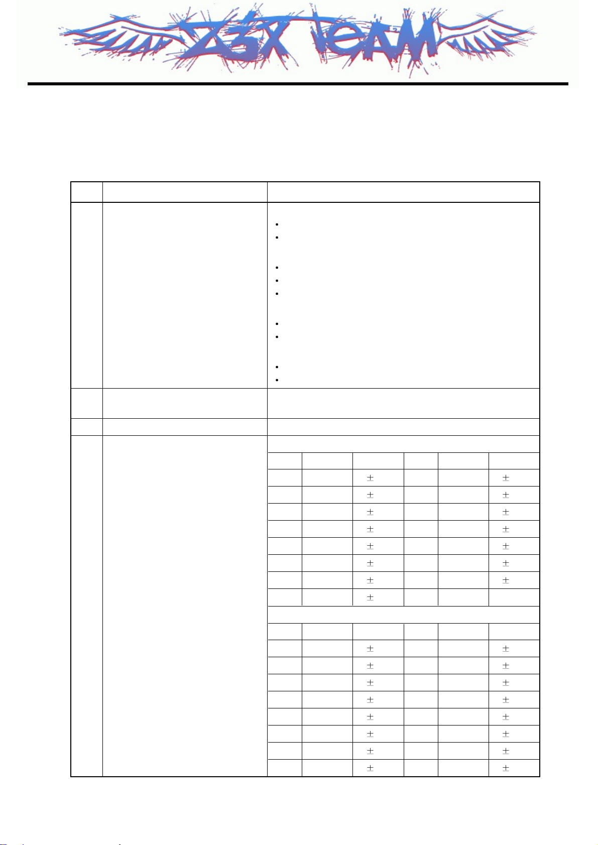
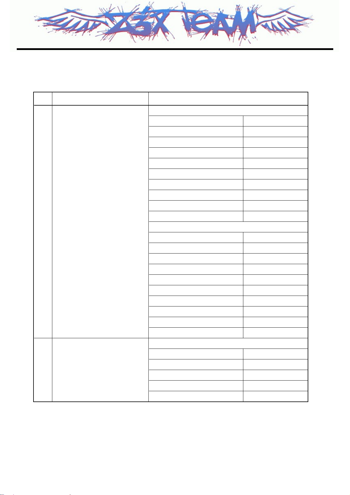
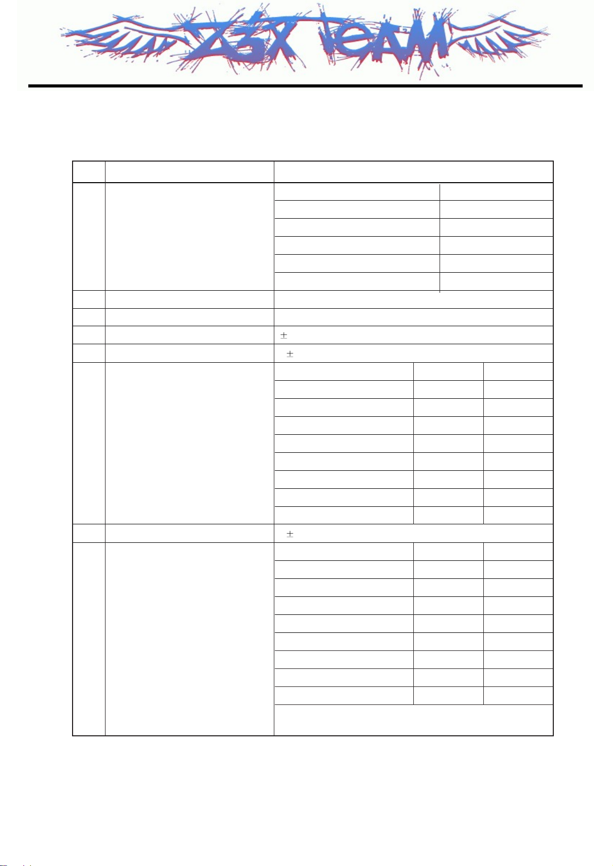
2.2 Technical Specification ........................... 9
3. Circuit Description........................ 14
3.1 General Description .............................. 14
3.2 RF Part.................................................. 14
3.3 Digital Baseband................................... 20
3.4 Analog Baseband.................................. 26
3.5 Bluetooth Interface................................ 34
4. TROUBLE SHOOTING .................. 37
4.1 RF Part Technical Brief......................... 37
4.2 RF Part Trouble shooting...................... 43
4.3 Bluetooth Trouble Shooting .................. 51
4.4 Baseband Part Troubleshooting ........... 55
4.5 LCD Display Trouble............................. 61
4.6 Camera Trouble Shooting..................... 65
4.7 MOD Key Trouble Shooting .................. 67
4.8 SIM Detect Trouble Shooting................ 71
4.9 Folder On/Off and Trouble Shooting..... 73
4.10 Speaker Trouble Shooting .................. 75
4.11 Receiver Trouble Shooting ................. 78
4.12 MIC Trouble Shooting ......................... 79
4.13 Transflash Trouble Shooting............... 81
4.14 Keypad Backlight LED Trouble
Shooting.............................................. 83
4.15 Vibrator Trouble Shooting................... 85
4.16 Ear-Mic Jack Detection
Trouble Shooting..................................86
4.17 Ear-Mic Hook Detection
Trouble Shooting..................................87
4.18 Ear-Mic Headset MIC
Trouble Shooting..................................88
4.19 Ear-Mic Headset HSOR/HSOL
Trouble Shooting..................................89
5. Downloading Software ................. 91
5.1 The purpose of downloading software.. 91
5.2 The Environment of Downloading
Software................................................ 91
5.3 Download Procedure .............................93
6. BLOCK DIAGRAM ......................... 97
7. CIRCUIT DIAGRAM ....................... 99
8. PCB LAYOUT............................... 106
9. RF Calibration................................... 109
9.1 RF Calibration Equipment Setup....... 109
9.2 RF Calibration Procedure.................. 109
12. EXPLODED VIEW &
REPLACEMENT PART LIST ..... 113
12.1 EXPLODED VIEW ............................ 113
12.2 Replacement Parts
<Mechanic component>.................... 115
<Main component> ........................... 118
12.3 Accessory ......................................... 132
Table of Contents
Z3X-BOX.COM

1. Introduction
- 5 -
1.1. Purpose
This manual provides the information necessary to repair, calibration, description and download the
features of this model.
1.2. Regulatory Information
A. Security
Toll fraud, the unauthorized use of telecommunications system by an unauthorized part (for example,
persons other than your company’s employees, agents, subcontractors, or person working on your
company’s behalf) can result in substantial additional charges for your telecommunications services.
System users are responsible for the security of own system. There are may be risks of toll fraud
associated with your telecommunications system. System users are responsible for programming and
configuring the equipment to prevent unauthorized use. The manufacturer does not warrant that this
product is immune from the above case but will prevent unauthorized use of common-carrier
telecommunication service of facilities accessed through or connected to it.
The manufacturer will not be responsible for any charges that result from such unauthorized use.
B. Incidence of Harm
If a telephone company determines that the equipment provided to customer is faulty and possibly
causing harm or interruption in service to the telephone network, it should disconnect telephone
service until repair can be done. A telephone company may temporarily disconnect service as long as
repair is not done.
C. Changes in Service
A local telephone company may make changes in its communications facilities or procedure. If these
changes could reasonably be expected to affect the use of the this phone or compatibility with the
network, the telephone company is required to give advanced written notice to the user, allowing the
user to take appropriate steps to maintain telephone service.
D. Maintenance Limitations
Maintenance limitations on this model must be performed only by the manufacturer or its authorized
agent. The user may not make any changes and/or repairs expect as specifically noted in this manual.
Therefore, note that unauthorized alternations or repair may affect the regulatory status of the system
and may void any remaining warranty.
1. Introduction
Z3X-BOX.COM

1. Introduction
- 6 -
E. Notice of Radiated Emissions
This model complies with rules regarding radiation and radio frequency emission as defined by local
regulatory agencies. In accordance with these agencies, you may be required to provide information
such as the following to the end user.
F. Pictures
The pictures in this manual are for illustrative purposes only; your actual hardware may look slightly
different.
G. Interference and Attenuation
Phone may interfere with sensitive laboratory equipment, medical equipment, etc.Interference from
unsuppressed engines or electric motors may cause problems.
H. Electrostatic Sensitive Devices
ATTENTION
Boards, which contain Electrostatic Sensitive Device (ESD), are indicated by the sign.
Following information is ESD handling:
•Service personnel should ground themselves by using a wrist strap when exchange system boards.
•When repairs are made to a system board, they should spread the floor with anti-static mat which is
also grounded.
•Use a suitable, grounded soldering iron.
•Keep sensitive parts in these protective packages until these are used.
•When returning system boards or parts like EEPROM to the factory, use the protective package as
described.
Z3X-BOX.COM

2. PERFORMANCE
- 7 -
2.1 HW Feature
2. Performance
Item Feature Comment
Form Factor Clamshell with External Display
1) Capacity
Battery Standard : Li-Ion, 900mAh (LGC)
2) Packing Type : Soft Pack
Size Standard :
89.0 X 47.0 X 22 mm
Weight 90g With Battery
Volume 75cc
PCB Staggered 8 Layers , 0.8t
Stand by time 250 hrs @Paging Period 9
Charging time 3 hrs @ Power Off / 900mAh
Talk time Min : 2.5 hrs @ Power Level 5 @ GSM850 / 900mAh
GSM 850 : -105 dBm
RX sensitivity EGSM : -105 dBm
DCS 1800 : -105 dBm
PCS 1900 : -105 dBm
GSM/ GSM 850 : 33 dBm Class4 (GSM850)
GPRS EGSM : 33 dBm Class4 (EGSM)
DCS 1800 : 30 dBm Class1 (PCS)
TX output power PCS 1900 : 30 dBm Class1 (DCS)
EDGE GSM 850 : 27 dBm E2 (GSM850)
EGSM : 27 dBm E2 (EGSM)
DCS 1800 : 26 dBm E2 (PCS)
PCS 1900 : 26 dBm E2 (DCS)
GPRS compatibility GPRS Class 10
EDGE compatibility EDGE Class 10
SIM card type Plug-In SIM
3V /1.8V
Main LCD
256K Color TFT (128 X160)
Display Backlight : White LED
Sub LCD
65K CSTN (96X64)
Z3X-BOX.COM

2. PERFORMANCE
- 8 -
Item Feature Comment
Status Indicator Indicator LED in MOD KEY
Alphanumeric Key : 12 Function Key:
Function Key : 12 4 Key Navigation, OK,
Mod Key : 3 F1, F2, Camera, CLR,
Keypad Side Key : 3 SND, END/PWR, MP3
Total No of Keys :30 Player
Mod Key :
RW, Play/Pause, FW
ANT Main : External Fixed Type
Blue tooth : Intenna
System connector 24 Pin
Ear Phone Jack 4 Pole (2.5mm), Stereo
PC synchronization Yes
Memory Flash : 512Mbit
SDRAM : 256Mbit
Speech coding FR, EFR, HR,AMR
Data & Fax Built in Data & Fax support
Vibrator Built in Vibrator
Blue Tooth V2.0(Except EDR support)
A2DP, HFP, BPP support
MIDI (for Buzzer Function) SW Decoded 64Poly
Music Player MP3/ AAC/AAC+ With Graphic EQ
Camcorder MPEG4+AMR
Voice Recording Yes
Speaker Phone mode Yes
Support
Travel Adapter Yes
CDROM Yes
Stereo Headset Yes Optional
Data Cable Yes Optional
T-Flash (External Memory)
Yes Optional
Z3X-BOX.COM

2. PERFORMANCE
- 9 -
2.2 Technical Specification
Item Description Specification
GSM850
TX: 824 + n ¢• 0.2 MHz (n=1 ~ 124)
RX: TX + 45 MHz
GSM900
TX: 890 + n ¢• 0.2 MHz (n=1 ~ 124)
890 + (n-1024) ¢• 0.2 MHz (n=975 ~ 1023)
RX: TX + 45 MHz
1Frequency Band DCS1800
TX: 1710 + ( n-511 ) ¢• 0.2 MHz (n = 512 ~ 885)
RX: TX + 95 MHz
PCS1900
TX: 1850 + ( n-511 ) ¢• 0.2 MHz
RX: 1930 + ( n-511 ) ¢• 0.2 MHz (n = 512 ~ 810)
2Phase Error RMS < 5 degrees
Peak < 20 degrees
3Frequency Error < 0.1ppm
GSM850/GSM900
Level Power Toler. Level Power Toler.
533 dBm 2dB 13 17 dBm 3dB
631 dBm 3dB 14 15 dBm 3dB
729 dBm 3dB 15 13 dBm 3dB
827 dBm 3dB 16 11 dBm 5dB
925 dBm 3dB 17 9 dBm 5dB
10 23 dBm 3dB 18 7 dBm 5dB
11 21 dBm 3dB 19 5 dBm 5dB
4Power Level 12 19 dBm 3dB
DCS1800/PCS1900
Level Power Toler. Level Power Toler.
030 dBm 2dB 8 14 dBm 3dB
128 dBm 3dB 9 12 dBm 4dB
226 dBm 3dB 10 10 dBm 4dB
324 dBm 3dB 11 8 dBm 4dB
422 dBm 3dB 12 6 dBm 4dB
520 dBm 3dB 13 4 dBm 4dB
618 dBm 3dB 14 2 dBm 5dB
716 dBm 3dB 15 0 dBm 5dB
Z3X-BOX.COM

2. PERFORMANCE
- 10 -
Item Description Specification
GSM850/GSM900
Offset from Carrier (kHz). Max. dBc
100 0.5
200 -30
250 -33
400 -60
600~ <1,200 -60
1,200~ <1,800 -60
1,800~ <3,000 -63
3,000~ <6,000 -65
5Output RF Spectrum 6,000 -71
(due to modulation) DCS1800/PCS1900
Offset from Carrier (kHz). Max. dBc
100 0.5
200 -30
250 -33
400 -60
600~ <1,200 -60
1,200~ <1,800 -60
1,800~ <3,000 -65
3,000~ <6,000 -65
6,000 -73
GSM850/GSM900
Offset from Carrier (kHz) Max. (dBm)
Output RF Spectrum 400 -19
6(due to switching transient) 600 -21
1,200 -21
1,800 -24
Z3X-BOX.COM

2. PERFORMANCE
- 11 -
Item Description Specification
DCS1800/PCS1900
Offset from Carrier (kHz). Max. (dBm)
Output RF Spectrum 400 -22
6(due to switching transient) 600 -24
1,200 -24
1,800 -27
7Spurious Emissions Conduction, Emission Status
8Bit Error Ratio BER (Class II) < 2.439% @-102dBm
9Rx Level Report accuracy 3 dB
10 SLR 8 3 dB
Frequency (Hz) Max.(dB) Min.(dB)
100 -12 -
200 0 -
300 0 -12
11 Sending Response 1,000 0 -6
2,000 4 -6
3,000 4 -6
3,400 4 -9
4,000 0 -
12 RLR 2 3 dB
Frequency (Hz) Max.(dB) Min.(dB)
100 -12 -
200 0 -
300 2 -7
500 *-5
13 Receiving Response 1,000 0 -5
3,000 2 -5
3,400 2 -10
4,000 2
*Mean that Adopt a straight line in between 300 Hz and
1,000 Hz to be Max. level in the range.
Z3X-BOX.COM

2. PERFORMANCE
- 12 -
Item Description Specification
14 STMR 13 5 dB
15 Stability Margin > 6 dB
dB to ARL (dB) Level Ratio (dB)
-35 17.5
-30 22.5
-20 30.7
16 Distortion -10 33.3
033.7
731.7
10 25.5
17 Side Tone Distortion Three stage distortion < 10%
18 <Change> System frequency 2.5ppm
(13 MHz) tolerance
19 <Change>32.768KHz tolerance 30ppm
GSM850/Lvl 7 (Battery Capacity 900mA) : 180 min
20 Talk Time GSM850/Lvl 12 (Battery Capacity 900mA) : 240 min
Under conditions, at least 200 hours:
1. Brand new and full 900mAh battery
2. Full charge, no receive/send and keep GSM in idle mode.
21 Standby Time 3. Broadcast set off.
4. Signal strength display set at 3 level above.
5. Backlight of phone set off.
At least 55 dB under below conditions:
22 Ringer Volume 1. Ringer set as ringer.
2. Test distance set as 100 cm
23 Charge Voltage Fast Charge : < 550 mA
Slow Charge: < 100 mA
Antenna Bar Number Power
5-85 dBm ~
4-90 dBm ~ -86 dBm
24 Antenna Display 3 -95 dBm ~ -91 dBm
2-100 dBm ~ -96 dBm
1-105 dBm ~ -101 dBm
0~-105 dBm
Z3X-BOX.COM

2. PERFORMANCE
- 13 -
Item Description Specification
Antenna Bar Number Power
03.62V 0.03V
25 Battery Indicator 1 3.70V 0.03V
23.78V 0.03V
33.91V 0.03V
43.92V 0.03V↑
26 Low Voltage Warning 3.62V↓0.03V (Call)
3.50V↓0.03V (Standby)
27 Forced shut down Voltage 3.35 0.03 V
1 Li-ion Battery
28 Battery Type Standard Voltage = 3.7 V
Battery full charge voltage = 4.2 V
Capacity: 900mAh
Switching-mode charger
27 Travel Charger Input: 100 ~ 240 V, 50/60Hz
Out put: 4.8V, 900mA
Z3X-BOX.COM

3. Circuit Description
- 14 -
3.1 General Description
The RF part consists of a transmitter, a receiver, a synthesizer, a voltage supply and a VC-TCXO part.
The main RF Chipset MMM6000 is a transceiver for the GSM, GPRS, and EDGE standards, providing
antenna-todigital- bits functionality. The transceiver functions over the GSM850, EGSM900, DCS1800,
and PCS1900 transmit and receive frequency bands. The MMM6000 transceiver includes a VLIF/DCR
receive architecture and a polar modulation transmit architecture with direct modulation of the VCO by
a fractional-N synthesizer. Both the RX and TX VCOs are fully integrated. The polar architecture
allows for a filter-free transmit lineup. An on-chip transmit/receiver sequencer generates appropriate
timing events for the transmitter calibration and the EDGE / GMSK transmit/receive burst, therefore,
limiting the RF hardware dependency of the L1 engine software to an absolute minimum. The DigRF
standard defines the digital interface between the MMM6000 and the base band processor IC,
allowing maximum industry compatibility.
3.2 RF Part
3.2.1 Receiver Part
The Receiver part in MMM6000 contains all active circuits completely, full receiver chain with the
exception of discrete front-end RF SAW filters. The filtered and amplified signal is down converted in
the RF-mixer to the ba se-band output. The receive path is supported by internal channel filtering.
3. Circuit Description
<Fig.1> Receiver Part Block Diagram
Z3X-BOX.COM

3. Circuit Description
- 15 -
3.2.1.1 Front End Part
The RF front end consists of Antenna Switch, quad saw filters and LNAs integrated in transceiver .
Antenna switch is integrated in MMM6027 (Raptor) and quad saw filters are integrated in saw filter
bank. The Received RF signals (GSM850,900, PCS, DCS) are fed into the antenna and Mobile
switch. An antenna matching circuit is between the antenna and the mobile switch. The Antenna
Switch in Raptor is used to control the Rx and Tx paths. And, the input signals TX_ANT_SW_EN,
LB_HB and US_EURO of Raptor are connected to transceiver controller to switch either Tx or Rx
path on. Antenna Switch supports for quad band.
The FEM control logics given below Table 1
The receiver part uses a very low-IF (VLIF) conversion architecture that allows for the on-chip
integration of the DC offset compensation system, eliminating DC offset from the demodulated signal.
The MMM6000 integrates quad differential input LNAs that are matched to the 200 ohm with
balanced-output SAW filter bank through LC matching networks in SAW filter bank.
3.2.1.2 Demodulator and base-band processing
The RX architecture is digital VLIF/DCR. There are four separate LNAs providing functionality for
GSM850, EGSM900, DCS1800 and PCS1900 frequency bands. The LNAs are differential and
provide 30 dB of dynamic range as digital steps, eliminating the need for RX AGC gain. The
quadrature down mixer converts the RF signal to base band. Passive differential and common mode
filtering at the mixer output limits out of band signals in the active stages of the base band section
and results in an IP2 of 55 dBm (including processor gain). The I and Q analog base band signals are
passed through low pass anti-aliasing filters and dc offset correction circuits before being processed
by the analog-to-digital converters.
Switch Mode TX_ANT_SW_EN LB_HB US_EURO
GSM850 Rx Low Low Low
EGSM Rx Low Low High
DCS Rx Low High High
PCS Rx Low High Low
GSM850 Tx High Low Low
EGSM Tx High Low High
DCS Tx High High High
PCS Tx High High Low
<Table 1> Control Logics
Z3X-BOX.COM

3. Circuit Description
- 16 -
3.2.2 Synthesizer Part
Both the RX and TX VCO run at 3296 to 3820 MHz and have integrated resonators with 32 states of
digital course tuning. The frequency synthesizer is a 24-bit, 3rd order fractional N synthesizer with
digital AFC and a lock time of less than 80µs. A 26 MHz TCXO provides a stable frequency
reference. The VCO output signal runs through a divide-by-two for operation in the DCS/PCS bands
and a divide-by-four for operation in the 850GSM and EGSM bands. Operation at 2 or 4 times the LO
frequency provides good immunity to remodulation. VCO feedback to the “divide-by-N” is through a
fixed divide-by-3. The output of the divide-by-N is compared to a 26 MHz reference in the phase
comparator and error output is passed through the loop filter before being applied to the VCO.
The corrected clock module is a 22-bit digital phase-locked loop used to provide an accurate 26 MHz
reference, synchronized to the GSM system, when the system is operated from an uncorrected
TCXO. The 26 MHz reference TCXO provides a stable frequency reference for the major functions in
the radio system. The TCXO output can also be routed to two auxiliary reference pins to provide a
reference clock for RF accessories such as Bluetooth, GPS, and WLAN.
3.2.3 Transmitter Part
The Transmitter part contains polar modulator part of RF main chipset [MMM6000] and Power
Amplifier Module [MMM6027]
3.2.3.1 Polar Modulator Part
The TX architecture is a polar modulator with direct digital modulation of the VCO. The module can
transmit in GMSK (phase modulation) or 8PSK (phase and amplitude modulation) mode. In GMSK
mode, the dual port TX VCO is phase modulated by the dual port synthesizer and the signal is fed to
the PA input at a fixed level. In 8PSK mode, the additional amplitude modulation is performed via a
commuting switch mixer. The mixer core drives a resistive digital step attenuator, which provides 0 to
45 dB of dynamic range in 3 dB steps, allowing the required full dynamic range to cover all EDGE
power steps with only 20 dB of dynamic range from the modulator. Two DACs provide signals to the
modulator. One DAC is dedicated to the amplitude component of the 8PSK wave form and the other
to driving the VCO high port input.
Z3X-BOX.COM

3. Circuit Description
- 17 -
3.2.3.2 Power Amplifier Part
The Power Amplifier Module [MMM6027] is a quad-band Class 10 GSM, GPRS, EDGE Power
Amplifier Front End Module (FEM) functioning over the GSM850, EGSM900, DCS1800, and
PCS1900 transmit and receive frequency bands.
To simplify radio front-end design, power amplification, power coupling, power detection, low-pass
filtering output power control, and antenna switching functions are integrated into the Power Amplifier
FEM.
The Power Amplifier Module [MMM6027] is specified to operate with both GMSK and 8PSK
modulation schemes and is intended to be used in combination with the transceiver [MMM6000]. Two
modes of power control are supported with the MMM6027: bias control for GMSK modulation and
input power control for 8PSK modulation.
SAW
Filter
Module
PA Bias Control
PowerDetection
PowerControl
Switch Con trol
Couplers
+
Harmonic
Filters
Anten na
Switch
˜2
90
°
˜4
90
°
LPF
˜2
˜2
LPF
AM PLITUDE M ODULATION
LPF
PHASE MODULATION
HI
PORT
TX VCO
LO-PORT
DigitalRadio
Receiver
RF
Synthesizer
Transmit
Modulator
PA Control
(PAC)
RX VCO
MM M6000
Quad-Band
GSM/GPRS/EDGE
TRANSCEIVER
DigRF
Power Amplification
PowerDetection& Conrol
Antenna Switching
<Fig.2> MMM6000 & MMM6027 Block Diagram
<Fig.3> Schematic of PAM circuit
Z3X-BOX.COM

3. Circuit Description
- 18 -
3.2.4 Digital Core
The digital core of the MMM6000 consists of four major functional blocks:
• Receive coprocessor (RxCPROC)
• DigRF
• Transmit module (TXM)
• Transmit/receiver timing sequencer (TRXQ)
3.2.4.1 Receive coprocessor (RxCPROC)
The digital portion of the RX signal processing chain, consisting of decimation filters, a digital LO
generator, complex mixers, adjustable channel filters, and a DC adapt module. The initial conversion
is done by the sigma-delta modulator and the results are passed into the RxCPROC. Processed
signals are sent serially to the baseband IC through the DigRF interface port.
<Fig.4> Block Diagram of Rx coprocessor
Z3X-BOX.COM

3. Circuit Description
- 19 -
3.2.4.2 DigRF
Interface to the baseband IC using the DigRF standard. The DigRF standard specifies the logical,
electrical, and timing details of the RF/Baseband interface. Figure 5 shows the DigRF standard RF-
baseband interface.
3.2.4.3 Transmit Module (TXM)
The EDGE/GMSK digital transmit module (TXM) contains two modulation schemes (GMSK and
8PSK) and supports amplitude/phase (polar pair), or amplitude/frequency modulation.
3.2.4.4 Transmit/Receiver Timing Sequencer (TRXQ)
This module generates appropriate timing events for the transmitter calibration and the EDGE/GMSK
transmit/receive burst, therefore, limiting the RF hardware dependency of the L1 engine software to
the absolute minimum.
3.2.5 26MHz Clock
The 26MHz clock consists of a TCXO, which oscillates at a frequency of 26 MHz. It is used within the
RF Main Chip [MMM6000], ABB [Triton], DBB [Neptune] and B/T [BRF6150].
3.2.6 Power Supplies [LDO]
The external LDOs are used to provide DC power to TCXO, RF Main Chip [MMM6000] and PAM
[MMM6027]
<Fig.5> DigRF Standard RF-BaseBand Interface
Baseband
IC RF IC
RxTxData
RxTxEn
CtrlData
CtrlEn
CtrlClk
Strobe
SysClk
SysClkEn
Z3X-BOX.COM

3. Circuit Description
- 20 -
3.3 Digital Baseband
3.3.1 General description
The OMAPV1030 E-GPRS multimedia device belongs to the Texas Instruments OMAP-Vox_
processors family. It combines both a modem engine and an application engine. Memory and CPU
resources are shared between modem and application processing.
The OMAPV1030 chip is based on the OMAP3.4 architecture and integrates two processor
subsystems:
- An MPU subsystem based on an ARM926EJ-S
- A DSP subsystem based on a UMA 2.6 architecture integrating a C55x DSP core
The OMAPV1030’s silicon process technology is a c027.0 90-nm digital CMOS.
Boot ROM
Secure eFuse
Secure RAM
Security layer
SDRAM Flash and
SRAM
Internal SRAM
Camera core
Enhanced LCD
OCP-I OCP-T2 OCP-T1 EMIFSEMIFF
Traffic controller
DSP MMU
DSP
subsystem
MPUI
DSP private
peripherals
Timers (x3)
WD timer
DSP DMA handler
DSP interrupt
handler
Static switches
APLL ULPDR
MPU/DSP shared peripherals
Dynamic switches
OCP static switchesTIPB static switches
32k Sync timer
Frame counter
GPIO (x2)
GP timer (x2)
Serial radio IF
McBSP1
McBSP RF
MMC/SDIO2
Nand flash ctrl
SPI
UART (x3)
I C(x2)
2
ULPDR
CIPHER A5
TPU
TSP
GEA 1/2/3
USIM
MCSI (x2)
USB controller
Host
Device
OTG
LCD
controller
MPU
subsystem
System
DMA
controller
TIPB bridge (x2)
Test:
E2TLM, BCM, SCM,DielD
JTAG, FuseFarm
MPU public peripherals
uWire
HDQ/1-Wire
MMC/SDIO1
Keyboard controller
Memory stick
OMAPV1030 OS timer
LPG (x2)
PWT
MPU private peripherals
Timers (x3)
WD timers
System DMA handler
MPU level 2 INTH
Secure watchdog
32k watchdog
OMAPV1030 config.
SHA1/MDS5
AES
PKA
LCDCONV
RNG
DES/3DES
OMAPV1030 EDGE multimedia platform
<Fig.6> OMAPV1030 Block Diagram
Z3X-BOX.COM

3. Circuit Description
- 21 -
3.3.2 Block Description
The OMAPV1030 E-GPRS multimedia device is based on an OMAP3.4 platform that integrates:
- The MPU subsystem
- The DSP subsystem
- A system DMA
- A traffic controller providing:
- External memory interfaces with:
- A slow interface (EMIFS) to ROM, SRAM, FLASH memories
- A fast interface (EMIFF) to SDRAM memories
- Layer 3 (L3) interconnect made of two OCP target ports (OCP-T1 and OCP-T2) and one OCP
initiator port (OCP-I)
- Layer 4 (L4) interconnect made of two DSP peripheral busses (private DSP TIPB and shared DSP
TIPB) and two MPU peripheral busses (public MPU TIPB and private MPU TIPB)
- Clock management
- A set of processor peripherals:
- Three 32-bit timers, a 16-bit Watchdog timer, and an interrupt handler for the MPU
- Three 32-bit timers, a 16-bit Watchdog timer, and a 2nd-level interrupt handler for the DSP
- Test and debug interfaces (JTAG, Window Tracer)
- Trace capabilities: ETM9 and Ctools
The other OMAPV1030 modules or subsystems are connected to the OMAP3.4 platform through the
L3 and L4 interconnects.
<Fig.7> OMAPV1030 Top-Level Architecture Overview
OMAPV1030
device
OMAP3.4 platform
L3interconnect
MPU
subsystem
System DMA
DSP
subsystem
Peripheral
subsystem
Internal memory
subsystem
Secure RAM
boot ROM
eFUSE
Memory
interfaces
USB interface
System
components
L4interconnect
Test interfaces
Debug interfaces
Voltage regulator
Clock generator
Audio interfaces
Video interfaces
Bluetooth
Serial interfaces
External
memories
External
device
External interface
Z3X-BOX.COM
This manual suits for next models
1
Table of contents
Other LG Cell Phone manuals