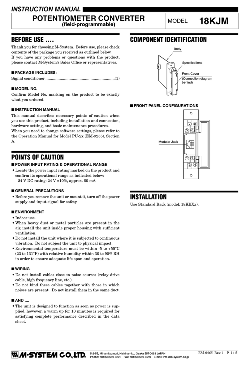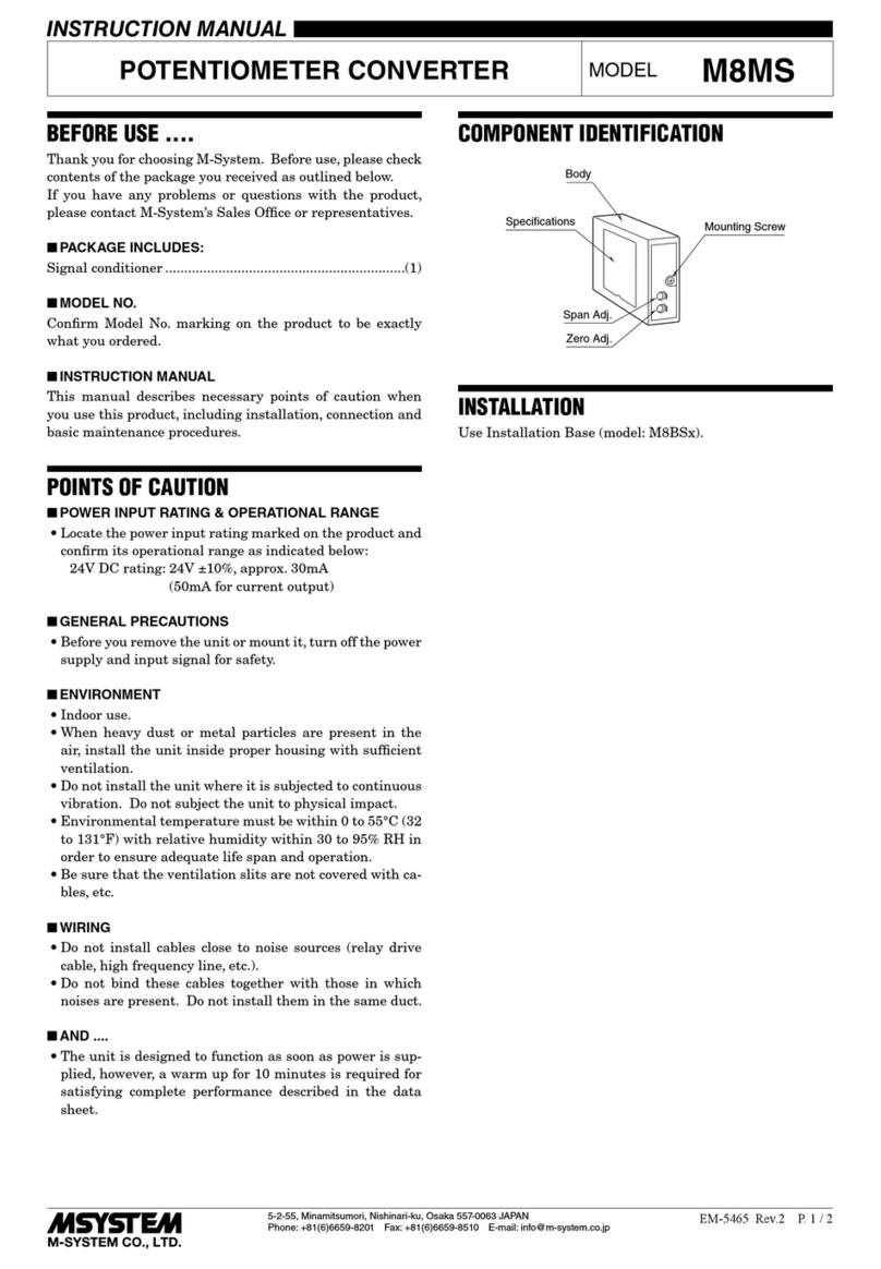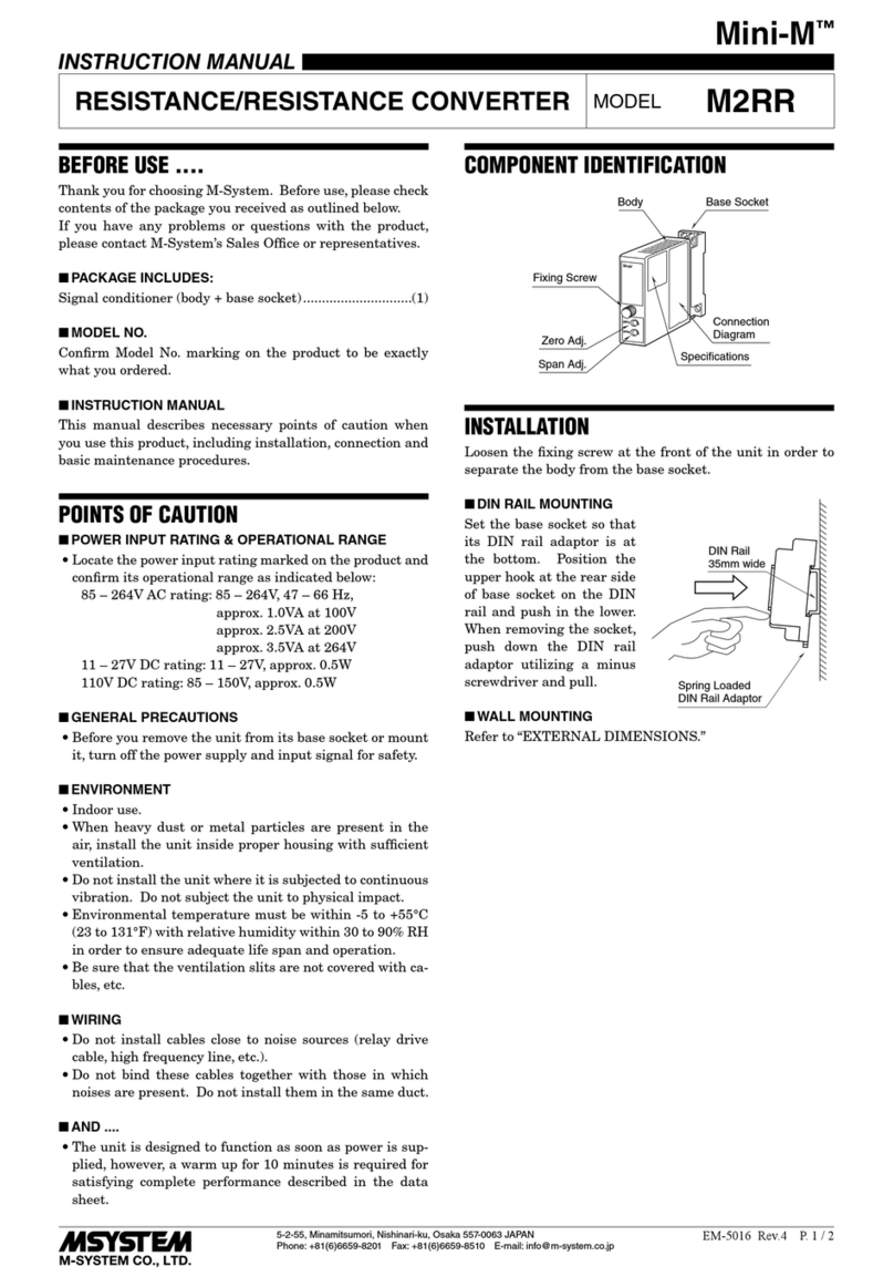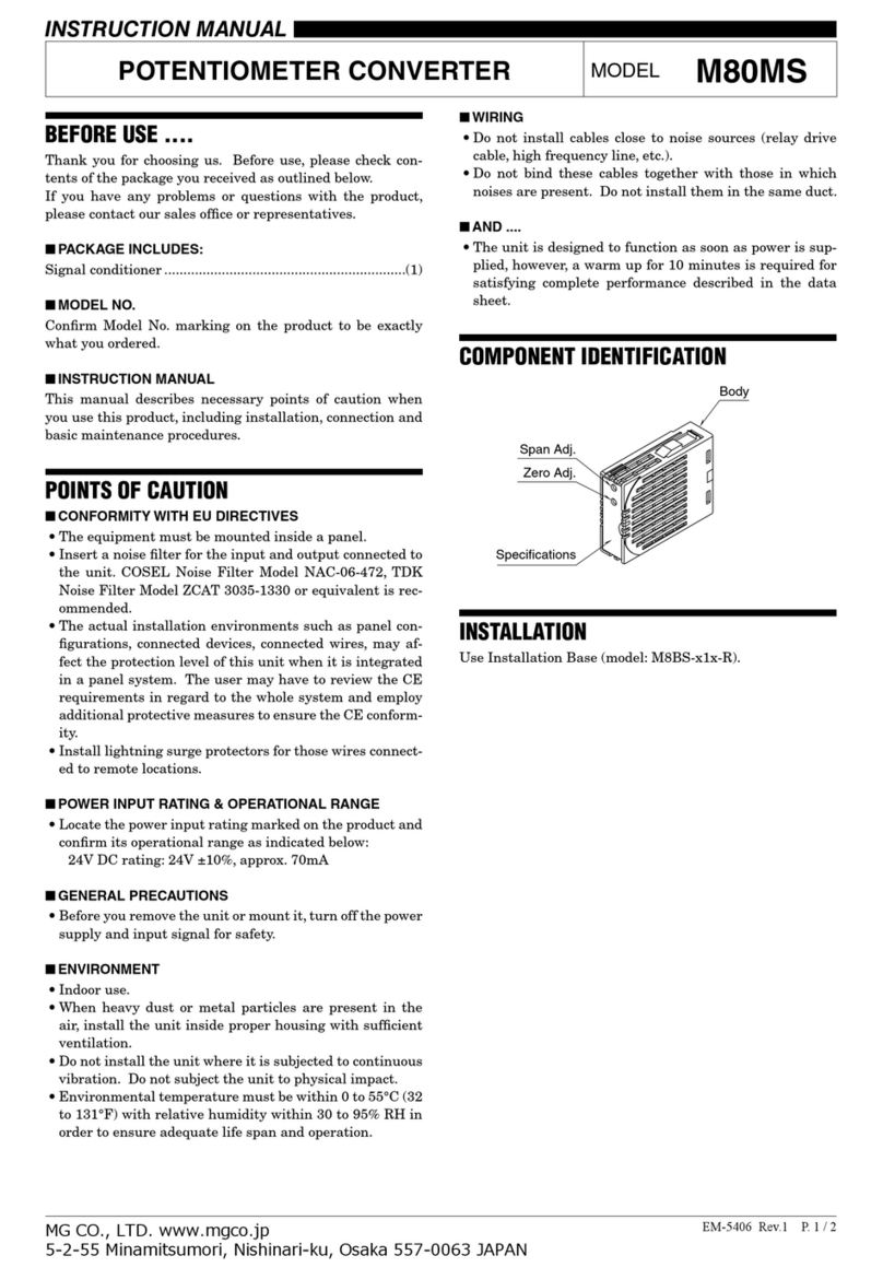
AD3V
P. 6 / 8 EM-1389 Rev.13
5-2-55, Minamitsumori, Nishinari-ku, Osaka 557-0063 JAPAN
MDF.
CODE
ITEM DATA CONTENTS DEFAULT
P/L N/A -9999 – 9999
Output display in engineering unit with ITEM 01 DATA 1 (as set in ITEM 06/07)
––
(-FFFF – FFFF) Loop test output with ITEM 01 DATA 2 (‘L’ is indicated as ITEM No.)
BCD or binary (with polarity), offset binary, two's complement, reflected binary
01 1, 2, 3 Modification code 1 : Data indication only. 1
2:All parameters are modifiable.
3:Only ITEM 24 is modifiable.
02 N/A 0 – 99 Status indication (“0” is normally indicated.) 0
0: Normal 1: Memory error 10: Out of input range -15 – 115%
03 N/A -15.0 – 115.0 Input indicated in % (of the range set in ITEM 22/23) ––
04 2 -99.99 – 99.99 Zero adjustment (%) (fine adj. of the value set in ITEM 22) 0.00
05 2 -99.99 – 99.99 Span adjustment (%) (fine adj. of the value set in ITEM 23) 0.00
06 2 -9999 – 9999 BCD Display range scaling 0% *1-1000
07 2 -9999 – 9999 Display range scaling 100% *11000
06 2 -7FFF – 7FFF Binary Display range scaling 0% *1-7FFF
07 2 -7FFF – 7FFF Display range scaling 100% *17FFF
06 2 0000 – FFFF Offset binary Display range scaling 0% *10000
07 2 0000 – FFFF Display range scaling 100% *1FFFF
06 2 8000 – 7FFF Two's complement Display range scaling 0% *18000
07 2 8000 – 7FFF Display range scaling 100% *17FFF
06 2 0000 – FFFF Reflected binary Display range scaling 0% *10000
07 2 0000 – FFFF Display range scaling 100% *1FFFF
08 2 0 – 99 Power ON-delay time (seconds) 5
09 2 0, 1, 2, 3, 4 Display code 0 : BCD with polarity (decimal) 0
1:Binary with polarity 2 : Offset binary
3:Two's complement 4 : Relfected binary
10 2 0, 1, 2, 3, 4 Available number of bits 0
0: 16 bits 1: 14 bits 2: 12 bits 3: 10 bits 4: 8 bits
11 2 0, 1, 2 Parity check 0
0: Disable 1: Enable Parity per each digit 2: Enable Parity for all digits
12 2 0, 1 Odd or even parity (Adjust the number of Hi output.) 0
0:Odd (CMOS), Even (open collector)
1:Even (CMOS), Odd (open collector)
13 2 0, 1 POL, OVF output logic 0 :
Data available at High (CMOS) or ON (open collector)
0
1:
Data available at Low (CMOS) or OFF (open collector)
14 2 0, 1 Data output logic *20:Positive (CMOS), Negative (open collector) 0
1:Negative (CMOS), Positive (open collector)
15 2 0, 1 HOLD input logic 0 : HOLD at Low or shortcircuit 0
1:HOLD at High or open circuit
16 2 0, 1 DAV output logic 0 :
Data available at High (CMOS) or ON (open collector)
0
1:
Data available at Low (CMOS) or OFF (open collector)
17 2 1 – 50 DAV output time (msec.) selectable up to 50% of the Output Rate (ITEM 20) 1
18 2 0, 1, 2, 3, 4, 5 Moving average (10 msec./sampling) 1
0: No 1: 5 samples 2: 8 samples 3: 12 samples 4: 20 samples 5: 36 samples
19 2 0.0 – 60.0 Delay buffer (seconds, 0 – 90%) 0.5
20 2 1 – 20 Output rate ‘n’ ratio (n : 1 – 20 times) 1
21 2 0, 1 – 60 Power-saving mode 0 : Continuous display 10
1 – 60 : Time before display turned off (minutes)
22 2 -1.00 – 1.00 Input code S1 0% input voltage (V) *3-1.00
23 2 -1.00 – 1.00 100% input voltage (V) *31.00
22 2 -10.0 – 10.0 Input code S2 0% input voltage (V) *3-10.0
23 2 -10.0 – 10.0 100% input voltage (V) *310.0
22 2 -30.0 – 30.0 Input code S3 0% input voltage (V) *3-30.0
23 2 -30.0 – 30.0 100% input voltage (V) *330.0
22 2 0.0 – 50.0 Input code Z1 0% input current (mA) *34.0
23 2 0.0 – 50.0 100% input current (mA) *320.0
24 3 0, 1 Reset all settings *40
25 N/A – ROM version –
*1: Of the range set in ITEM 04/05. ITEM 06 < ITEM 07. *2: ITEM 13, 15 or 16 is independent from ITEM 14.
*3: ITEM 22 < ITEM 23.
*4: Press DATA UP key and choose DATA 1. Double-click DATA DOWN key. The display shows DATA 0 after the initialization is
complete.
