Midland BASE CAMP446 User manual

BASE CAMP446
Ricetrasmettitore PMR446 multiuso
Multi-task PMR446 transceiver
-Service Manual-
Cod.603903
Via R. Sevardi 7
42124Reggio Emilia – Italy
www.cte.it

Base Camp 446
TECHNICAL DESCRIPTION
Page 1
A). GENERAL DESCRIPTION
The BASE CAMP 446 is a self-contained transceiver unit with integral
antenna intended for use as a general communication tool. It is designed to
operate on all 75 channels allocated by the CE for the licensed PMR& LPD.
This model also features a CTCSS system with 38 pre-defined, user
selectable sub-audible tones for channel quieting. The useable range, while
dependent upon terrain and other radio propagation principles, is typically ten
miles. The BASE CAMP 446 uses the maximum transmit power allowed to
help ensure the maximum communication range.
Features include : 57 Marine Channels, AM&FM Radio, Watch, and 75
PMR&LPD Channels with 38 CTCSS codes, Channel Monitor, Page and LCD
Display. The unit is equipped with an external Headset option connector.
Four AA alkaline batteries and Battery pack(NI-MH) that are readily available
in retail outlets supply operating power. An automatic power savings feature
allows the typical standby battery life to extend to more than 3 days.
B). FREQUENCY DETERMINING CIRCUITS
The fundamental frequency for both the transmitter and the receiver
local oscillators are controlled by a phase lock loop (PLL) circuit IC102
(GP214D, or equivalent). The frequency of operation of the GMRS voltage
controlled oscillator (VCO), composed of Q142, 143 operating in cascade is
phase locked to a voltage controlled crystal reference (VCXO) operating at
20.95MHz (X102).
The VCO is locked to the fundamental of the transmit signal in the transmit
mode and is locked to the receive 1st LO (Fundamental channel frequency
minus 21.4MHz) in the receive mode. The crystal reference frequency is
shared with the 2nd LO of 20.95MHz.
C). TRANSMITTER CIRCUITS
The transmitter amplifies the 0dBm signal from the VCO to
approximately 35dBm that is fed to the antenna. The transmitter is a three
stage amplifier composed of Q20,203,204 and Q205. The first two stages are
operated class A and the final is operated class B in full saturation to help
prevent unwanted amplitude modulation. The fundamental transmit signal is
fed through an elliptical low pass filter (5-pole, 2 zero) in order to suppress the
harmonics to below –50dBc. The desired frequency modulation of the carrier
is accomplished by modulating the current in the VCO directly with the
microphone audio signal. The microphone audio is conditioned with a three-
pole high pass filter at 300Hz (IC201 A,B), a hard clipper circuit (IC4 C,D) to

Base Camp 446
TECHNICAL DESCRIPTION
Page 2
limit maximum deviation to +/- 2.5KHz and a three-pole low pass or splatter
filter at 2.8KHz (IC103 A,D). The low pass filter insures that the occupied
bandwidth of the FM modulated signal meets FCC requirements under all
input conditions.
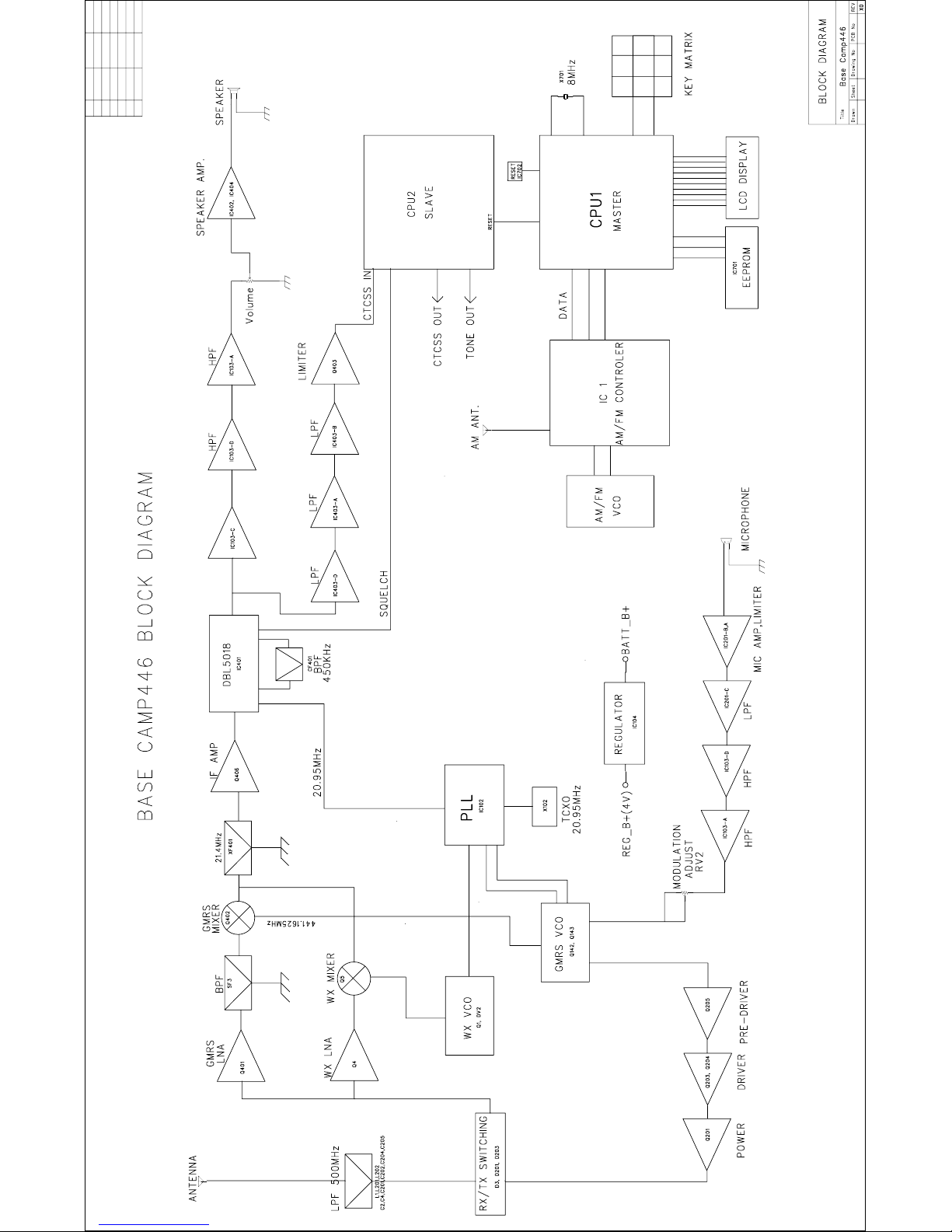
D). RECEIVER CIRCUITS
The received signal from the antenna is band limited to 600MHz by the
transmitter harmonic filter. The desired signal is fed to a low noise amplifier
(LNA – Q401) centered from 430MHz to 450MHz that provides approximately
10 dB of gain. The output of the LNA is filtered with a Band Pass filter (SF1)
with pass-band of 433MHz to 447MHz and stop band attenuation of 50 dB.
The filtered receive signal is one input to the 1st mixer (Q402), the other mixer
input (1st LO) is the output of the VCO at the desired channel frequency minus
21.4MHz. The output of the mixer is tuned to the 1st IF of 21.4MHz.
The 1st IF is transformer coupled for impedance matching to a X-tal filter
centered at 21.4MHz with a bandwidth of +/-3.75Hz. The filtered 1st IF is fed
to the 2nd mixer input of the multi-function receiver IC5. The 2nd LO (20.95
MHz) is generated by VCXO that is the reference frequency for the PLL. The
2nd mixer output of 450KHz is filtered through a 4 section ceramic filter that in
combination with the 21.4MHz X-tal filter provides approximately 50 dB of
adjacent channel attenuation. The 450KHz 2nd IF is then amplified, limited
and fed to a quadrature detector for FM demodulation. The resulting audio
output signal is band pass filtered from 300Hz to 3KHz (IC103 C,D,A) and
amplified to provide 300mW of audio power (IC402, 404). A squelch circuit is
provided to mute the receiver noise under low signal conditions. The squelch
circuit amplifies and detects noise in a narrow bandwidth at approximately 5
KHz. When the detected noise exceeds a threshold set to trigger at
approximately 9dB SINAD receive signal strength, the audio output is muted.
E). TRANSMIT/RECEIVE SWITCH
When the radio is in the transmit mode, pin diode switches D3, 202 and
D201 are both turned on (representing less than 0.7ohms). D3 and D202
allows the transmit signal to pass to the antenna and D201 shorts one leg of a
T matching network (L03, L204 and C207) to ground in the receive path. This
results in a parallel tuned circuit high impedance being presented to the
transmit signal so that the receive path does not load the transmit signal. In
the receive mode, both D3,202 and D201 are off, resulting in the antenna
signal being coupled into the receive LNA through the 50 ohm T matching
network and the unwanted load of the transmit final amplifier is reduced to
less than 1pF by D201.
F). RADIO CONTROL CIRCUIT
A microprocessor (CPU1,2) is used to control the transceiver. User stimuli is
provided through a tack switch for PTT (push to talk), along with the keypad

Base Camp 446
TECHNICAL DESCRIPTION
Page 3
for channel selection, channel monitor, receive volume, and page. Pressing
the PTT switch instructs CPU1,2 to switch to the transmit mode. This is
accomplished by loading the proper channel counter information through a 3-
wire serial link to the PLL IC (IC102), turning on power to the PLL and VCO,
microphone and transmit audio circuits and the transmit RF amplifiers.
Pressing the call switch causes the microcontroller to transmit a warbling tone
for approximately 3 seconds on the current channel selected that is used to
notify another person with GMRS radio that you wish to communicate.
Pressing the channel Up/Down buttons (active in receive mode only) instructs
U5 to increment or decrement respectively the channel frequency by one
channel from the channel previously selected.
In receive mode the microcontroller periodically switches on the VCO and
receiver power and checks for a valid received signal by monitoring the
squelch circuit output. If a valid signal is present, the audio output is turned
on and receive power is maintained for the duration of the valid signal. If the
valid signal is removed or no valid signal was present, the microcontroller
removes power from the VCO and receiver, waits for approximately 100 ms
and then checks again. This periodic cycling of the power to the receiver
circuits results in a much longer battery life vs. leaving power on continuously.
The total period of the cycling is selected such that the worst case delay in
‘seeing’ a valid receive signal is not disruptive to normal two-way voice
communications.


Main PCB_X1 version BS446_X1 1
Sub PCB 1 for Function botton 1
Sub PCB 3 for Light LEDs 1
Sub PCB 2 for Power/Volume/Tone control switch 1
Q203 BFQ67W Transistor Chip 1
Q204 BFQ67W Transistor Chip 1
Q205 BFQ67W Transistor Chip 1
C201 0.5P Chip cap 0402 NP0 1
C2 1.5P Chip cap 0402 NP0 1
C109 100P Chip cap 0402 NP0 1
C11 100P Chip cap 0402 NP0 1
C110 100P Chip cap 0402 NP0 1
C111 100P Chip cap 0402 NP0 1
C112 100P Chi
p
ca
p
0402 NP0 1
Ref.No Items Description Q'ty
C112
100P
Chip
cap
0402
NP0
1
C114 100P Chip cap 0402 NP0 1
C116 100P Chip cap 0402 NP0 1
C117 100P Chip cap 0402 NP0 1
C12 100P Chip cap 0402 NP0 1
C121 100P Chip cap 0402 NP0 1
C123 100P Chip cap 0402 NP0 1
C124 100P Chip cap 0402 NP0 1
C128 100P Chip cap 0402 NP0 1
C130 100P Chip cap 0402 NP0 1
C132 100P Chip cap 0402 NP0 1
C134 100P Chip cap 0402 NP0 1
C137 100P Chip cap 0402 NP0 1
C138 100P Chip cap 0402 NP0 1
C140 100P Chip cap 0402 NP0 1
C141 100P Chip cap 0402 NP0 1
C144 100P Chip cap 0402 NP0 1
C149 100P Chip cap 0402 NP0 1
C156 100P Chip cap 0402 NP0 1

C157 100P Chip cap 0402 NP0 1
C161 100P Chip cap 0402 NP0 1
C162 100P Chip cap 0402 NP0 1
C164 100P Chip cap 0402 NP0 1
C166 100P Chip cap 0402 NP0 1
C18 100P Chip cap 0402 NP0 1
C182 100P Chip cap 0402 NP0 1
C213 100P Chip cap 0402 NP0 1
C216 100P Chip cap 0402 NP0 1
C217 100P Chip cap 0402 NP0 1
C221 100P Chip cap 0402 NP0 1
C222 100P Chip cap 0402 NP0 1
C223 100P Chip cap 0402 NP0 1
C227 100P Chip cap 0402 NP0 1
C231 100P Chip cap 0402 NP0 1
C232 100P Chi
p
ca
p
0402 NP0 1
C3
00
C p cap 0 0 0
C234 100P Chip cap 0402 NP0 1
C237 100P Chip cap 0402 NP0 1
C241 100P Chip cap 0402 NP0 1
C243 100P Chip cap 0402 NP0 1
C247 100P Chip cap 0402 NP0 1
C250 100P Chip cap 0402 NP0 1
C252 100P Chip cap 0402 NP0 1
C254 100P Chip cap 0402 NP0 1
C255 100P Chip cap 0402 NP0 1
C26 100P Chip cap 0402 NP0 1
C29 100P Chip cap 0402 NP0 1
C30 100P Chip cap 0402 NP0 1
C33 100P Chip cap 0402 NP0 1
C40 100P Chip cap 0402 NP0 1
C401 100P Chip cap 0402 NP0 1
C402 100P Chip cap 0402 NP0 1
C403 100P Chip cap 0402 NP0 1
C405 100P Chip cap 0402 NP0 1

C407 100P Chip cap 0402 NP0 1
C408 100P Chip cap 0402 NP0 1
C41 100P Chip cap 0402 NP0 1
C42 100P Chip cap 0402 NP0 1
C422 100P Chip cap 0402 NP0 1
C43 100P Chip cap 0402 NP0 1
C44 100P Chip cap 0402 NP0 1
C442 100P Chip cap 0402 NP0 1
C448 100P Chip cap 0402 NP0 1
C465 100P Chip cap 0402 NP0 1
C472 100P Chip cap 0402 NP0 1
C5 100P Chip cap 0402 NP0 1
C51 100P Chip cap 0402 NP0 1
C52 100P Chip cap 0402 NP0 1
C6 100P Chip cap 0402 NP0 1
C612 100P Chi
p
ca
p
0402 NP0 1
C6
00
C p cap 0 0 0
C7 100P Chip cap 0402 NP0 1
C708 100P Chip cap 0402 NP0 1
C709 100P Chip cap 0402 NP0 1
C711 100P Chip cap 0402 NP0 1
C712 100P Chip cap 0402 NP0 1
C713 100P Chip cap 0402 NP0 1
C714 100P Chip cap 0402 NP0 1
C715 100P Chip cap 0402 NP0 1
C717 100P Chip cap 0402 NP0 1
C76 100P Chip cap 0402 NP0 1
C8 100P Chip cap 0402 NP0 1
C9 100P Chip cap 0402 NP0 1
C99 100P Chip cap 0402 NP0 1
C413 10P Chip cap 0402 NP0 1
C461 120P Chip cap 0402 NP0 1
C153 12P Chip cap 0402 NP0 1
C457 150P Chip cap 0402 NP0 1
C1 15P Chip cap 0402 NP0 1

C214 15P Chip cap 0402 NP0 1
C624 180P Chip cap 0402 NP0 1
C72 18P Chip cap 0402 NP0 1
C14 1P Chip cap 0402 NP0 1
C220 1P Chip cap 0402 NP0 1
C414 1P Chip cap 0402 NP0 1
C152 220P Chip cap 0402 NP0 1
C629 220P Chip cap 0402 NP0 1
C125 22P Chip cap 0402 NP0 1
C133 22P Chip cap 0402 NP0 1
C15 22P Chip cap 0402 NP0 1
C16 22P Chip cap 0402 NP0 1
C39 22P Chip cap 0402 NP0 1
C700A 22P Chip cap 0402 NP0 1
C700B 22P Chip cap 0402 NP0 1
C17 2P Chi
p
ca
p
0402 NP0 1
C
C p cap 0 0 0
C622A 2P Chip cap 0402 NP0 1
C120 33P Chip cap 0402 NP0 1
C126 33P Chip cap 0402 NP0 1
C19 33P Chip cap 0402 NP0 1
C24 33P Chip cap 0402 NP0 1
C705 33P Chip cap 0402 NP0 1
C706 33P Chip cap 0402 NP0 1
C719 39P Chip cap 0402 NP0 1
C151 3P Chip cap 0402 NP0 1
C245 3P Chip cap 0402 NP0 1
C228 47P Chip cap 0402 NP0 1
C625 47P Chip cap 0402 NP0 1
C622 4P Chip cap 0402 NP0 1
C74 4P Chip cap 0402 NP0 1
C135 5P Chip cap 0402 NP0 1
C159 5P Chip cap 0402 NP0 1
C207 5P Chip cap 0402 NP0 1
C215 5P Chip cap 0402 NP0 1

C219 5P Chip cap 0402 NP0 1
C224 5P Chip cap 0402 NP0 1
C410 5P Chip cap 0402 NP0 1
C718 68P Chip cap 0402 NP0 1
C160 6P Chip cap 0402 NP0 1
C415 6P Chip cap 0402 NP0 1
C432 6P Chip cap 0402 NP0 1
C38 7P Chip cap 0402 NP0 1
C604 7P Chip cap 0402 NP0 1
C246 82P Chip cap 0402 NP0 1
C253 82P Chip cap 0402 NP0 1
C154 8P Chip cap 0402 NP0 1
C22 8P Chip cap 0402 NP0 1
C148 9P Chip cap 0402 NP0 1
C165 0,001 Chip cap 0402 X7R +/-10% 1
C187 0,001 Chi
p
ca
p
0402 X7R +/-10% 1
C8
0,00
C p cap 0 0 / 0%
C20 0,001 Chip cap 0402 X7R +/-10% 1
C225 0,001 Chip cap 0402 X7R +/-10% 1
C249 0,001 Chip cap 0402 X7R +/-10% 1
C31 0,001 Chip cap 0402 X7R +/-10% 1
C36 0,001 Chip cap 0402 X7R +/-10% 1
C408A 0,001 Chip cap 0402 X7R +/-10% 1
C411 0,001 Chip cap 0402 X7R +/-10% 1
C412 0,001 Chip cap 0402 X7R +/-10% 1
C417 0,001 Chip cap 0402 X7R +/-10% 1
C479 0,001 Chip cap 0402 X7R +/-10% 1
C48 0,001 Chip cap 0402 X7R +/-10% 1
C62 0,001 Chip cap 0402 X7R +/-10% 1
C71 0,001 Chip cap 0402 X7R +/-10% 1
C720 0,001 Chip cap 0402 X7R +/-10% 1
C75 0,001 Chip cap 0402 X7R +/-10% 1
C441 0,0012 Chip cap 0402 X7R +/-10% 1
C447 0,0012 Chip cap 0402 X7R +/-10% 1
C628 0,0015 Chip cap 0402 X7R +/-10% 1
Other manuals for BASE CAMP446
1
Table of contents
Other Midland Transceiver manuals

Midland
Midland Atlantic User manual

Midland
Midland G-11 Manual

Midland
Midland 8011869177026 Manual

Midland
Midland D-200 User manual

Midland
Midland 70-1545 User manual

Midland
Midland 13-513 User manual

Midland
Midland PMR 446 G5 User manual

Midland
Midland CT 890 User manual

Midland
Midland M-Mini Manual

Midland
Midland M-30 Manual

Midland
Midland G8E-BT Manual

Midland
Midland G18 Manual

Midland
Midland 70-066 User manual

Midland
Midland M24 Plus User manual

Midland
Midland BASE CAMP User manual

Midland
Midland CT 710 User manual

Midland
Midland 77-104XL User manual

Midland
Midland 75-440 User manual

Midland
Midland 248XL Manual

Midland
Midland CT 890 Manual