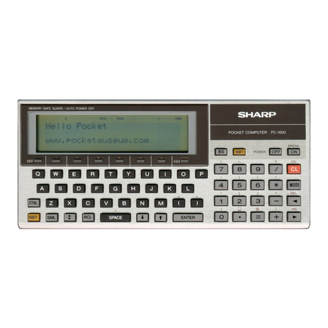
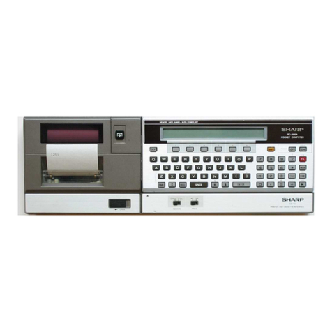
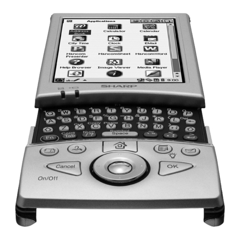
Sharp PC-1285 Assembly instructions

This document has been published to be
used for after sales service only.
The
contents are subject to change without
notice.
RAMcard
CE-21
OM
(2KB)
CE-211
M
(4KB)
CE-212M (8KB)
CE-2H16M (16KB)
CE-2H32M (32KB)
SHARP CORPORATION
CE-140F pocket
disk drive
CE-126Pprinter and
cassette
inter
f
ace
eg DODOO
DODOO
CJDCJD DODOO
DODD DODOO
•CJCJ ODDO
CE-124cassette
interface
,
..__I
_ ___.
PC-1285pocket computer
CE-120P
Printerwith
Cassette interface
Dot matrix liquid crystal display (2-line 24-
digits)
8-bit CMOS CPU
Calculation capacity: 12digits
Calculator functions: Add, subtract, multip-
ly, divide, constant, percentage, add-on,
discount, power raising, reciprocation,
memorycalculation, etc.
6VDC, lithium battery cells (CR2032x 2)
0.03W
Approx
.
120 hours of continuous use (with
CE-212M) under normal conditions
(based on
1
O
minutes of arithmetic opera-
tion or program execution and 50 minutes
of display per hour at a temperature of
2o·c).
Life may vary depending on the operating
conditions and the type of battery used.
o·cto4o·c
135(W) x
141
(D) x 9.6(H)mm (opened)
135(W) x 70.5(D) x 19.2(H)mm (closed)
1759 (batteries included)
(APPLICATIONONLY)
Weight:
Operating temperature:
Dimensions:
Powersupply:
Powerconsumption:
Battery life:
Math operations:
CPU:
Display:
POCKET COMPUTER
MODEL PC-1285
CODE: OOZPC1285SM/E
CE
-
127R microcassette
tape recorder
CE
-
152 cassette
tape recorder
System diagram
PC-1285
Model:
2. SPECIFICATIONS
The PC-1285
is
an application only version of the PC-1280which has
a
simila
r circuitries and functions as those of PC-1280.While the
PC
-
1280 has an internal 8KB RAM, the PC-1285
is
not and may not
operate without a RAM
card
.
An internal RAM backup battery and an
internal RAM protect switch are therefore not used
in
the PC-1285.
1.
INTRODUCTION
Keyboard layout
SERVICE
MANUAL
SHARP -
PC-1285
,..
.
-2-
E
O
O
co
o
8000
4000
2800
20
00
I
n
ternal
RO
M
BK
B
DI
SP
& port
I
I
S
ystem
RO
M
I I
1
6
K
BX
8
BANK
I I
I I
BANK
R
O
~
R
I
I
-
I
R 7
0
------
0
-
-----
0
----
-
-
A
OO
~-------
--+
D3 D2 DI
DO
0 0 0
K
S
I
I
0
0
0
K
S
8
I
K
S
!
-
KS
8
0000
38
00
Po
rt
wri
t
e
C
E
3A
O O
Port
w
r
ite C
E
3
C
OO
Memory map
3EOO
Key stroke
w
r
ite
CE
4000
3600
RAM bank add
r
ess
ROM bank
C
E
3400
3 2
O O
Caution PON latch
wr
i
te
CE
3 0 0
O
Low batt
e
ry
l
atch
C
E
conv
e
rsion
2EOO
G
.
APOB
2COO
D
o
~
o
PC-1470
U/
7
5
P
OB
~~~~~~~
I
P
C
-1280
A13sentonPOB
P
C
-1
285
D
I
SP
2
2A
O
Or--
-
--_,
P
O
I
P
0
2
P03
L===
:'..
P04
D
I
S
P
I
P05
P06
P07
~---
-
POB
2800~-
--
....,
5
.
MEMORY MAP
A
p
rog
ram
creat
e
d on the
p
ro
g
r
a
mma
ble
uni
t can be loaded
ont
o
the
PC-12
85 in
eit
her
o
f
th
e
fo
ll
ow
i
n
g
wa
y
s
:
(1)
U
s
ing
th
e
progr
a
m
st
o
r
ed
RA
M card
(
2
)
To
l
o
a
d
prog
r
a
m fr
o
m
t
he
c
assett
e
tap
e or
m
icr
o
c
a
ssette
tape
.
I
n
t
h
i
s
ca
se
,
the
foll
ow
i
ng
op
ti
on
G)
and
®
a
r
e
requ
ired
.
G)
C
E
-
126
P
p
rin
ter
/
cassette
i
n
t
erface
o
r
CE-1
24
cassett
e
i
n
ter
-
face
®
CE
-1
52
cassett
e
tape recorder
o
r
C
E
-
1
2
7
R
m
i
c
roc
as
sette
ta
pe
reco
r
der
(
3
)
To load
p
r
ogra
m
f
r
om the
2
.
5
"
pocket
d
isk.
I
n
thi
s
ca
s
e
,
t
he
fol
-
lowing option
i
s
requ
i
red
.
CE
-
140F (pocket
d
i
sk drive)
(4) To load program directly from another pocket
comput
er.
In
th
is
case
,
the following cable
opt
i
on
i
s
required.
EA
-
128C
NOTE:
Note the following when loading the RAM card
w
i
th the program
created or
ed
i
ted on the
PC
-
1280
.
(
1
)
Set the PC-1280
i
n
the
MEM$=
"
1
"
when creating or
ed
i
ting the
program
.
(Execute SETMEM "1"
I
ENTER
I
.)
(2) Erase reserve data by
PC
-
1280 before
load
i
ng to PC-1285.
Do the following operation to erase
.
ISHIFTI IBASICI
.
..
Set
in
the reserve mode (RSV symbol on)
[HJ~
&YI
IENTERI
...
Erasereserve
data
.
4.
L
OADING PROGRAM
The above values are at the room temperature of
2o
·
c
and may vary
depending on conditions.
(NOTE) Current
sh
ou
ld be measured
w
i
th a RAMcard loaded.
45µA max.
450µA
max
.
Cur
r
ent consumption when
PC
-
1285 OFF
Current consumption when
PC
-
1285 ON
(
w
i
t
h d
i
splay on)
Current consumption
Term
i
nal
voltage:
6
.
0V
Capacity
:
170mAH
PC-1285 power Lithium battery
supply CR-2032 x
2
pcs
3. BATTERY LIFE AND CURRENT
CONSUMPTION
..
PC
-
1285

8
XIN
I
n
Cassette signal
i
n
p
ut
9
XON In
ON
/
BRK key
input
,
normally
pu
ll
ed
down low.
10 XO
U
T Out
Cassett
e
signa
l
a
nd
buzzer
s
i
gna
l
o
u
tput
1 1
DIS
O
u
t
L
CD
d
ri
ver
con
t
ro
l
s
i
g
n
a
l,
high
du
rin
g
disp
l
ay
i
ng
1
2
HA
Ou
t LCD
dr
iv
er
sync
c
l
o
c
k
1
3
IA8
In/
Out Key
inpu
t/
key strobe
14 IA7
In
/
Out Key
inpu
t/
key
s
t
robe, low
d
uri
ng
I
I I
standby
I
20
IA1
In/Out Key
i
nput/key strobe, low
du
ri
ng
standby
21
IB8
-
Not used
22 IB7
-
Not used
23 IB6
-
Not used
24
I
B5
In
11
pin ACK
(acknowled
ge
o
n
1
1
pin
i
nterface)
25
I
B4
I
n
t
t
-
pin DIN (data
i
nput on
t
t
-
pin
i
nterface
)
26
183
In
t
t
-
pin DOUT (data
inpu
t on t
t
-
p
in
in
t
erface
)
27
I
B2
In
t
t
-
pin 102(data
i
np
u
t on t
t-
pin
interf
a
ce)
28
IB1
In
t t-pl
n
101
(
d
ata input on
1
1-
pin
in
te
rf
a
c
e
)
29
V
M
In
L
CD
d
riv
e
powe
r
30
V
A In
L
CD
d
rive power
31
GND
I
n
(
+
)
s
u
pp
ly
32
H
1
O
ut
L
CD
b
ack
p
l
a
t
e
signal, 4-level pulse
I I
I
d
ur
in
g
di
splay
i
ng
(1
/
14 duty)
I
45 H14 Out LCD
backp
l
ate
signal
,
4-level pulse
du
r
ing displaying
(1
/
14 duty)
46,47
H
1
5
,H16
-
N
o
t used (because
o
f
1
/14 duty)
48 VB
In
LCD
dr
i
ve
p
ower
,
hi
gh
d
uring
standby
49 VD
I
S
In
LCD drive
power
,
h
i
gh during
standby
50
vcc
I
n
LCD
d
ri
ve
p
ower
,
h
i
gh
du
r
i
ng
standby
51
voe
Ou
t LCD
dr
i
v
e
power
,
hi
gh
durin
g
standby
52
V
GG
In
(-)s
upp
l
y
53
08
In/
Out Databus
07
,
norma
ll
y
h
i
gh
I
I
I
i
mpedance
I
60
0
1
In
/
O
ut
Dat
a bus
DO
,
no
rm
a
lly high
im
peda
nc
e
6
1
F0
5
O
u
t
Ga
te
a
rr
ay
ch
i
p
enable (CF)
62
F
0
4
Ou
t
R
OM
c
h
ip
enab
l
e
6
3
F
03
O
ut
R
AM
ca
r
d
bank
se
l
ect
(
BA
)
6
4 F02
-
Not
u
se
d
6
5
F
0
1
O
ut
Lo
w battery
d
et
ect
,
h
i
gh
im
p
e
danc
e
d
ur
i
ng
s
t
andby
66
B08
Ou
t
Add
r
e
ss
bus A
15
,
h
i
g
h
durin
g
I I I
st
a
n
dby
I
7
3
B0
1
O
u
t Address bus A
15
,
high
duri
n
g
sta
n
dby
7
4
A08
O
ut Addressbus A
15
,
highduring
I I I
standby
I
80
A02
Out Address bus A1, highduring standby
-
PC-12
85
-3
-
Pin Signal
I
n/
O
ut Description
(
Standby-power off)
No
.
name
1
A01
O
u
t
Address
bu
s
A
O,
h
i
g
h
du
ri
ng
st
andby
2
Rfiii
O
u
t
Wr
i
t
e
c
l
ock
,
no
r
ma
ll
y
h
i
gh
3
cp
AL Out Address
la
t
ch
.
C
l
oc
k
u
sed
t
o
la
tc
h
t
he
a
ddress of the LCD
d
ri
v
e
r.
4
T
ES
I
n
Test pin, normally
l
ow
5
cp1
In Oscillator input
6
cpo
Out Oscillator output
7 RES
I
n
Reset
input
,
resetwith a high
sta
t
e
of
s
i
gnal.
7
-
1
.
CPU (SC61860A38)
7. LSI SIGNAL DESCRIPTION
[Fi
g
.
3
]
Q
b.._
_
L_
_
~
L_ _
___L_.,
_
Act
i
on
o
f the
vo
l
tage
de
te
ct
IC
[Fi
g.2]
~
Cl)
_
CAU
sig
n
a
l
lev
e
l
Ol
~
-+
- -
--
STO
Ps
i
g
n
a
l
;:,
S
ymbol ON
le
vel
a.
Cl.
L__ _
::J
(J)
2
.
0V
-
O<-
-~-~~-
---t--+
-'P
OUT
(
V
)
GA
CA
U
------'
(N-chopen)
R2
CPU
F
Oi
(P
-
ch
open)'!--
---
~
RI
[Fi
g
.1]
D
I
!
As
t
he
PC
-
1285
i
s
p
r
ovid
e
d with a low battery detect circuit
li
k
e
t
he
PC
-1
280
,
t
hi
s
sec
ti
o
n
de
s
c
ri
b
e
s about
it
s
f
u
n
ctio
n.
(
Note that the parts
l
ocat
i
on num
be
rs do
no
t always
co
i
ncide with
th
o
se
in
th
e
ac
tu
a
l
c
ircu
i
t
d
i
agram
.)
A
s shown
i
n
t
he
figur
e
be
l
ow
,
t
he
output from the low
batte
ry
de
t
ect
IC
,
LB
I
C (MN1280)turns
h
i
gh when the input voltage VIN
r
i
ses above
the detect
vol
t
age level VD, or turns to
l
ow when VIN drops below
VD.
For
bo
t
h
s
i
gnal
le
v
e
l
s of CAU and STOP are
mo
n
itored by a single
IC
,
LBIC
(MN1280
),
the
p
i
n
2 input
i
s divided by
R1
and
R2
,
and R2
is
tu
rned on and off with
ga
t
e
array CAU
.
As
F
i
g.3
shows
,
when
t
he
supp
l
y voltage goes below
t
he
l
eve
l
of the
CAU
s
i
gnal
,
the BATT symbol
i
s
se
t
act
i
ve
.
When
i
t goes
fu
rt
he
r
down below the
leve
l
of the
signa
l
STOP
,
the symbol
i
s turned
off
.
To
chec
k the level of the signal CAU,
t
he state of
th
e
line LB is
i
nter
-
r
oga
t
ed by
sett
i
ng CAU
l
ow (active
).
I
f LB
i
s
a
t a low level, the
s
y
mbo
l
is
act
i
vated
.
After sensing the CAN level, the CAN line is set off
(h
i
g
h
impedance)
.
When CAU is turned
off
,
the output changes from low to
high as the voltage on pin 2
i
ncreases as there is no more
r
es
i
stance
d
i
v
i
s
i
on. As LB is interrogated again,
t
he levelof STOP
i
s
sensed
.
In
the standby mode,
F01
of
t
he CPU and CAU of the gate array are
set high impedance.
011
is employed to compensate for a battery
voltage drop between the standby and
ope
r
ating
.
Upon detection of
the STOP
level
,
bo
th the
ON/
B
RK key and the
RES
E
T switch are
dis
-
abled.
6. LOW BATTERY
D
ETECT CIRCUIT

1.
A
s s
h
ow
n
i
n
the
fi
gu
r
e
above
,
i
nsert
yo
u
r
na
il
i
n
t
he clearance
be
-
tween CAB-A and
CAB
-
C near the
h
inge and push
i
t down
i
n
the
a
r
row dire
c
tion to disengage the latch C at two locations
(Fig
.
2
).
1
.
Eng
a
ge
t
he
la
t
ch
A
,
Fig
.
2
,
as shown
i
n
Fig.
1
G)
2. Engage the latch
B,
Fig.2.
3
.
Engag
e
the latch
C
,
F
i
g
.
2
,
as shown
i
n
Fig.1®
How
to
remove CAB-A
[
F
i
g.2]
L
at
ch
B
[F
i
g
.1
]
®
/~=::::::::::::::=::::::::::::::~~
~==~~~~~
=
~
~
I
C
AB-B
CAB-A
8-1.Rem
o
val
an
d
in
stallati
on
of
C
A
B-
A
Hintsto
latch CAB-A
with
CA
B
-
B
CA
B
-
A
C
AB-D
Each
cab
i
net
i
s
calle
d as
follows
:
D
isplay
sid
e
bottom
c
ab
inet:
C
A
B
-
A
Displaysidetop
c
a
b
in
e
t: CA
B
-B
Keyboardside bottom
c
ab
in
e
t:
CA
B-C
Keyb
o
ard
s
ide top
c
ab
i
n
et:
C
A
B-
D
8. SERVICE PRECAUTIONS
-
4-
P
i
n
S
i
gna
l
In/
Ou
t
D
escri
p
t
io
n
No
.
n
ame
1
BA
In
Ban
k
selec
t
2 CE
I
n
C
h
ip enable
3
D
C
O
In
D
a
ta bus
I
I I
I
6
D03 In
D
ata bus
(
7
GND In
(
-
)supply
8
P
0
1
Out 11-pin
101
(P-channe
l
open output)
9
P02
Out
11
-
pin 102
(P-channe
l
open output)
10
P
0
3 Out 11-pin DOUT (P-channel
op
en
output)
11
P04
Out
11
-
pin DIN
(P
-
channel open output)
1
2
P05
Out 11-pin BUSY
(
P-
channel open
output)
13
N
C
-
Not used
14 SLTB Out
N
o
t used
15 AS3B Out Not used
16 AS1
O
u
t System ROMA14 and RAM A
11
17 AS2 Out System ROMA15 and RAM A12
18 AS3 Out System ROMA16 and RAMA13
19 AF15 Out RAMcard slot
A
1
5
20 AF16 Out RAMcard A16
2
1
SLT1
O
ut RAMcard
s
l
ot chip
ena
ble
22 SLT2 Out InternalRAM chip
enab
l
e
23 DSP1 Out DISPCHIP1chip
en
able
24 DSP2 Out
DISPCH
I
P2 chip enab
l
e
25 RESO Out Resetoutput
t
o
CPU RESET
li
ne
,
normally low
26 KON
O
ut
ON
/
BRK
ou
t
pu
t
t
o
C
PU KON
l
in
e
,
n
orma
lly
l
ow
27 LB
In
Low
b
att
e
ry
de
tec
t,
l
ow at low
batte
ry
28 RES1
I
n
Reset
input
,
normally pulled down
29 BRK
In
ON
/
BR
K
k
ey
i
nput
,
normally pulled
down
30 Voo
In
(
+)s
u
pply
3
1
GND In
(-)supp
l
y
32 CAU Out Low battery symbol
act
i
vat
i
ng
voltage
det
e
ct
li
ne, high
i
mpedance
after
ac
ti
vation of
symbo
l.
33
KS
1
Out Key strobe
(
P
-
channel open
outpu
t)
I I I I
40 KS8 Out Key strobe
(
P-channel open
output
)
41
R/W
In
Write clock
42 A9
In
Add
r
ess
b
u
s
I
I
I I
48 A15 In
A
ddress bus
7
-2. Gate array (LZ92K41)
~
PC
-
1285

(Fig
.
3)
(5) Insta
ll
the
memo
r
y PWB unit
,
Fig
.
2
,
over the keysheet and insert
t
he FPC
term
i
na
l
onto the
gu
i
de
p
in
s on CAB-B.
NOTE
:
Do
no
t install the memory PWB
o
n
to the
g
u
ide pins
yet.
(
6) Install the mask
sheet
,
then the
fix
i
ng rubber on the
f
ace of the
cabine
t,
after which
fo
l
d back the ear of the FPC to fit it on
th
e
guide pin
(Fig
.
3
.
)
(7)
P
osi
tion the sealing
a
n
g
l
e
t
o the guide
pi
n
s
o
n
CAB-B
a
nd
secur
e
i
t
w
it
h
fou
r
sc
rews
.
N
OT
E:
Tig
ht
en the
t
w
o
in
ner
s
crew
s
fi
r
st,
t
h
en
tw
o
o
t
h
er
scre
w
s
.
G
uid
e
pin
/
(Fig.2)
FPC
(Fi
g
.
1)
C
A
B
-
D
(
ke
y
b
oa
r
d
s
i
de
t
op
c
ab
inet)
Lower
h
alf
ke
y
sh
e
et
M
as
k sheet
..
PC
-
1285
-5-
8-4.
In
sta
llin
g
PWB
,
keysheet
,
etc
.
(1)
A
ss
em
b
l
e
t
he
ma
s
k sheet,
t
h
en
t
h
e
ma
i
n
PWBonto CAB
-
B
.
(2)
Inse
r
t the
ru
b
ber key in
C
A
B
-D
,
t
hen
inst
a
ll
t
he
upp
er
h
al
f
o
f the
ke
y
s
hee
t.
Pos
i
tio
n
t
h
e
s
hee
t onto the
gu
i
de
p
in
s and key
s
heet
ho
l
d
in
g
pin
s
.
(3)
In
s
ert the key spacer by
pos
i
t
i
oning it to the guide pins.
(
4
)
Fold back the
low
e
r
half of the key sheet and fit the terminal onto
t
he guide
p
i
ns on
CAB
-B
.
NOTE:
A
t
th
i
s
point
,
the lower half of the key sheet should notyet be
on the guide pins or holding pins, and the fold line should be
left
loose
.
Knob
(?1 ll
Contact
Q;Y'
*
For the contact
is
secured on the knob at two
l
ocations, it has to be
i
nstalled on the location as in the
figure
.
8
-
3.
Ins
ta
lli
ng
t
h
e
c
ont
a
ct
to the
L
OCK s
w
i
t
ch
knob
Pin
o
nC
AB
-
D
~
/
/,?
(k
e
yboa
r
d
si
de
to
p
CAB
-
c
/
{(
c
abi
net)
/
H
ole
i
n
CAB
-
C
(key
boar
d
side
bott
o
m
c
abinet)
*
The
p
i
n
m
u
st be proper
l
y
a
n
d
firml
y
e
n
g
aged in the hole.
l
t
~J
Latch
~[
[
L
at
c
h
I
8-2.
Installing
CAB-C
*
Makesure that
t
h
e
p
i
n
i
s properly engaged
i
n
the hole.
*
W
he
n
l
atc
hi
ng
CAB
-
C
w
i
th CAB
-
D
,
pus
h
CAB
-
C
all
t
he way in
th
e
arr
owhead A to achieve
fi
rm engageme
n
t.
Us
e
the spec
i
al
tool to
tight
enthe
screws
.
2.
D
o the reverse sequence to remove the latches.
CAUTI
ON: When
r
emoving CAB
-
A
,
be
c
areful not to separate
t
he
sta
ti
c
t
ape.

8-10
.
Display
test
Items
req
ui
red for disp
l
ay
c
h
eck
:
•
PC-12
8
0
(for
p
r
ogram
entry
)
•
Half
-
size RAMcard (fortest)
•
PC-
1
285 to be tested
Th
e
contents of
bo
t
h
PC-1280 and the RAM card will be
l
os
t during
t
he
t
est.
(1)
Set
t
he RAM card in the PC-1280 and do ALL RESET.
(
2) Enter SETMEM"1"
[:;;D
.
8
-
9. Displayside cabinet and keyboard side
cabinet
These two cabinets are held together
wi
t
h
a spring
pin
.
To replace
ei
ther
o
n
e only, it
may
be
po
s
sible to scrape the cabinet with
t
he
cut
-
te
r
a
nd
t
o
r
emove
t
he spring pin
w
it
h
a
pa
i
r of pliers
,
but the
pin
,
once
pulle
d
out
,
cannot be
re-used
.
Le
n
gth PWB
un
it
J1
140
Ma
i
n
PWB
J2 105
J3
12
7
Mem
ory PWB
•
Pro
v
i
di
ng
j
umpe
r
~
I
.
8
~I
w
•
Pr
o
vide
t
he
f
o
ll
ow
i
ng
1
O O
Q
r
esisto
r.
• The capacitor
i
nserted to the 11-pin
connect
o
r must be installed in
the following
m
a
nner.
8-8
.
Hin
t
s and
tips
• Any
p
arts must be closely
a
ttached on the PWB with
so
l
de
r.
• When replacing
LSls
,
use the ALUMIT KR19RAM
solder
.
(See
Service
In
formation PS-009.)
• See the figure below for the
i
nstallation of a
0
.
1uF
in
sert
ed across
v
-
the KON (pin 26) of
th
e
ga
te
a
rray and the VGG
s
ide
o
f a
0
.
0
33uF.
-
6
-
The contents of the memory will be erased
w
i
th the
follow
i
ng proce-
dure.
(1) Insertthe RAM
ca
r
d
.
(2) Pressthe RESETsw
i
tch
.
(3) Pressthe YES key.
(Normally
,
the YES key may not be
pressed
,
but
t
he YES key ON prompt
may
appear depend
i
ng on
t
he
con
-
tents of the RAM
card
.
)
(4) Key in
[[)Gill:JGJ
.
(5)
Th
e display will show
0.5
5
555555555.
(
6
)
After leav
i
ng
th
e
un
i
t
in the above state for more than 14
m
i
nutes, check
th
a
t the power has been out.
8-7. Internal RAM
capacity
and auto-power
off
functionalchecks
8-6. Ground
continuity
check
Check that the resistance between the display side
cosmet
i
c
pane
l
and
t
he RAM card lid is not morethan 5 ohms
.
8-5.
R
e
plac
i
ng the
static
ta
p
e
The static
tape
,
once
sepa
rated from the
a
l
uminum
panel
,
should not
be used again. A new one must be
used
.
Wipe residual glue off the
pan
el before attaching a new static
tap
e
.
After the
replacement
,
check ground continuity in accordance with
8
-
6
.
(Fi
g
.
6
)
(
F
i
g
.
5
)
(8)
Sol
d
er the
bu
zze
r
l
ea
ds to the
dis
p
lay
-
side bottom cabinet (CAB-
A) as shown in Fig.4.
Next
,
fasten the
term
i
nal lug of the
stat
i
c
t
ape with a tapping
s
crew
.
A
lso
s
c
rew the other
one
.
(Fig
.
5)
(9)
Latc
h
CA
B-
A
w
ith
CAB-
B
.
(10) Close the unit halfway (Fig.6)and install the lower
hal
f key sheet
and the memory PWB on CAB-D.
(11) InstallCAB-C.
(F
ig
.4)
-
PC
-
1285

Menu
(
RAM2
)
(
????H
-????H
IS
CHECKED)
I
ENTER
I
ERROR OCCURED AT
???
?
H
IENTERI
(RAM2)
XWAl'f'#.
(
RAM2
)
B:4K D:16K
A=2K c:aK J:32K
K:PASS
rxi
rm
17'1
IT'\!
rn
Refer to
lllh
W
h ~.
1.1.!1• l.SLJ
NOTE 3
.
(
RAMl)
(????H-????H
IS CHECHED)
IENTERI
NOTE 3: For PC-1285
,
enter
[IS]
to pass the test item
AM2.
NOTE 4: The RAM contents will be erased during the test. (To
preservethe
content
s
,
enter
[R]
to pass.
NOl
(
RAMI
)
ERROR
O
C
C
U
RED AT ????H
11·
QI
T
e
:
~
I
ENTER
I
(
RAM!)
X
WAl'f'#.
IA],
IB],
[CJ.
ID!
.
Q]
NO
(
2
)
D
:16K
C:
S
K
J:32K
K:PASS
[I]
M
e
n
u
Refer
to
NOTE
3
,
4
Details of test
item
s
(1) RAMtest
-
7-
NOTE
1
:
Power can
b
e
turne
d
o
ff only when the
abo
ve
men
u
is
on
the display.
N
O
TE
2:
If
the
t
e
st
p
r
o
gram fails
t
o st
art
,
checkthe
keybo
ar
d
first.
Pow
er
off
'-----
-+
(
P
ow
er
O
FF)
(
3
)
15-
p
in
t
est
(n
o
t
ne
c
e
ssary
f
o
r
P
C
-12
85
)
Enter
~
,_______
(
2
)
1
1-
p
i
n
test
Enter
[g)
Enter
[TI
,___
(1)
R
AM
t
e
st
I
I
(
MENU>
l
:
RAM
2
:;;
PIN
3
:
15PIN
IBllRJ
IIDITI
Turn power on while holding down the
following three keyssimultaneously.
(PowerOFF
A test program
is
contained in the ROM.
Test items
(
1)
RAM card read after write test
(
2)
11
-
p
i
n
connector 1/0 line test
(3) 15-pinconnector 1/0 line test
NOTE: The
i
tem (3)
is
not used for
PC
-
1285.
Tool required
The
PC
-
1360 special tool UKOGC3020CSZZ (price rank:
BC
)
is
u
sed
fo
r (2) and
(
3).
Description
The RAM contents will be erased in the progress of the test item
(1
)
.
N
ecessary program and data must be saved on on tape or other
dev
i
ce before starting the test.
9. CHECKING WITH THE TEST PROGRAM
10
:
"A"
2
0
:
WAIT20
30
:
BEEPl
3
5
:
IF INKEY$="0"THEN60
40:
P
RI
NT"8-8";
50
:
IF
INKEY$<
>
"0"THEN30
6
0
:
POKE&237c, 255,
2
55
7
0
:
P
O
KE&283c, 255, 255
80
:
GO
TO
80
(4) Turn power off the PC-1280
a
n
d
s
et
th
e
RAM card in the PC-
1285.
(5) Turn power on and press the
[Al
key
.
(6) Check
th
at the figure
"
8"
is
displayed in every digit on the first
row and the second row. Make
su
re
t
hat "8" on the
s
e
cond row
begin to disappear one by one.
(7) Pressthe
[Q]
key
.
(About
1
second)
(
8) Press the
I
ON
I
key
.
(9) PressthelOFFI key.
(
3
)
Enter the following
program
.
(
On the line 40
,
enter 23
d
i
g
its
o
f
"
8
".)
I
,

S56
-
-
S5
7
S58
S59
S60
10. LCDWIRING SCHEMATICS
-
PC
-
1285
-8-
NOTE2: No error will be found
i
f
the
r
e was a
sho
rt between
s
i
gna
l
lines
i
n
s
i
de
th
e
u
nit.
CD
XOUT-+XIN
®
101-+102
@
102-+101
©
DOUT-+DIN
@
DIN-+DOUT
<ID
BUSY-+ACK
U
C
N
C
M
I
3
0
7
CC
!
H
Test tool t
t
-pin
co
nnector
circuit
diag
ram
IOOKO
M
T
2
I
p
c;N!)
V
GG
BU
S
Y
I.>O
U
T
XI
N
XO
U
T
ll
!
N
A
CK
10
2
1
0
1
NOTE
1:
The
te
s
t pins and the
te
s
t
seq
u
ence are shown next.
jENTERj
Menu
(
llPIN
)
CHECKED
jENTERi
(
llPIN
)
XOUT:HIGH
XIN
:
LOW
(
llPIN
)
"lf.W
AI
T"lf.
Me
n
u
[ID
(2
)
11-pintest
F
as
ten the
11
-
p
i
n
connector of the
te
s
t
too
l,
with
t
he parts
s
i
de
f
ac
e
up
,
to the
t
t-
p
in
connec
t
or on
t
he
l
e
ft
s
i
de of
PC
-
1285.
1
th
e
t
est.
(T
o
)
3
I
J

-9-
c
D
B
A
Di
o
d
'---
L
F-7
3
18E
f
.........
1-
7
H8
-1
4
CL
CD)
1
n
un
r
r
r
r
r
r
r
l l
l
r r
j~~
~
lol1>I
CJ1
r--111:
11
1D1•
IMIN
o
lc
>
m
lrrl.
N-ld
o-1
m1
,......tn111"11
...
1
-
N1-io ~
1~:J
1E>lt>\
.,
l
f'J!N
~Id
..
..,
..
NN
N
II) In
lnl
U»l
lnlll>llln
U)
"'
lll>lln
lnllnt"'101"-
'-
fil
•
Wi--. ~
~
:~
•
m
~
VRI
'-
~
'Si"e---
51
8~
20K
-
~
um-
~~
m~
c:=
:::
~:
~
SC43536
SIB!---'
..fil_!
i--'
~---
r"-
~
SC
43536
SI!)
L....-o
....___
~
514 ___.
r---'$':49
:!:t!
~
---~
ID>-·
~
~
S
l
~i--'
....._~ .fill.___. ~~
....._~
~
-
f\--
~ ~L........
r---
~
~
I-- ~
:~:
i.!.LQ.L........
RESET
S
W
r--~
CD
I
SP
I
)
~
=
~
CD
I
SP2
)
~
I---
~
~;~
l'--'555
~'--' <>---
rs-7~ r---~
s
7
L-.. :t---
r---~ n~ CID r-'557 un-
"----~ TI~
82
0P
C
L)
~rm
tH>-
C
8
0
.
033·
1'--...§.ll l:1~ L-..
_L
RB
v
V
~
l
~
g
<1
~~
~~UI CD~
m
<>
•
"'"
!~
~
11
>l;l:l:J
:J
I~~~
"'-t
i
"
I
•
,.
IQ•"'
N-
0 • NSJ
IO
O
K
O
l
eo
000 -~
<l
e
<
'I
I'!
•le
le
l
olol<
0
10 ~
!
1
;;; II) Ill Vl
vi inJ:lo•
a::
u
oo
:::c
+
trOO
J J
; ;
I J
l
J
l
-
~
~
.._____
.._____
Ceramic
c
a
pacit
o
r
C
ll
O.
l
•
r1
f- 15 0
PCH
)
A
1
2 A
l
3
39
~
.c.G~
.
5
•.
SK
CG
)/'""'\
\J
l
11
[
[
I
~J~
0
2
0
3
M
N
I
SR
l
4B
1·3
l"
>!
l
"
J
!
!g
1Jai
l<l<I
'"
"JJ
~Tl"1
<nV
H
l'lVJ<
os
r
s
a
I
280 ~
J.1.:J.J.l.:J.
I'-~
CS
P
~~
lti
E
r
-
-
J:.S
6
O
SPI
r--
757
[5lf;
....__
~
S
L
t
1
..--
LJ
LH5310X
9
R
/W
LZ9
2
K
4
1
A
FI
r-7:9
AF
I
i
v
~
v----
TIO
A
S3
SL
OT
lo'-
.~
~
~~ ~
.__
I,-
a!!!.
GNDJ.
,
_ It-
A
IS
C
G
.
A
)
~
-
CROM)
~m ~
Vee
~ v--
[!I]:
•
,tLl..
R
/
W
A
0
_
__,
1
~1~~
~~~~1
I~~~
<
w15
gg1~~
A
I
-
__,
1
~
01e
A 2
_
__,
L
L
I
A
3
_
__,
A
4
f-__,
I
A 5
,____,
l
A 6
f-__,
A 7
A 8
f-i-'
A
9
,____,
~
AIO
f-f--'
A
I I
,
11
A
l
2
Al3
Al
4
-
·
'-"'
A
l
5
A
l
6
1
I
NC
,__
N
C
-
D
0
-
D
I
~
D 2
~
D
3
~
D
4
r----'
D 5
~
D
6
'------'
D
7
'------'
C
E
lOO
KO
Y4
W}
NC
N
C
O
E
11
VG
G
35
e
with
n
o
c
o
mm
e
nt IS
DA
N
202K
H
2
3
4
5
11.
C
IR
CUIT
D
IA
G
RA
M
-
PC-
128
5

H
G
-
10-
F
E
2
3
4
Da
ul
X
IN
x
oor
D
I
N
AC
I:.
1
02
10
1
VGG
BUS
Y
MT2
G
ND
0.
1µ•
2
F·(i-
Ceram
i
c
c
a
p
a
cit
o
r
I
I
Pi n
I
R
I
I
I
OOK
1D
T
3
I
I
I
--
_.J
DT
A
I
H
•3
06
DA
2
04
K
r-----
,
I
r-~+-........,1--f-+-+~~~--,
1-;(
~
~-r-~~~
CCPU)
C5
I
OOP
CH)
C
B
XI
CSB7
BB
RB
I
M
I
OOP
CH)
J
:
OP
EN
EX
:
SHORT
R7
I
OOK
!AS
IA7
I
A6
KSB
GND
VA
_l
C R
2
03
2
*2
VM
C2
l
u
VG
+
Cl
5
VB
3
.
3
u
RI
5
10
VD
!
s
5BK
DI
VGG
:D
T
2
L-
-
-
J
A38
RB
I
OO
K
CB
o
.
0
33•
RES
ET
S
W
VRI
20K
H
B
-
14

-11-
)
Route within these two
li
nes
4
~
Route within these two lines
M10
54
*
Take care not to pinch the jumpers
J
2 and J3 when
engaging the
cabine
t
s
RAM slot PWB parts side
Main PWB parts side
12.
PARTSSIGNAL LAYOUT

-
1
2
-
No pattern
R
AM
slot
PWB key s
i
de
(
1 .
2mm
height
MA
X
)
Main PWB LCD side
-
PC
-
1285
0
ssczz
f
J
r
~ -
hin these two lines

•
CAUTI
ON
label
*
'Mien
attach
i
ng
fall
i
nt
o
the
s
li
t
s
h
o
• Battery ®8
inc
-13-
N
O
.
PAR
T
S
CO
D
E
P
R
I
CE NEW
P
ART
DE
S
CRI
P
TI
ON
R
A
NK MARK RANK
1
DUNTG1
2
63ECZ
Z
AP
N
0
Too cabinet unit (Disolav side)
2
P
FiL
W
1
0
0
9ECZZ AD
c Polarized filter
3
P
S
H
E
Z
1
0
1
9
E
C
S
A
AA
N
c
Mask
s
heet
4
D
U
NTK1
22
7
ECZZ AV
B
LC
D
unit
7
P
G
UMS
1
0
17
ECZ
Z
A
B
c
R
ubbe
r
c
o
nn
ec
t
o
r
8
CPW
BF
1
05
2EC0
3
BQ
N
E
M
a
in
P
WB unit
(No.9t
~
t;)
9
Q
CNCW1
30
6C
C
1
B
AK
c
C
on
nect
o
r
(12
o
in)
10
LX-B
Z115
5
CCZZ AA
c
Scre
w
(2X3.
5
\
11
RALMB1030CC
Z
Z
AD
B
Buzze
r
12
P
T
P
E
H
1
2
1
3
C C
Z
Z
AB
c Taoe
1
3
PTPEH1
0
2
6E
C
ZZ AE
c
T
a
oe
1
4
DUNT-1267ECZ
Z
AK
N
B
Kev unit
15
PGUMM1015ECZ
Z
AB
c
Fix
i
nz rubber
16
LANGTlOllECZZ AC
N
c
F
i
xin11
anzle
1
7
LX-BZ1200CCZ
Z
AA
c
Screw
1
8
DUNTG12
6
5EC
Z
Z
AR
N
D
Bottom
cab
i
ne
t
(Display
side
)
(Include
No.11
-13)
19
GFTAS1282C
C
S
D
AB
N D
Lid(for connector)
2
0
DUNTG1262EC
ZZ
AM
N D
Too
ca
b
i
n
e
t unit
(K
e
v
si
d
e)
21
L
P
i
N
S
1
0 0
2
E
C
Z
Z
AA
c
Spr
i
n11
pin
22
PGUMM102
0
ECZZ AH
N
B
Key
rubbe
r
23 P
Z
E
T
L
1
0
2 7
E
C
Z
Z
AA
c
K
ev
space
r
24
CPWBF1053EC01
A
X
E
Memory PWB
u
n
it
(
In
clude
No.
25 26)
25
MSPRC1016ECZZ AA
N
c
Sp
r
in11
(
fo
r lid)
26
MSPRClOOlECZZ AB
c
PS
s
o
rinz for RAM card
27
0CNTM1042CCZZ AA
c
Sl
i
de
sw
i
tch ter
mi
na
l
28
MSLiP1003ECSA AB
N
c
S
li
de
switch knob
29
PGUMM1594CCZZ AB
c
Reset
spr
i
n11
ru
bber
30
PGUMS
1
60
8
CCZZ AE
c
Rubber
co
nn
ec
t
o
r for
RA
M
c
a
r
d
31
GCABA
1
030ECSA AE
N
D
Bot
t
om
cab
i
net
(Ke
v
s
ide)
32
PZETL1564CCZZ
A
B
c
Ins
u
l
a
t
or
shee
t
33
QTANZ
1
503CCZZ AB
c
Batte
rv ter
m
i
nal
A
37
LF
i
X
-
1190CCSE
A
B
N
D
Ca
rd
s
t
o
ppe
r
38 P
Z
E
T
L
1
0
3
1
E
C
Z Z
A
C
N
c
I
n
s
u
la
t
or sheet
39
GFTAU1012ECSA AE
N
D
Lid for
c
a
rd
40
0TANZ1406CCZZ AB
c
Batterv
t
e
r
m
inal
(
H
JH
\
41
LX-BZ
1
030ECZZ AA
N
c
Screw
(2
X
6
.8)
42
LX-BZ1029ECZZ AA
N
c Screw
(
2
X
4
.
8)
43
L
X-B
Z
1
1
4 0
EC
Z
Z
AA
c
Sc
re
w
45
TLABZ2240CCZZ AA
c
B
a
tterv cover
labe
l
46
TLABH116
1
E
C
ZZ
A
A
c
Ca
u
ti
on
labe
l(
B
att
e
rv
r
e
pla
ce
me
n
t
)
47
PGUMS1021ECZZ AA
c
Cu
shion(fo
r
LCD
)
48
TLABZ1008ECZZ AA
c
Cautio
n
labe
l
49
TLABPl 165ECZZ AA
N
c Batterv
labe
l
[I]
Exteriors
13.
PARTS LIST
&
GUIDE
-
PC-1285

-14
-
I
~
38
21
~-----
47
RAM
c
ar
d
sect
i
on)
•
C
A
UTIO
N
la
b
e
l
attachmen
t
(
l
50
:
~~
48
ch
.
the
label,
be
careful
n
o
t
to
49
~II
::nth~t:
l
it
l~~ow
n
in
th
e
figure.
•
Battery 8;18
ind
i
cation
l
abel position

-15-
NO.
PARTS
CODE
PRICE NEW PART
DESCRIPTION
RANK MARK RANK
1
L
P
L
T
P
1
0
0
8
E
C
Z
Z
AD
D
Temo
l
ate
2
PHOG-1001ECZZ AA
D
Cushion oaoer
T
i
N
S
E
1 1
4
6
E
C
Z Z
AQ
N
D
Instruction book (for
U
.
S
.
A.)
3
TiNSE1135ECZZ AU
N
D
Instruction book (for Germanvl
T
i
N
S E
1 1
3 6
E
C
Z Z
AU
N
D
Instruction book (for Other countries)
5
TLABZ1153ECZZ AA
c
Label
6
SPAKC0316ECZZ
AG
N D
Packing case
7
SSAKH3013CCZZ AA
D
Vinvl baz
~
Packing material & Accessories
-
PART
S
CO
D
E
PRIC
E
NEW
PA
R
T
DESCR
I
PTION
RA
N
K
MAR
K
RANK
!
QC
NCW13
0
6C
C
1
B
AK
c
Co
nnecto
r
(12oinl
: RC
-CZD105E
CZZ
,
A
C
c
C
aoacito
r
(
l
uFl
[C2
]
l
R
C-CZ1047CCZZ AB
c
C
aoacitor
(0
.
033uF) [CS]
~
R
C
-
EZ335BEC
O
J
A
B
c
Capacitor
(6
.
3
W
V
3.3uF)
[Cl]
6
R
C
-
KZ1054CCZZ AB
c
Cao
a
c
i
tor (50WV
0
.
luFl
8
R
C
R
S
Z
1
0
6 3
C C
Z Z
A
F
B
Cr
v
stal (76SKHz
l txn
9
RH
-
DZ 1001ECN1 AD
B
D
i
ode OSR14Sl
[
D2]
10
RV
R
-
Z24
00
QC
ZZ AF
B
Variable
res
i
stor (20K(l)
[VRl]
11
V
CCCTP1HH101J
AA c
C
apac
i
tor (50WV lOOPF) [C5
6]
12
V
C
K
Y
T
P
1
E
F
1
0
4
Z
A
A c
Caoaci
t
or
(
25WV
0
.
lO
u
Fl
[C34
71
l3
V
CKYTP1HB821K
AA c
Cao
a
ci
t
or (50WV S20PFl
[ClO]
1
4
VHD
DA
N202
K
/
-l AB
B
Di
od
e
(DAN202Kl
[
D
1457S]
15
VH
DDA
2
04
K//-l AC
B
D
i
o
de
(DA
2
0
4
K
l
[DG]
i
s
V
H
i
L
H
5
3
1
0
X
9
-
1
AW
N
B
I
C
(L
H
5
310
X9
)
[R
OM
]
1
7
VH
i
LZ
9
2K4
1/-
1
AN
N
B
IC
IL
Z92
K
41
)
rG
·A]
18
V
Hi
MN1280Q
/-
1
AE
B
IC
IMN12SOQ)
19
VH
i
SC43536
/-l AX
B
IC
C
SC
43536
l
[
DISPl
,
2
]
2
0
VH
i
SC61860A38
AX B
I
C
(SC6
1
SOA
3
Sl [CPU]
21
VRD
-
HT2EY104J AA
c
Resi
s
tor
(l/
4W lOOKO
±5
%)
2
2
VRS
-
TP2BD100J AA
c
Res
i
sto
r
fl
/
SW
100
±
5
%
)
f
Rl
]
2
3
VRS
-
TP2BD104J AA
c
Resist
o
r
(I
/
SW
lOOKO
±
5%1
[R6710
,
11]
24
VRS
-
TP2BD105J AA
c
Res
i
sto
r
11/SW I.OMO ±5%1
[
RS
]
25
VRS-TP2BD203J AA
c
Re
s
is
t
or
I
1
/
SW
20KO
+
50
/-
1
[
R34]
26
VRS-TP2BD39
3G
AA
c
Resisto
r
I
1
/
SW
39KO
±2°
/n
l
[R1
2
]
27
VRS
-
TP2BD47
2
J
AA
c
Res
is
tor
1
1
/
SW
4
.
7KO
±
5%1
[R9
]
28
VRS
-
TP2BD562G AA
c
Re
si
stor
I
1
/
SW
5.6KO
±
2%1
[R13
]
29
VRS
-
TP2BD563J AA
c
Res
is
tor
(l
/
SW
56KO
±
5%
l
[R2 5]
30
VSDTA144EK
/
-1
AC
B
Transis
t
or
IO
T
A
144EKl
[DTl
-
3]
31
VSDTC144EK
/
-1 AC
B
Transistor
CDTC
1
44EKl
[
DT4]
32
VS2SC2412K
/
-1 AB
B
Tran
s
istor (2SC2412Kl
[01]
IUnit)
901
CPWBF1052EC03
BQ
N
E
Ma
i
n
PWB unit
2
ain PWB unit
-
PC-1
28
5

SHARP CORPORATION
Information Systems Group
Quality
&
Reliability
Control Center
Yamatokoriyama, Nara 639-11, Japan
1988
August Printed
in
Japan
($)
COPYRIGHT © 1988 BY SHARP CORPORATION
All
rights reserved.
Printed in
Japan
.
No part
of
this
publication
may
be
reproduced,
stored in
a
retrieval system, or
transmitted,
in any
form
or by any means,
electronic, mechanical,
photocopying,
recording, or otherwise,
without prior written
permission
of
the publisher.
SHARP
-
PC-1285
Table of contents
Other Sharp PDA manuals

Sharp
Sharp ZAURUS ZR-5000 User manual

Sharp
Sharp PC-1360 User manual

Sharp
Sharp EL-6890 User manual

Sharp
Sharp Zaurus SL-C3000 User manual

Sharp
Sharp Zaurus SL-5500 Manual

Sharp
Sharp PC-1403 User manual

Sharp
Sharp PC-1500 Product manual

Sharp
Sharp YO-P20 User manual

Sharp
Sharp Zaurus SL-5500 User manual

Sharp
Sharp Zaurus SL-5500 User manual

Sharp
Sharp PC-1600 User manual

Sharp
Sharp PC-1500A User manual

Sharp
Sharp Zaurus SL-5500 User guide

Sharp
Sharp PC-1500 Product manual

Sharp
Sharp PC-E500S User manual

Sharp
Sharp Zaurus SL-5500 Quick start guide

Sharp
Sharp PC-E500 User manual

Sharp
Sharp PC-1251 User manual

Sharp
Sharp SL-6000L User manual

Sharp
Sharp SL-C750 User manual