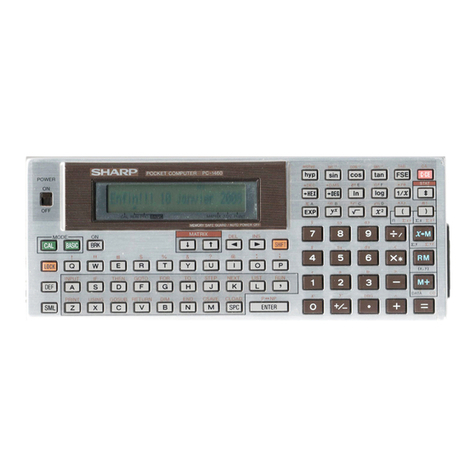
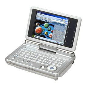
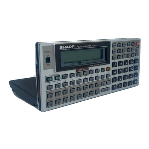
Sharp PC-1600 User manual

SHARP
SERVICE MANUAL
-
PC-l600
CODE:OOZPC1600SMEl
MODEL PC-1600
This manual contents CE·1600P/CE·1600F/
CE·1600M/CE·1600L/CE·1601 L/CE·1602L/
CE·1603L/CE·1609L
__ ----------------------CONTENTS---------------------- __
1. Scope 1
2. Specification . . . . . . . . . . . . . . . . . . . . . . . . . . . . . . . . . . . . . . . . . . . . . . . . . . . . . . . .. 1
3. System configuration 3
4. PC·1600 block diagram 4
5. Memory mapping 7
6. Power supply . . . . . . . . . . . . . . . . . . . . . . . . . . . . . . . . . . . . . . . . . . . . . . . . . . . . . . .. 11
7. System operation 11
8. Service precations . . . . . . . . . . . . . . . . . . . . . . . . . . . . . . . . . . . . . . . . . . . . . . . . . . .. 15
9. LSI pin descriptions 20
10. Connection locations and interface signal identification 35
11. Circuit diagram and P.W.Bparts
&
signal position 39
12. Parts list and parts gued 57
*
CE·1600P 63
*CE·1600F 98
*
CE-1600M 105
*
CE-1600L 110
*
CE-1601L 111
*CE-1602L 112
*
CE-1603 L . . . . . . . . . . . . . . . . . . . . . . . . . . . . . . . . . . . . . . . . . . . . . . . . . . . . . . . . .. 113
*
CE-1604L 114
SHARP CORPORATION

1. Scope
The PC·1600 has been designed with the following versatile
features:
1. The most of PC·1500 BASIC software and the PC·1500
hardware options are compatible with the PC·1600.
2. Advanced technology gives the PC·1600 new features
not available on the PC·1500.
1-1. Compatibility with the PC-1500 BASIC
simulation mode
For compatibility with succeeding models, most of soft-
ware created in BASIC for the PC·1500 can also run on the
PC·1600.
(a) For display in the simulation mode, a single line on the
bottom of the display rows is subject for execution.
(b) In the simulation mode, the same character codes of
the PC·1500 are used.
(c) The PC·1600 must work with a variety of PC·1500
software programs that include an option
control-
ling system, and the PC·1600 system bus signals are
upper grade compatible with the PC·1500 system bus.
(Consideration is given for the use of the CE·150, 158,
and 162E.)
(d) The slot signals are also upper grade compatible; th is
allows the use of the PC·1500 memory module on
-the PC·1600.
2. Specifications
• Model name: PC·1600
• Keyboard layout:
-
PC-1600
(Memory modules usable: CE·151, 155, 159, and 161.)
The CE·150 does not meet the upper grade corn-
patibility test for software that uses the REM·1 because
of a functional restriction on the PC·1600 optional
printer CE·1600P, since the CE-150 has two data
recorder remote control terminals (REM·O and REM·1).
1-2. Implementation of functions that were not
feasible with the PC·1500
(a) Adoption of a 26-digit by 4·line alphanumeric LCD
unit.
(b)
Operation
speed
of the PC·1600 is approx.
2.5
times
faster than that of the PC·1500 as a result of using the
general purpose microprocessor (Z·80) as the main
CPU.
(c) Increased expansion module slot (two slots).
(d)
I
ncreased user memory area (11,834 Bytes user area
out of 16KB basic RAM area},
(e) Implementation of the EIA, conforming to the internal
RS·232C interface for communication.
(fl Implementation of the system
wake-up
(modem phone
and timer started) and alarm functions.
(g) Adoption of the analog input, bar code reader input,
and external keyboard input interface.
(h) Use of the internal optical fiber (SIO) interface.
(1) Alphabetic keys
(2) Small key
(3)
Shift key
(4)
Function keys
(5)
On and Off key
(6) Clear key
(7)
Mode
key
(8) Numeric and Arithmetic Operation keys
(9) Enter key
-1-

1. Scope
The PC·1600 has been designed with the following versatile
features:
1. The most of PC·1500 BASIC software and the PC·1500
hardware options are compatible with the PC·1600,
2. Advanced technology gives the PC·1600 new features
not available on the PC·1500.
1-1. Compatibility with the PC-1500 BASIC
simulation mode
For compatibility with succeeding models, most of soft-
ware created in BASIC for the PC·1500 can also run on the
PC·1600.
(a) For display in the simulation mode, a single line on the
bottom of the display rows is subject for execution.
(b) In the simulation mode, the same character codes of
the PC-1500 are used.
(c) The PC·1600 must work with a variety of PC·1500
software programs that include an option control-
ling system, and the PC·1600 system bus signals are
upper grade compatible with the PC·1500 system bus.
(Consideration is given for the use of the CE·150, 158,
and 162E.)
(d) The slot signals are also upper grade compatible; th is
allows the use of the PC·1500 memory module on
-the PC·1600.
2. Specifications
• Model name: PC·1600
• Keyboard layout:
-
PC-1600
(Memory modules usable: CE·151, 155, 159, and 161.)
The CE·150 does not meet the upper grade corn-
patibility test for software that uses the REM-1 because
of a functional restriction on the PC·1600 optional
printer CE·1600P, since the CE·150 has two data
recorder remote control terminals (REM·O and REM·1).
1-2. Implementation of functions that were not
feasible with the PC·1500
(a) Adoption of a 26-digit by 4·line alphanumeric LCD
unit.
(b) Operation speed of the PC·1600 is approx. 2.5 times
faster than that of the PC·1500 as a result of using the
general purpose microprocessor (Z·80) as the main
CPU.
(c) Increased expansion module slot (two slots).
(d) Increased user memory area (11,834 Bytes user area
out of 16KB basic RAM area),
(e) Implementation of the EIA, conforming to the internal
RS·232C interface for communication.
(fl Implementation of the system wake-up (modem phone
and timer started) and alarm functions.
(g) Adoption of the analog input, bar code reader input,
arid external keyboard input interface.
(h) Use of the internal optical fiber (SIO) interface.
(1) Alphabetic kevs
(2) Small key
(3)
Shift key
(4) Function keys
(5) On and Off key
(6) Clear key
(7) Mode key
(8) Numeric and Arithmetic Operation keys
(9) Enter key
-1-

PC-1600
• Display unit:
FEM-LCD (LF·7204E)
Graphie display: 156 x 32 dots, 16 symbols
Character display: 26 digits
x
4 lines
(4.5) 5.375 5.9 1 1 7 2.55
6.85
8.3 3.95 49.35 3.65 4.3 5.3 4.25 44.5)
J\
»<:
I--"
I----'
r--
'"
....
1.735 0.3 3.25 3.01 0.7 .as.
'"
~
0.6 - t--
er:
0.575 2.675 2.44
1Q1...
2.44 1.5
....
t-
.
-
. .
BUSY SHIFT 1!I(.o-7~:lJ7) SMALL DEGRAD RUNPRO RESERVE DEF I
um
(SATT
I
,
~
-.
'"
156x32
Dots
0
I
'"
5
I
~l~
I
;;>
o
0
~
\1
r=---17
,
==
b:::::.-'
l
v
_j
-
;;;;"
.
-
.
.
~.f.r.nce Wind~ frame
101
x'26 4-R
0.5 '/
-
~I:i
I
Reference line / ~
90.43 11.285~8:~
Note 1 unit: mm
• Calculation capacity:
10 digits (mantissa)
+
2 digits (index)
• Calculation method:
Formula based (with priority discrimination feature)
• Programming language:
BASIC (PC·1500 upper grade compatible)
• Internal system configuration:
Main CPU:
SC7852 (CMOS,
Z·80
compatible, 3.58MHz basic clock]
LH5803 (CMOS, 8·bit microprocessor, 2.6MHz basic
clock)
Sub CPU:
LU57813P (CMOS, 4·bit microprocessor, 307,2KHz
basic clock)
ROM:
96KB (BASIC interpreter) - (80KB for the
Z·80
and
16KB for the LH·5803)
RAM:
16KB (user area: 11,834 bytes), incremental up to
80KB.
• Basic calculation functions:
Basic calculation:
Four rules of math.
Scientific calculation:
Trigonometrie function, inverse trigonometric function,
logarithm, exponential, angular conversion, power raising,
square root, integral, absolute value, signum, circle ratio.
• Edit functions:
Horizontal cursor movement control (..., ~, CTR L
+
character keyI
Insertion (INS), deletion (DEL, CTRL
+
character key)
Une up and down
(i-,
t)
Fig.l
• Interrupts:
Timer interrupt, RS·232C interface interrupt, analog
input interrupt, function key interrupt
• Interfaces:
RS·232C interface, optical SIO interface, analog signal
Input interface
• Other functions:
Weak battery detection, timer function, automatic
power-on (by the internal timerl, power-on from the
telephone line (to the RS·232C interface via the modem
phone), automatic power-off
• Memory protection:
Battery backup (program, data and reserve memory con-
tents are saved upon power-off, and the backup battery
of the AC adaptor in use)
• Operating temperature:
0° to 40°C
• Power supply 6V ... (DC):
SUM·3 x 4 (AA) (x4)
AC adaptor option (EA·160) (accessory of the CE·
1600P optional printer)
• Battery power retention time (AA):
About 25 hours with SUM·3 in use; 10 minutes of
operation or program execution and 50 minutes of data
on display per hour under the operating temperature of
20°C.'
• It may vary depending on the kind of battery and use.
• Power consumption:
0,48W
• Physical dimensions:
195mm (W) x 86mm (0) x 25.5mm (H)
• Weight:
375g (including batteries)
-2-

• Accessories:
Soft case, template (x 1), SUM·3 batteries (AA) (x
4),
instruction manual, BASIC language manual, name
label
3. System configuration
CE·1600P Printer with Cassette Interface
~
Ilenlenll==dl
0
-
\
~/
CE·1600F Floppy Disk Drive
•
[IJ
.
CE·162E Parallel and
Cassette Interface Unit
I
CE·1650F
Floppy Disk
o
CE·158 Serial and
Parallel Interface Unit
\
\
\
\
\
\
\\
\\\\\
SHARPPC-1600
Pocket computer
I Siot 2 ~IOt
1
!
t t
:~~
/ RAM Modules
/ lii2lI
UI'Eii!I!I
I
CE·161 CE-151
I
CE-1600MCE-155
I CE-159
I CE-161
-
PC-1600
\
\
\
\
\
\\
\
\
\
\
\
\
\
\
\
\
\
\
CE-1600L
Optical Optical
Serial Port Fiber Cable
==,,__.o--c:>
Analog
Input Port
- ---- 8
RS·232C
I
Serial Port
,
,
I
,
,
:I,
CE-152
J
CassetteRecorder
16L
__Die
CE·1601L
Cable
CE-1602L
Cable
CE·1603L
Cable
CE-1604L
Cable
CE·150 Printer with Cassette Interface
NOTE: The PC-1600 option (CE·1600P) cannot be used
in conjunction with the PC·1500 option (CE·150,
CE·158, CE·162),
CE·515P Printer I
r.
CE.516PPrinter
o!-'-ilJ
Aco~stic
Coupler
I
r.
or Olrect Modem
o!-'-ilJ
MZ-5500, MZ-5600
I
rv
Personal Computers
c-!-'-a:J
PC-5000Portable Comp-uterl
rv
CE-158Serialand I~
Parallel Interface Unit
PC·7000 Personal Computer
I
oD-liJ
IBM PersonalComputer
-<:1-

-
PC-1600
4.
PC-1600
bloc~
diagram
5
Y
5
T
E
M
HD61203 (5))
LCD LCD
r-
C. DRIVER
HD61102 HD61102 LH·5803
~
LLCD 5. DRIVE LCD 5. DRIVE
~
MAIN CPU
2
5C78!i
..._
LR38041
IGATE ARRA1 32KB ROM ~ l8KB R~~
......
MAIN CPU
r--
x3
1
I--
..._
TC8576F LU57813P
r--
ON
J
UART I
J
5UB·CPU RE5ET
-,
I
t--
.___
ON
I
KEYBOARD
r--
BX7269W
J
CONVERT
I
ANALOG IN
.__
2
B
U
5
5
L
o
T
1
5
L
o
T
2
5
I
o
R
5
I
2
3
2
C
3.58MHz
Z·80 BU5
..... ....
"I r
CGC
!
L
Z·80 LH
I/F
J----1.~
II
1
LH·5810 Interrupt Memory
1/0
control
compatible control control
JJ
1
-r
~
L...O
MAIN CPU 2
LH·5803
Keyboard
Buzzer
Cassette
Timer
R5232C
5ystem bus
UART
Main unit RAM
5LOTl
SLOT2
Main unit ROM
etc,
Main CPU internal block diagram
Fig.2
-11.-

4-1. Relation of the main CPU-1 to the main
CPU·2
Since two CPUs are linked together, the bus line of one
CPU is on the sytem bus; the other CPU bus is kept in the
floating state.
Shown in the following table are the bus signals of the two
CPUs in connection.
SC7852 signal name Z-80 signal name LH·5803 signal name
A15 - AO A15 - AO A15 - AO
OS7 - OBO 07 - 00 07 - 00
MREQ Opposite polarity MEO
of MREQ
10RQ Opposite polarity ME1
of IORQ
RO RO 00*
WR WR R!W
*The
00
output of the LH·5803 is connected to
RD
of
the SC7852 via the gate array (LR38041).
The operating CPU is indicated by the ELH signal.
ELH
=
Low: LH·5803
ELH
=
High: Z·80
Z-80 LH·5803
LH-5803 Z-80
RSTO
LHWAIT
___ --;... _J
Z·BO
instruction
HALT
OUT(38H)A
LH·5B03
instruction
HALT
OUT(38H), A
STA #A03BH, A
Fig.3
The following takes place when areset is applied to the
SC7852 (RSTIN
=
Low).
CD
ELH goes to high to indicate that the Z·80 is in
operation. At the same time, areset is applied to the
LH·5803. This allows the Z·80 to operate after the
completion of the reset.
@With the following instruction, the Z·80 hands down
the control to the LH·5803.
OUT(38Hl, A .... Ais don't care.
HALT
After the execution of the above instruction, the Z-80
bus is set in the floating state. At the same time, ELH
goes to low along with RSTO, and the reset is cleared
to the LH·5803 to start its operation.
®With the following instruction, the LH·5803 hands
down the control to the Z·80.
STA #A038H
A wait is applied to the LH·5803 (LHWAIT=High) to
stop the operation of the LH-5803. When ELH goes to
high, the LH·5803 bus is set in the floating state, With
this, the Z·80 starts to operate.
CD
In order that the Z·80 may hand down the control to
the LH·5803, the Z·80 stops after the operation as in
step 2 and the Z·80 bus is set in the floating state.
-!')-
-
PC-1600
Then, ELH goes to a low level so that the LH·5803 bus
is activated. LHWAIT now goes to low which causes
the LH·5803 to operate.
4-2. Sub CPU role
The sub CPU has the following roles.
(1) Main power-on and main power-oft
CD
When the svstern-off command is received from the
main CPU, the system is turned off.
@The system is turned on when the system is switched
on by the ION Ikey.
(21 Real timer
CD
Similar to the PC·1500; month, day, hours, minutes,
and seconds are controlled by the PC·1600, though a
leap year is not issued.
@A single wake-up timer and two alarm timers (in-
cremented at every 0.5 second) are controlled.
(3) Weak battery detection
A weak battery condition is monitored by the A/D
converter function held by the sub CPU.
CD
The level of the PC·1600 main power supply ischecked.
@Also, the level of the power supply to the PC-1600
option is checked.
When it drops below the given level, the symboilBATTI
is activated on the LCD, When the hardware-monitored
weak battery signal is turned to high, the system is
then turned off.
(4) Analog input
The level of the input signal received through the
PC·1600 analog input jack is A/D converted and
returned to the main CPU.
Also, an external keyboard input through the same
jack may be read and returned to the main CPU.
(5) Click sound
A click sound feature is supported by the PC·1600.
When a keyboard entry is sensed in the click generate
mode, the command is issued from the main CPU to
generate a click sound.
(6) Reset signal
Two reset signal input lines are supported. When a
signal is received on either line, areset is applied to the
system for the prescribed time (30 milliseconds).
CD
RESET switch on the back of the PC·1600
@RESET switch on the back of the CE·1600P
(7) System-on function with the CI signal of the RS·232C
interface (checked at every 0.5 second)
(8) Timer signal outout (1/64 sec.)
4-1. Relation of the main CPU-1 to the main
CPU·2
Since two CPUs are linked together, the bus line of one
CPU is on the sytem bus; the other CPU bus is
kept
in the
floating state.
Shown in the following table are the bus signals of the two
CPUs in connection.
SC7852 signal name Z-80 signal name LH-5803 signal name
I
A15 - AO A15 - AO A15 - AO
OB7 - OBO 07 - 00 07 - 00
MREG Opposite polarity MEO
of MREG
10RG Opposite polarity ME1
of IORG
RO RO 00*
WR WR R/W
*The
00
outpur
of the LH·5803 is connected to
RD
of
the SC7852 via the gate array (LR38041).
The operating CPU is indicated by the ELH signal.
ELH =Low: LH·5803
ELH
=
High: Z·80
RSTIN
ELH
RSTO
LH·5B03
LH·5803 Z-80
Z·80
LHWAIT
---+---____j
Z·80
instruction
HA LT
OUT(38H)A
LH·5803
instruction
HALT
OUT(38H), A
STA #A038H. A
Fig.3
The following takes place when areset is applied to the
SC7852 (RSTIN
=
l.ow).
CD
ELH goes to high to indicate that the Z-80 is in
operation. At the same time, areset is applied to the
LH-5803. This allows the Z-80 to operate after the
completion of the reset.
®With the followinq instruction, the Z·80 hands down
the control to the LH-5803.
OUT(38Hl, A .... Ais don't care.
HALT
After the execution of the above instruction, the Z-80
bus is set in the floating state. At the same time, ELH
goes to low along with RSTO, and the reset is cleared
to the LH-5803 to start its operation.
®With the following instruction, the LH-5803 hands
down the control to the Z-80.
STA #A038H
A wait is applied to the LH-5803 (LHWAIT=High) to
stop the operation of the LH-5803. When ELH goes to
high, the LH·5803 bus is set in the floating state, With
this, the Z·80 starts to operate.
CD
In order that the Z-80 may hand down the control to
the LH·5803, the Z-80 stops after the operation as in
step 2 and the Z-80 bus is set in the floating state.
-!)-
-
PC-1600
Then, ELH goes to a low level so that the LH-5803 bus
is activated. LHWAIT now goes to low which causes
the LH-5803 to operate.
4-2. Sub CPU role
The sub CPU has the following roles.
(1) Main power-on and main power-off
CD
When the system-off command is received from the
main CPU, the system is turned off.
®The system is turned on when the system is switched
on by the
ION I
key.
(2) Real timer
CD
Similar to the PC-1500; month, day, hours, minutes,
and seconds are controlled by the PC-1600, though a
leap year is not issued.
®A single wake-up timer and two alarm timers (in-
cremented at every 0.5 second) are controlled.
(3)
Weak battery detection
A weak battery condition is monitored by the A/D
converter function held by the sub CPU.
CD
The level of the PC·1600 main power supply ischecked.
®Also, the level of the power supply to the PC-1600
option
is checked.
When it drops below the given level, the symbol!SATT!
is activated on the LCD. When the hardware-monitored
weak battery signal is turned to high, the system is
then turned off.
(4)
Analog
input
The level of the input signal received through the
PC-1600 analog input jack is A/D converted and
returned to the main CPU.
Also, an external keyboard input through the same
jack may be read and returned to the main CPU.
(5) Click sound
A click sound feature is supported by the PC-1600.
When a keyboard entry is sensed in the dick generate
mode, the command is issued from the main CPU to
generate a click sound.
(6) Reset signal
Two reset signal Input
tines
are supported. When a
signal is received on either line, areset is applied to the
system for the prescribed time (30 milliseconds).
CD
RESET switch on the back of the PC-1600
®RESET switch on the back of the CE·1600P
(7) System-on function with the CI signal of the RS-232C
interface (checked at every 0.5 second)
(8) Timer signal outout (1/64 sec.)
-
PC-1600
4·3. Sub CPU operation
(Interfacing with the main CPU)
TC8576F (UART) LU57813P (sub CPU)
D7-
(data
DSTB KI
BUSY ZlD
ACK Z9
DATAS Rl3~ROO
DATAl
r-----------,
I
,
II
I
,
,
,
)0
_.
,
Buffer
....
'
R33~R20
bus)
<
,
-
,
,
I
I
,
,
,
f
I
,
-_.-
,
10RP
(from SC7852)
,
~------r---~
Contained in the LR38041 gate array
Fig.4
Signals interfaced with the main CPU are KI, Z10,
Z9,
R13~ROO, and R33~R20.
RI3-ROO=:>( Command
X'- _
KI ~
Z10
~ ..... 'B~;;"
---r
=fJt
'9.5
µ,
ReadyReady
Z9
R33-R20
X
10RP
Return data
The following shows signal timings.
Send command
---------, I
I
I
Read return data
-~-
CD
Before the Z·80 CPU sends a command to the sub
CPU, the sub CPU is asked if it is ready to receive the
command. If it is not, the Z·80 waits until the sub
CPU becomes ready.
The Z·80 assumes the sub CPU to be ready if the
BUSY input of the UART is high.
®Next, 8·bit command data are sent to the sub CPU.
The Z·80 sends the da ta on the DA TAl ~DA TA8 port
of the UART, wh ich are received by the sub CPU
through R13~ROO. Unless ACK is returned within one
second, the Z·80 proceeds to the next processing.
®The Z·80 sends a pulse signal on DST8 of the UART in
order to inform the sub CPU a command request,
which the sub CPU receives of through the Klline.
With the KI line of the sub CPU high, an interrupt
is se nt to the sub CPU, and the command is processed
in the interrupt service routine.
G) One of the following requests may be made depending
on the command issued from the Z·80.
(i) Arequest for return data
(ii) Arequest not to return data
The sub CPU then interprets the above to proceed to
the next
step,
(i
I
A pulse signal is sent on Z9 after sending the
return data on R33~R20, to indicate completion
of the command execution.
(ii)
A pulse signal is sent on Z9 to indicate receipt
of the command.
In either case, the Z·80 waits for a high pulse signal
state on
Z9.
The high state received on Z9 is then input to the
ACK line of the UART and latched internallv, The
Z·80 checks the latch if it is okay.
®When the Z·80 accesses 33H of 1/0 to request the
return data, it forces 10RP to low so that the LR38041
gate array internal buffer is opened to send the return
data (R33~R20) on the Z·80 bus D7~DO.

5. Memory mapping
5-1. Memory map asseenfrom the Z·80 (SC7852)
OOOOH
4000H
8000H
COOOH
FFFFH
-
PC-1600
PC·1600
ROM
(CSOO1)
I
PC·1600 PC·1600 CE·1600P CE-1600P
Siot 2 ROM ROM ROM
S2
I
(Printer) (Floppy
ROM (C) (CS24) disk)
(CS001 )
I
Cassette
I
PC·1600
Siot 1 Siot 1 Siot 2 Siot 2
S1 Sl S2 S2
(A) (B) (C)
(0)
ROM
(CS24) (CS123)
PC·1600
(RAM3)
-_.-
Bank 0 Bank 1 Bank 2 Bank 3 Bank4 Bank 7
The memory space directly accessible by the Z·80 is 64KB,
however, the memory space is expanded to 320KB for the
PC·1600 by means of bank selection. Bank selection is done
according to the contents of the Z·80 I/F address 31 H.
When the Z·80 accesses aspace in 000H~3FFFH, bank
o
or bank 1 is selected depending on the status in bit
o
(bO) of the
1/0
address 31 H.
If bO =0, bank 0
-+
PVOUT: 0
If bO =1, bank 1
-+
PVOUT: 1
PVOUT (SC7852 output) is used to represent the chosen
bank (0 or 1). PVOUT is 0 when bank 0 is selected. It is
1 when bank 1 is selected.
Similarly, when the Z·80 accesses aspace in 4000H ~
7FFFH, bank 0 ~ bank 7 is selected depending on the
status in the bits, b3 ~ bl. PVOUT, PU, and PT are used
to represent bank 0 thru bank 7.
The PVOUT, PU, and PT conform to the
1/0
address 31 H
and the space accessed
by
the Z·80.
It is possible to sense the status of the
1/0
address 31 H,
Bank 5 Bank 6
Table·2
Bank
z·ao
accessing Status in the 1/0
PT PU PV
No.
space address31H
OUT
b7 b6 b5 b4 b3 b2 bl bC
0
OOOOH-3FFFH
·
·
· ·
···
·
.
.
0
1
t
·
*
····
*
1
.
*
1
0
4000H-7FFFH
* * * *
0
00
*
0
0 0
1
t
*
· ·
·
0 0
1
·
0
0
1
I
2
t
· ·
· ·
0
1
0
·
0
1
0
3
t
·
*
·
*
0
1 1
*
0
1 1
C
t
· ·
· ·
1
00
·
1
0 0
5
t
·
···
1
0
1
·
1
0
1
6
t
·
·
· ·
11
0
·
1 1
0
7
t
·
· · ·
1 1
1
·
1
1 1
08000H-BFFFH
·
0
0
0
·
···
0
0
0
1
t
·
0 0
1
·
· ·
·
0 0
1
2
t
·
0
1
0
· · ·
·
0
1
0
3
t
·
0
1 1
·
* * *
0
1
1
C
t
·
1
00
* *
·
*
1
00
5
t
*
1
0
1
***
*
1
0
1
6
t
*
1
1
0
* *
*
*
1
1
0
7
t
·
1
1
1
·
* *
*
1
1
0
0COOOH-FFFFH 0
*
·
*
*
·
*
·
*
.
0
1
t
1
* * * *
*
·
*
* *
1
': DON'T CARE

-
PC-1600
5-2. Chip select signal
(1) CSOOl
This signal must be low to accessthe memory space in
0000H-7FFFH of bank O. The signal is also an input
to the CS line of the ROM.
(2) CS123
This signal must be low to access the memory space
of 8000H-BFFFH of bank 6. The remaining 16KB
area of the second half is for the LH·5803 control
ROM. This signal is also an Input to the CS line of
the ROM.
The ROM (64KB) selected by CSOOl or CS123 is
cleared when a high signal is given to the INH line
which is connected to the system bus and slot (pulied
down to low within the main unit).
(3) CS24
This signal must be low to accessany one of the 16KB
spaces.
(a) For accessing of bank 3 of the memory space in
4000H -7FFFH.
• CS24 is an input to the CS line of 256K bits
ROM.
• A15 is connected to OE of the ROM.
• This 16KB space is further banked by another
port signal to compose a 32 KB area.
(4) RAM3
This signal must be high to accessthe memory space
in COOOH-FFFFH of bank O. This signal is connected
to CE2 of the two 8KB RAMs. A13 is used to
determine wh ich RAM is to be selected.
OOOOH
5-3. Memory map as seen from the LH-5803
4000H
8000H
COOOH
FFFFH
8KB RAM CEl input Memory spacechosen
A13 COOOH~DFFFH
A13A (inverted A13 gate array output) EOOOH~FFFFH
(5) RAM2
Memory select signal for the memory slot 1 (Sl).
This signal must be low to accessthe memory space in
8000H-BFFFH of either bank 0 or bank 1.
1.
(6) RAMl
Memory select signal for the memory slot 2 (S2).
This signal must be low to access the memory space
in 8000H-BF FFH of either bank 2 or bank 3.
It is possible by means of software to copy 16KB
of memory space in 8000H-BFFFH onto 16KB
of memory space in 4000H-7FFFH of bank 1. (This
area is reserved for the application module which is
expected to be made availabel soon,)
Sl Sl S2 S2
RAM2 RAM2 RAMl RAMl CS24
RAM
16KB
RAM3
-------
-------
CE·150 CE·158
PVOUT= 0 PVOUT=1
ROM
16KB
(CS123)
Bank
0
Bank 2 Bank
7
Sank 1 Sank 3 Bank 4 Bank 5 Bank 6
o

(1) The memory space in OOOOH"'3FFFH is the same as
the memory space in 8000H"'BFFFH of the Z·80. The
method of accessing is also the same.
(2) The memory space in 8000H"'FFFFH is the same as
that in the PC·1500. The PV signal of the LH·5803
is used to select the bank for 8000H"'BFFFH. (The
PV signal of the LH·5803
is
directly sent by PVOUT
of the SC7852.)
5-4.
1/0
mapping
The
1/0
space of the Z·80 consists of 256 bytes in OOH'"
FFH.
OOH Useprohibited.
OFH
lOH Port corresponding to LH·5810 (LH·581l) contained
1FH in the SC7852 (not synchronized with
<pOS).
20H TC8576F UART selection
27H
28H S2 (slot 2)
2FH
30H SC7852 internal LSI control register port
3FH
40H System reserve
I
4FH
50H HD61202 (IC2). (IC3)
58H HD61202 (lC3)
-
--
5BH HD61202 (lC2)
System reserve
60H S2 (slot 2)
6FH
78H CE·1600F
7FH
80H CE·1600P
83H
84H
F8H
\
\
_0_
-
PC-l600
\\
\
\
\
\
Z-80
1/0
LH·5803 Read Write
address address
30H #A030H 10R MOD 10WMOD
31H #A031H 10R MAP 10WMAP
32H #A032H 10R INT 10WPRI
33H #A033H IOR P 10WCDF
34H #A034H 10R LHMSK 10W LHMSK
35H #A035H 10R ZMSK 10WZMSK
36H #A036H 10R ADRS 10WCLl
37H #A037H 10R KB 10WCGC
CGC register wrlte
38H #A038H
~
10W STP
39H #A039H
~
10WVCT
3AH #A03AH
_.::::-:::::_
10W KA Not used
3BH #A03BH
~
10W KS Not used
3CH #A03CH
~
10WSLT
3DH #A03DH
~
10W
C/D
3EH #A03EH
~
-
-
\
-
I
3FH #A03FH
-
-
-
-
-
-
NOTES:
#
(Rreg): Indicates the contents of the memory
(MEl
accessed) which are implied by the LH-5803
CPU internal register (R register).
r==J:
Vacancy in the Z·80
1/0
map wh ich is not used
at present.

-
PC-1600
6. Power supply
6-1. Kinds of power supplies
Power Voltage Oescription
~
supply range
!
VGG 4.0 ~ 4.7V • Logic driving power which is on while
I
the system is not operating. Power is
i
supplied to the chips that need protec-
tion.
(1) RAM16KB
Memory protectlon
(2) LU57813P
Real-time timer and wake-up timer
protection
(3) H061102
Display data protection which is
required to activate the display at
power-on after auto power-off.
(4) LR38041
To maintain the signal level of such as
the memory select signal at a non-
active level.
VCC 4.0 - 4.7V • Logic driving power which is shut off
when the system isturned off. Power is
supplied to the chips that do not need
protection when the system is off.
(1)ROM
256Kbit
(2)CPU
SC7852, LH5803
(3) H061203(S)
LCD common driver chip
(4) TC8576F
UART LSI
VEE Approx. • For creation of a low voltage to the
-8.5V LCO drive voltage and the RS·232C
interface signals.
VOD Approx • For creation of a high voltage to the
6.0V RS-232C interface signals. This voltage,
however, is supplied when PRIME is at
a high level (RS·232C is chosen) and
shut off when PRIME is a low level.
6-2. Power generation method
The following power supply sources are used to generate
the above power requirements.
(1) Internal dry battery cells (x
4)
(2) Through the AC adaptor
(3) Supplied through the VBAT of the system bus
A high voltage supply level is used by the PC-1600.
(i) VGG
A
voltage of
about 4.7V
is normally supplied
from the above source. The voltage drops when
the level of power supply decreases.
(iil VCC
VGG is supplied through this line, when BFO is at
a low level or ACL is at a high level.
VCC is not supplied when the system is off.
(iii) VEE
VEE is supplied when the system is turned on.
(iv) VDD
VDD is supplied when the PRIME output is at a
high level with the system on.
6-3. System-on/system-off
The on/off state of the system is controlled by the LU
57813P. The on/off state of the system is seen on the
BFO output. When BFO is low, the system is on and
VCC and VEE are available. When the system is off, no
power is supplied except VGG.
(1) System-off to system-on
There are five ways.
(i) Use of the BREAK/ON key
(ii) By means of the wake-up function
Possible to disable with mask
(iii) By means of the RS·232C interfacing CI signal
(iv) Use of the ALL RESET switch (ACL signal)
located on the back of the PC-1600
(v) By means of the reset input from the CE-1600P
Normally, the svstern is turned off with (i).
(21 System-on to system-off
There are two ways.
(i) By means of the Z-80 command
(ii) By means of the weak battery detect signal (03)
7. System operation
7-1. System-off operation
LSls operated by VGG, except for the LU57813P, are
assigned to protect their contents.
For the LU57813P, the real timer needs to be revised when
the system is off. So, an interrupt is sent to the LU57813P
by the internal timer every 0.5 second
to
revise the real
timer. When seconds are carried to aminute, the time is
verified with the wake-up timer and the alarm time. There-
fore, a system
clock
(153.6KHz or 307.2 KHz) is issued on
FOUT of the LU57813P every 0.5 second,
The system starts to rise when 01 of the CI connected
subcontroller remains high for more than the predeter-
mined time; the system wake-up is also possible by the CI
input
of
the RS-232C interface which is input at 0.5
second intervals.
But, if the system is forced off because of a weak battery
condition (03 input at high), the 0.5 second interval timer
interrupt is not activated even if the weak battery
con-
dition is cleared.
11\

1\
System-off (down) in the Normal system-off
Q3 state
1The real-time timer is not A timer interrupt is issued
revised. every 0.5 second to revisethe
real-time timer.
2FOUT is not issued. FOUT is issuedevery 0.5
second.
3
The
svstern
can
be
turned The
svstern
can be turned on
on by one of the following by one of the following
operations after clearing the operations.
weak battery condition.
CD
Depressionof the
CD
Depressionof the SREAK/ON key
BREAK/ON key
®
Depression of the ALL
®
Depressionof the ALL RESET SWITCH located on
RESET switch located the back of the PC·1600
on the back of the
®
Depressionof the RESET
PC·1600 switch located on the back
of the CE·1600P
G)
When the wake-up time
meets the real time as
programmed by the
WAKE$(O) statement
®
When the R5-232C Interface
CI input is set high by the
WAKE$(1) statement
The figure below shows the timings when the system turns
off.
VCC
VEE
..J
PRI:~ ~~~~--~-~~~~
~~~~~i~~~-_-_-_-_-_-_-~~~~~~~~~~~~~~~~~~~~~~~
P3
=
BFO
P2 =
SLcT
P1 •
SLcB
po-
ASTIN
Z15 -
zoo
A33 - A::20:...___
__l _
lIUU1nIUl _
Il_fl 00 _
cLK· 3.58MHz
CKO
=
217KHz
CD
When the subcontroller receives the system-off corn-
mand from the main CPU, it confirms that both
00 and KH are at a low level, Then, P2 and SLCT
are forced to low to disable the memory selection. If
KH is at high, the control proceeds to the system in
sequence.
®Then, P3 and BFO are set to high to turn off the
system power supptv, Wlth this, all
lnputs
and outputs
of the SC7852 and LH·5803 are turned to a low or
high impedance.
®The subcontroller goes into the standby mode, but
the real-timer issues a timer interrupt ever 0.5 second.
second.
(a) If the wake-up timer has been set, the time on
the real-timer is checked for whether it coincides
-11-
-
PC-1600
with the wakeup time. If it coincides, the system
is turned on.
(b) If the wake-up timer is set to turn on the system
with the RS-232C interface CI Input, the system
is turned on with the input of the CI signal as it
has been monitored.
If the weak battery signal Q3 goes high when the
system is off, the system down is established.
7-2. System-on operation
The figure below shows the timing sequence when the
system is turned on by the BREAK/ON key.
vcc
======;-_J
;-----------------------
B~(ON) ~
Z13
L__
KH ""' 30m2::==:j
PO=RSTIN ,
P3
=
BFO
P1
= SLCB
-1
P2=SLCT ~ ~~~
Z15"" ASTE ." Peripheral reset ~'l:-,-~:_1_m_' _
A
"
BREAK Key
!l:iID
entry
t
System- Z-80
reset clear
on
Z12 ~ ~
A
Prohibit sending KCI
input
to
B5R
01
T8576F
PRIME
510 interface ,elected
-----------------
, "n"_
CLK
=
.:'~~8_":'I~~ :__
JU U:
MREQ :
-------------------:-------
,
,/1
: Z-80
starts
-
ELH
00 _
RSTO
CD
When the BREAK/ON key is pushed while the system
is off, the ON input of the LR38041 converts to low.
As Z13 is low, KH goes high.
®When KH goes high, the subcontroller starts to operate
assuming the start of the system. First, P3 is set low,
P2 low, Pl high, and PO low. Now, VCC is activated
because P3 and BFO are low, and the system reset
is applied with low PO and RSTIN states. The memory
and
1/0
selections are prohibited in low P2 and SLCT
states.
®Low PO and RSTIN states are issued for 30 milli-
seconds.
G) The Z15 peripheral reset output is issued for 1 mil-
lisecond to reset peripherals.
®First, P2 and SLCT are set to high to select memory
and
1/0,
then the system reset is cleared.
®In order to supply stable docking to the Z·80, it takes
about 0.3 millisecond before supplying the system
clock ,

PC-1600
CD
After the system reset has been cleared, the Z-80 starts
operation within 10 microseconds and the Z-80 begins
to read the contents of the address OOOOH.(MREQ
issued)
®Now, the Z-80 starts to supply cloek pulse to the
HD61203 LCD driver (217KHz on the CKO) to
activate the LCD.
• The LCD voltage VEE is activated at the same time
the system is turned on.
• Supply voltage VDO on the RS·232C high level side
will be issued only when PRIM is at a high state.
But, VOD is not supplied during power-on because
PRIM is at a low level then.
• A high ELH state indicates that the Z-80 is started
at the time of system reset. The LH-5803 stays
reset (RSTO;High).
7-3. Reset operation
7-3-1. Reset by the ALL RESET switch on the back of the
PC-1600
When the ALL RESET switch is pressed, it causes the
subcontroller Input ACL to go high. With this, the sub-
controller takes the following action by means of the
hardware.
(1) All input and outpur lines, including P3 ~ PO, are
set in the Input mode.
PI
=
SLCB
PO
=
RSTIN
RESETSW
ACL-50347C
ACL·LU57BI3P
__..:,P3 .....,PO ~ The same state as system-on
In the input mode
(80 microseconds)
CD
Regardless whether the system is turned on or off,
P3~PO are set in the input mode and are kept in the
floating condition while the reset is applied to the
subcontroller.
P3 is pulled up with the resistor.
P2 is pulled down with the resistor.
Pl is pulled up with the resistor.
PO is pulled down with the resistor.
While P2~PO are pulled down towards the non-actlve
direction, P3 is pulled up towards the system-off. So,
the system's power supply is turned off in those states.
However, the power is supplied to the svstorn while the
RESET switch is in depression.
7-3-2. Reset by the RESET switch on the back of the
CE-1600P
When the RESET switch on the back of the CE-1600P
is pressed, KL and Z15 of the subcontroller go high. When
this pulse width continues for more than 300 micro-
seconds, the subcontroller proceeds in the same way as
the system power-on procedure so that areset is applied
to the system.
7-3-3. Difference from ALL RESET
The subcontroller interrogates the s'tate of the BREAK/ON
key at 7-3-1 and 7-3·2 above in the following manner.
(1) If the BREAK/ON key is depressed, the all reset is
assumed and all internals are intialized.
(2) If the BREAK/ON key is not depressed, the reset is
assumed - the procedure to turn the system on from
the system-off state. The internals are not initialized
in this case.
It is possible to return reset from all reset by arequest
from the main CPU, the Z-80 asks the subcontroller
for the cause when the reset is applied. Processing
differs depending on the cause.
In the case of all reset ... Clears all memory contents.
In the case of reset ... Retains all memory contents.
7-4. LCD block
7-4-1. General
The LCD is 1/64 duty and consists of 156 x 32 dots and
has 16 symbols.
Y64 (IC3)
Xl-X32
Yl-Y64 (IC3)
(IV)
X49-X64
(11)
(1111
(I)
X33-X64
Yl-Y64 Yl-Y28
Yl-Y64 (IC2)
The 32 vertical dots comprise the following:
(1) Xl~X32 of the IC2 LCD driver outputs take care of
64 dots from the left.
(2) Xl~X32 of the IC3 LCD driver outputs take care of
65~128 dots.
(3) X33"'X64 of the IC2 LCD driver outputs take care of
129~156 dots in conjunction with Yl ~Y28.
(4) X49~X64 take care of 16 symbol dots in conjunction
with IC3 Y64.
7-4-2. Operation
(1) The LCD driving basic clock (217KHz) supplied from
CKO of the SC7852 is connected to the LCD common
driver. Without this signal, the LCD will burn out when
a DC voltage is applied to the LCD.
This signal is issued only during the system-on time
which appears immediately after the clearing of the
reset. As it is in a low state during the reset, a DC
voltage is added to the LCO during that period.
-12-

(2) The HD61202 LCD driver is for the 6800 series; the
timing clock E required for this interface is sent from
the SC7852.
The clock E goes high when the Z-80 accesses 40H-
5FH of
1/0,
(lt has a half clock delay against
10RQ
and its pulse width is 540 nanoseconds.)
But, the HD61102 will not be selected unless all three
chip select lines (CS1, CS2, CS3) are enabled. Two
HD61102s have the following address inputs as shown
in the next table.
-----
HD61102 (lC2) HD61102 (IC3)
CS1 A2 A3
CS2 A5 A5
CS3 A4 A4
Selected
1/0
space 50H - 53H 50H - 53H
58H - 5BH 54H - 57H
(3) For the LCD drive voltage, VCC-VEE are divided by
a resistor to obtain the LCD drive voltages, Vl-V6
and VEE.
VEE is derived from the power supply hybrid IC
50347C.
Vcc
(4~4. 7V) R 1
VI
(HD61203(S), HD61102)
V6
(HD61203 )
V3
(HD61l02 )
V5
(HD61203 )
V4
(HD61102 )
V2
(HD61203(S), HD61102)
R2
R3
R4
R5
VR
VEE VEE (HD61203(S),HD61102'
(=
-8.5V)
7-5. Keyboard block
7-5-1. Key scan timings
Keyboard key scan is done by a Z-80 interrupt with a 1/64
second timer interrupt (subcontroller output INT4).
7-5-2. Method of scanning
Nine key
strebe
signals are obtarneo through
PA7-PAO
anu
PB6 of the SC7852
1/0
port.
Key scan is done in the following ways:
CD
Only the strobe signal of the Y row to be scanned is set
low with other strobe signals set for the input mode.
®
To scan another strobe row after the current strobing
row, a high signal is issued to that strobing row first,
-13-
-
PC-l600
then set in the input mode. So, a low signal is issued to
PA7 - PAO and PB6 at every 1/64 second to discri-
minate a key depression. In this instance, a low signal
is sent to all strobe lines to sense a key depression.
When a key depression is sensed, that particular key is
distinguished after sending astrobe to each line.
As the key input appears on KIN7-KINO of the
SC7852, a row of the keys in a low state is judged to be
the row at which the key entry occurred. Since input
not having a key entry is internally pulled up in the
LSI, it is in a high level.
7-6. Buzzer block
7-6-1. General
These two lines activate the buzzer.
• PC6 output of the SC7852
• Subcontroller F output
7-6-2. Description
As the buzzer is sandwiched between two lines, oscillation
from either line causes the buzzer to activate. Consumption
current is 3 mA, maximum.
(Conditions: Input voltage
=
4.5Vp-p square wave, input
frequency
=
4.1 KHz)
PC6-@-F
(1) PC6
The following three signal sources are connected to this
line.
CD
PB2 Cassette playback signal
®PC7 Cassette recording signal and beep by a
BEEP statement
®SDO ..... Recording signal by the CE-150 or CE-
162E
But, when the beep is turned off, sound is not
generated no matter what the above signals may be.
The above three signallines are normally high.
(2) F
The following three signal sources are connected to this
line.
Ci)
Click .... In the dick mode, a dick is generated
each time a key is pushed.
®Sound generated upon wake-up,
®
Sound generated before issuing an alarm message.
Norrnallv , these three lines are low.
7-7. RS-232C interface and SIO interface
The following serial interfaces are provided for the PC-
1600.
(1) RS-232C
Interface
(COM 1:)
(2) SIO interface (COM2:)
It incorporates the UART TC8576T as the hardware.
While the PC·1600 has two interfaces with single supported
channel, only one interface can be active at one time. The
OPEN or SETDEV statement is used to selectively activate
the channel and the PR IME signal is used to activate the
hardware.

PC-1600
UART
R S·232C interface
Receive
data
At the same time the RS-232C interface is selected with a
high PRIME state, VDD is supplied from the high side of
the RS-232C interface.
The SIO interface is selected with a low PRIME state and
VDD is turned off. During the system on and reset, PRIME
is at low.
PRIME
------------------~
SOF (0_!_jIJJJJJ[j
~====--------------------------
ROF (I)
murrrn
~~L_ __
TXO (0) -- -- --- - -- - - -- -
_n_,
rm:rr:rnn
RX 0
(I)
n -- - -- - - -- -- - -- - -- -,
rrnmunLU..Ll.ll.U.L___
-;:::=========
RTS (0)
CTS(I)
CO
(I)
OSR
(I)
Cf
(I)
OTR (0)
v
00 - - - - - - - - - - - - - - - - - - - - -
TXO(UAR~
ummrn
RXO (UARTJ
UIIIIIIII lIIIIIllIII
CD
When PR IME is at a low state, the RS-232C interface
outputs
either in a high impedance or a low
state
(non-
active).
®When PRIME is at a low state, the SIO interface
1/0
signals, SDF and RDF, are in an opposite polarity with
the UART
Input/output
signals, TXD and RXD. The
start bit is high and the stop bit is low. So, both are
in a low state when no data are sent or received (UART
TXD and RXD are at a high level).
®When PRIME is at a high state, both SDF and RDF are
at a low level and non-active (stop bit}.
@ When PRIME is at a high state, TXD and RXD of the
RS-232C interface are opposite in their
polaritv
as are
those of TXD and RXD of the UART.
@When PRIME goes high, VDD is activated (RS-232C
interface high side voltage),
®The RS·232C interface
input/output
signals-CTS,
DSR, CD, and CI-are
Input
to the UART (opposite
polarity), regardless of the state of PRIME (high or
low),
7-7-1. RS·232C interface signal
Although signals of this interface conform to the EIA
standards, they are used for controls that differ in some
ways from the RS-232C interface in general.
-14-
(1) Input signals are received by the transistor and are
output
through the open collector and pulled up
to VCC using a resistor, as shown in the hybrid
IC BX7269W. A diode is inserted across the base and
emitter of the input which will bring the signal below
the GND level (stop
bit,
etc.) and make it assume to
be at the GND level. Therefore, the input signal is
converted in the hybrid IC to be handled as a logic
signal.
GND
0 I
__jU - __ Vcc
~-GND
-
(2) On the other hand, the
output
signal is
output
through the circuit shown below (hybrid IC),
While the input level is CMOS compatible (0-4.7V),
the
output
is converted to the VDD-VEE level.
The figure below illustrates this.
Va
Vcc
GND
Vb
VDD_j\
Vcc
00-
::: : :::-c- __:-~:-~-=~~-::-~--~-~-~------~--~-~-V
y,""
nnn
Vc
::l I
VEE
CD
When the input (a) is low (GND), the level (b) is below
GND and is assumed by the MN4584 to be at a low
level.
The MN4584 IC is a Schmitt inverter to which VDD
and VEE is supplied. This IC has a hvsteresis against
input.
Output
VEE VTHL GND VnlH VDD Input

In order to change from high to low, the input must
be above VTHH. On the other hand, for the outpur to
turn from low to high, the input must be below VTHL.
For the PC·1600, three resistors (Rl, R2, R3) are
chosen to for maintain (b) level is in between VTHH
and VTH L under the normal state,
®When the input (a) changes from low to high, the signal
(b) is sent to the VDD side as a pulse above VTHH by
means of the capacitor Cl between VTHH and GND
as a normal level. As a result, the signal (c) changes
from high to low.
@On the other hand,when input (a) changes from high to
low, the signal (b) is sent to the VEE side as a pulse
-
PC-l600
above VTH L by means of the capacitor Cl between
VTHL and GND. As a result, the signal (c) changes
from low to high.
A signal transition is latched on the output side using
the pulse by means of the capacitor and characteristics
of the Schmitt IC for conversion of a logic signal into
the RS-232C interface siqnal.
The role of the R4 output is to prevent the possible
destruction of the IC4584 which may occur by an
accidental short in connection with the RS·232C inter-
face or the connection of outputs together.
The capacitor C2 is for increasing speed for conveying
a change in the MN4584.
8.
Service precautions
Before servicing of the PC-1600, lt is mandatory that you
release static power in your body by using the earth band.
(When removing the key PWB from the top cabinet, it is
recommended that you secure the keytops and display
filter using cellopane tape.)
In order to open the cabinet, remove the RS-232C interface
connector cover, system bus connector cover, expansion
slot covers (1, 2), battery cover, batteries, and the ex-
pansion module.
Remove the five screws (see figure) and slowly lift the
bottom cabinet with care so that you do not damage the
chips installed on the FPC PWB.
Fig.8·1
-15-
Now, you will see the signal levels. To get power by using
the AC adaptor or battery cells, connect the oscilloscope
probe to the negative side of the battery.
Fig.8-2
8-1. Replacing the FPC PWB
1. With the connector PWB secured on the bottom cabinet,
pry the holder (A) at (A) using a flat tip screwdriver.
Next, remove the holder (B).
Bottom cabinet Holder (A)
Holder (B)
Fig.8-3

PC-1600
2. Remove the eleven screws (see figure) and remove the
key PWB (with the FPC PWB) from the top cabinet.
Screw
Fig.8-4
NOTE:
00
not drop the rubber connector and rubber
spring sheet that are used to hold the soft key.
If the electrically conductive part of the rubber
connector were to be contaminated, it could
be a cause of a failure after the assembly of the
unit.
3.
Generally, the FPC PWB should not be used again once
removed from the key PWB because the soldered pattern
might separate from the board.
Since the key PWB is bonded to the FPC PWB, to
remove, hold the shadowed portion at (A) with a double
tack tape and warm the area with a hair dryer; then
separate this portion from the solder using a soldering
pencil.
'l/.l7D./T iT./T./TiT.iT/.lIIII/17/ItTtTt.T/.ll./lJ 0
zaa
OlZ/ll./VOO
zazraa»
D D
D
\ 1- --_. -----
----------
(Al
Fig.8-5
-16-
NOTE: This job is required for the reuse of the key
PWB.
4. How to solder the FPC PWB with the key PWB
(1
I
Apply a thin layer of solder over the soldered portion
of the FPC PWB.
(2) Cut away
1.5
to 2.0 millimeters of the tip of the FPC
PWB using a knife or scissors, in order to check
whether the solder melted at the exposed portion ®
of the key PWB will function when heating at
(4).
(3)
Remove the backing paper of the double tack tape
bonded on the back of the FPC and temporarily fit the
FPC PWB to the key PWB.
(41 Using a soldering pencil heated to 260°
±
5°C and a
pair of tweezers, hold the FPC with the tweezers
because the FPC may separate when heated from
above. After removing the pencll, hold the FPC with
the tweezers for five seconds more.
1.5-2.0mm
Fr===9
1.5-2.0mm
-~=t
FPC
unit
FPC
unit
Fig.8-6

8-2. Removing and installing the LSI and chip
components on the FPC PWB
(When a defective component is known without separating
the FPC PWB from the key PWB)
(1) Removing the LSI
a. Connect the LSI soldering tip to the soldering pencil
(see figure), set the surface temperature of the tool to
260
o
±5°C, and secure it on the vise installed on the
workbench.
~ '- Tip of the soldering pencil
Soldering pencil
If it is heated above the given temperature,
it
might
separate the circuit pattern or the FPC PWB itself.
The soldering pencil is held up to prevent solder, flux,
and gas from invading the back of the key PWB, where
the key contact pattern, the LCD rubber connector, is
mounted.
b. Evenly apply a proper amount of flux over the leads of
the LSI, and fill up the back side of the chip with solder.
-
PC-1600
c. Lift the PWB with your hand and carefully mount it
over the leads of the LSr. When the solder on the leads
melts after five to six seconds, remove the LSI from the
PWB using a tweezers (or a small flat tip screwdriver).
d. Clean away solder fragments remaining on the pattern
side of the LSI using a solder wick. Then, evenly apply a
thin layer of solder over the surface.
e. Apply a small amount of solder to the leads of the new
LSI, and solder the leads with care. Press the mold of
the LSI with your finger tip while soldering the leads.
(2) How to remove and install the chip component
a. Melt both sides of the chip component using two
soldering pencils at the same time. Remove the corn-
ponent quicklv ,
b. After the removal of the chip component, clean the
pattern with a solder wick.
c. Solder one side of the new chip cornponent. Let it
cool for ten seconds; then solder the other side.
Table of contents
Other Sharp PDA manuals

Sharp
Sharp PC-E500 User manual

Sharp
Sharp PC-1403 User manual

Sharp
Sharp SL-6000L User manual

Sharp
Sharp Zaurus SL-5500 User manual

Sharp
Sharp PC-1285 Assembly instructions

Sharp
Sharp TM-20 Quick start guide

Sharp
Sharp EL-6990 User manual

Sharp
Sharp PC-1251 User manual

Sharp
Sharp Zaurus SL-5500 Quick start guide

Sharp
Sharp TM-20 User manual

Sharp
Sharp Zaurus SL-5500 User manual

Sharp
Sharp EL-6890 User manual

Sharp
Sharp ZAURUS ZR-5000 User manual

Sharp
Sharp Zaurus SL-5500 Quick start guide

Sharp
Sharp PC-1500 Product manual

Sharp
Sharp YO-P20 User manual

Sharp
Sharp PC-1246 User manual

Sharp
Sharp PC-E500S User manual

Sharp
Sharp PC-G850VS User manual

Sharp
Sharp Zaurus SL-5500 Manual