A
ll
and more about Sharp PC-1500
at
http://www.PC-1500.info
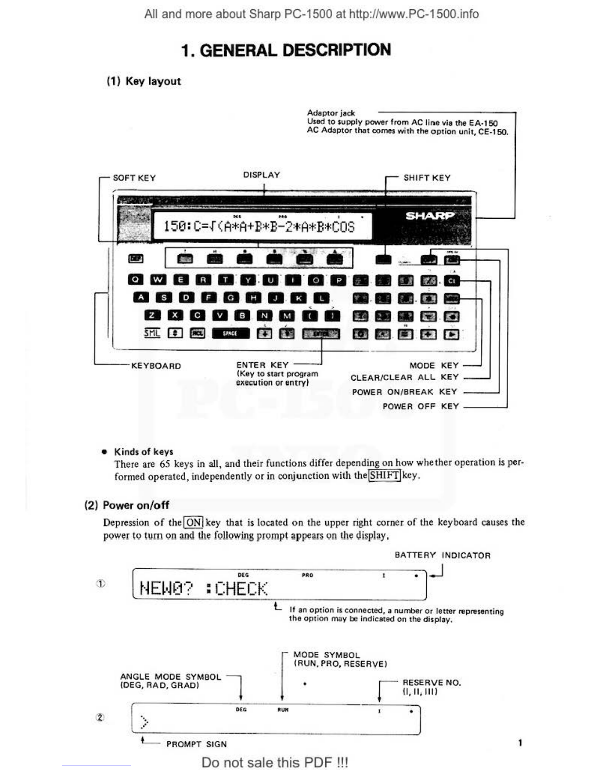
The
prompt shown
in
(
I)
appears afteran operation such
as
battery replacement.
The
pocket computer needs to
be
reset
in
the following manner, when the prompt shown in (E)
aippears
on
the display.
I
CL
I
NEW
O IENTERI "NEW
O"
is the command to reset
all
pock
et
computer conditions
to
their initi
al
states.
Upon
completi
on
of
above operation, the
pr
ompt
sign
shown
in
(2)
is brought on the display.
Abo,
depressing the lONI key after turning
off
the power with the
lO
FFI key brings the same
prompt on the display.
However, involvement
of
a failure in a peripheral
will
put a check
message
such as "CHECK
6-
"
on
the display,
if
any peripheral is connected
to
the pocket computer.
• Auto power off
With
this pocket computer the power is automatically shut
off
to
save
power, unless a key
entry is made within
seve
n minutes after the last key entry.
Depression
of
the
ION
I key after automatic turn-off
turns
the power on to the pocket
computer, then the machine and display conditionsretu
rn
to
what they were imediately before
the power was shut
ofC.
(3) Specifications
Capacity:
Operating sequence:
Programming language:
Central processing unit:
Memory configuraton:
Powerconsumption:
Physical dimensions:
Weight:
Accessories:
(4) Options
10digits (mantessa) +2 digits (exponent)
Direct formula entry (furnished with priority determining function)
BASIC
CMO
S 8-bit microprocessor
ROM:
16KB
RAM
: 3.5KB
System area:
Jnput buffer area:
Stack area:
0.13W
0.9KB
80
bytes
196 bytes
I95(W) x
86(0)
x 25
.5
(H)mm
375g, including batteries
Soft
case
, two templates, four batteries (type AA), instmction manual,
applica
ti
ons man
ual
and name label.
• CE-150 color graphic printer (built-in cassette interface)
The
CE-ISO
is the 4-color graphic printer that incorporates the cassette interface unit.
As
ball
point pen type
of
stylus
is
used for printing, four varieties
of
colored pens (black, blue, green,
red) can be installed and controlled
by
the proaram to draw either a straight
or
broken
li
ne
from
any
desired
locati
on
by
the
co
lor
designated.
Co
mbinat
i
ons
of
co
l
ors
a
nd
lines
will
ena
b
le
th
e formation
or
colorful graphics and any desired figure.
The
CE-150
can
al
so be used to print
program lists and data outputs.
Two tape recorders may
be
connected
at
the same time with the CE-I
SO
, one can
be
used
for
recording and the other for data transfer. For instance, today's data can
be
summarized and
recorded
in
one tape recorder, while transferring the data
file
of
yesterday from
th
e other tape
r
eco
r
der.
• CE-151 memory module
The CE-
ISi
is
the RAM chip of 4KB used to expand the program and
da
ta storage
of
the
PC
-1500.
o
When
th
e CE
-1
51
is
mounted
in
the
PC
-1500, the capacity
of
program and data storage is
expanded
to
5946 bytes.
• CE-152 cassette
tape
recorder
The CE
-1
52 is the ca'sette tape recorder exclusively designed
for
use
with the pocket compute:r.
Storing previous prog
ra
m and. data
on
tape
usiJ
1g the
CE-
15
2 as theexternal memory device
of
thePC-I
SOO
wi
ll
enable you
to
use the data again.
2 Note tltat
it
needs the CE-I
SO
color graphic printer to use the CE-I S2 cassette tape recor
der
.
Do
not
sale this PDF
!!!