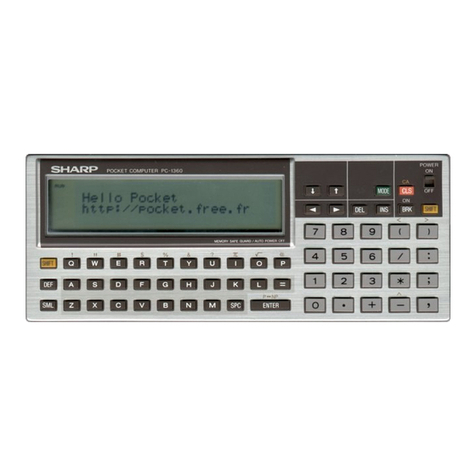
Sharp PC-1350 User manual

LCD display
(1) Text display
5 x 7
dot
matrix (24 x 4
lines)
(2) Graphic display
150 x 32 full
dot
display
Character size:
4.01 (H) x 2.85(W) mm
Character pitch:
3.48
(1
dot
space) mm
Dot size:
..ni '""
I
l1'i"3
'"4-LQ.05mm
r2?J
~=10.53mm
H~
0 0
~~~
•Display:
•Serial
i/
o
funct
i
on:
Communicat
i
on
method
:
Asynchronous (half-duplex
only
)
Baud rate:
300,600,
1200
Parity
bit
:
Even, odd, free
Word
length
:
7 or 8 bits
Stop bit:
1
or 2 bits
Connector:
15
-
pin, for
connec
-
tion with external
unit
Output
signal level:
CMOS level (4-6 volts)
Interfacing signals:
Input: RD, CS, CD
Output:
SD, RS, RR, ER
Others: SG, FG, VC
•Memory protection:
Program,
data,
reserve areas are
backed up by
battery
during power
off.
BASIC
CMOS 8-bit CPU
40 Kilobytes
System area: Approx. 1.6 kilobytes
Data area: 208 bytes
Program
/
data
area
:
3070
bytes
Rese
r
ve
area
:
144 bytes
Subroutine
:
1
0 stages
F
OR-NEXT: 5 stages
Funct
i
on
:
1
6stages
Data: 8 stages
Fundamental:
Four math rules
Functions
:
Trigonometric
,
reverse trigono-
metric,loga
r
ithm,
exponential,
angular
transformation,
power
rising, square
root,
integer, abso-
lute
value
,
signum
function,
circular
constant
Hor
i
zontal cursor
contro
l
(""
.
'4)
Insertion (INS)
Delet
i
on (DEL)
Line up and down
I
.l
,
t
)
SHARP CORPORATION
•
Editing
functions:
•
Basic calculator
functions
:
•
Stack
registers
:
•
Programming
language
:
•Microprocessor
:
•
System ROM:
•
Memory capacity:
•
Arithmetic
capac
i
ty
: 1
0
d
i
g
i
ts
(
man
tis
sa
)
+
2 digits
(
exponent
)
•Ar
i
thmet
i
c
method
:
In
o
r
der
o
f mathematical expres-
s
i
on
(
with
prior
i
ty
determination
f
unct
i
on)
P
C
-1
350
!
11
#
$
%
&
?
>r
I
@
8~~0~00~0~0
l
oErl
GJ
0 [£] [!] 0
GJ
GJ
[TI
CD
c:J
P
-
NP
@MW
0 0 ~ 0 ~ 0 ~ ~
I
ENTER
I
S
ML
~~
~~~~~~~~~~
~~~~~~~
l';HIIT
DEF
GRAPHIC 150
x
32
dot
OJ
[!]
TEXT
24
x
4 lines
POWER ON
Foo
E
I I
cc
L
~
I
[l
ON
O
FF
8J
[8
l
nEL
I
l
!Ns
l
IBRKI
~
< >
0~GCJ0
0G~DD
GJ000D
"
GDGDD
R
UN
PRO
CE-516L
CE-202M
CE-201M
PC-1350
MODEL
CODE:
OOZPC1350SM
/
E
•Mode
l
•
Keyboard
layout
1.
SPECIFICATIONS
SERVICE
MANUAL
SHARP -
PC-1350

S
I
O
15PI
N
P
E
R
I
F
E
RAL
llP
I
N
-2-
HM6116
2KB
X
2P
CS
RAM
R
OM
2
32
K
B
S
C
6
1
3256
FM
56
,......___~.._,,__
r.
L __
LLL
1
Vee
s
Di
Ai
:
Vee
Di Ai ~
g
b
1
Yz
I
1
l
I
I
I
OPTI
ON
RA
M
C
ARD
I
:
8
KB
/
16K
B
:
I
C
E
20
1M
/202
M
I
~
---
~L J
CR20
S
2
x
2
PCS
!B
i
KOi
Disp
l
ay
Dr
ive
!
Ai
s
soo
KE
Y
M
ATRI
X
LCD
H
1-8
l
50X32
D
O
T
H9
-
!6
LF-7II7E
3.
PC
-
1350 BLOCK
DIA
G
RA
M
*2: Memory
retent
i
on period of
the
CE-201
M
is
about
34
months
and
CE
-
202M
about
18
months
.
CE-126
P
24
-
digit
therm
a
l
printer
I
CE-124
cassette
.
:
tape
record~er
interface unit
I
I
a
L-----
-
-
- ~@]
CE-152
cas
se
tt
e
ta
p
e
re
c
or
d
e
r
--
~--
D
RAI
cm
B
D
Rll
CARI
16
EU
I
I
[9
PC
-
1350
-- portable computer
i
II
1
1::.::
~
>-
•••••
I
rr
-----------·····
1
••••••••••••••••
1
-
-
-
....
.
...........
I
-
.....
CE-202M
RAM
c
ard
*
2
CE
-2
0
1
M
RAM
ca
rd *2
0.03 watts
182(W) x
72(D)
x
16(H
)
mm
190
grams
,
including
batt
er
ie
s
Ha
rd
c
over, 2
templat
es, 2
l i
thium
b
att
er
i
es
co
nt
a
ine
d
i
n
t
h
e
uni
t,
i
ns
t
r
uct
i
on
manual
,
nam
e
l
ab
el
(
Exampl
e)
CE-124 Cassette Interface (CE-152)
CE
-
126P
P
ri
nt
e
r
/
Ca
s
sette
Interface
CE-201
M
8
KB
RAM card
CE
-
202M 16
KB
RAM card
2.
SYSTE
M
C
ON
FIGURATION
•
Opti
on
s
0
to
40
°
C
6VDC
(
CR20
3
2
li
th
i
um
battery
x
2
)
Abou
t
250
h
o
urs (when *5
*
dis-
played
co
n
t
in
u
ously
o
v
er
4
8
di
g
i
t
s
unde
r
20
°
C
.
B
ut,
i
t
may
v
a
ry
depending on
t
he
ki
nd
of
ba
ttery
used and
usage.
)
•
If
operat
e
d
on
e hour
p
e
r
da
y
,
it
will
l
ast
for
2
.
5
mont
h
s
,
pro
-
vided
that
10
m
i
nutes are used
for
ar
i
thmet
i
cal
operation
or
program
e
xecution
w
i
th 50
minutes of
d
is
play
i
ng
data.
•
Power
cons
u
mption
:
•Phy
s
ical
dim
e
nsion
s:
•W
ei
gh
t:
•
Ac
c
esso
ri
e
s
:
About
11
minutes
•
Batte
r
y
l i
fe
:
•
Auto
-
power-off:
•
Ope
r
at
in
g
temperature:
•
P
ower
s
up
p
ly
:
-
P
C
-1
3
50

Since
the
program
contained
in
the RAM card
is
retained
in
the
card after removal of
the
ca
r
d from
t
he
PC
-
1350
,
it enables
to
use the program again when
the
RAM card
i
s
mounted
i
n
the
PC-1350
afterward.
•
Becau
s
e
the
re
s
erve ar
e
a
is
i
n
th
e
PC-1350
,
it
is
no
t
poss
i
ble
t
o
r
es
e
rve
i
t
i
n
the RAM
ca
r
d.
....
s:
t
::T
Prog
r
am
(1) (1)
Jl
3
-0
a
)>
Q
cc
s:
-c
Cl
C')
:i
3
QI
a:
a.
--
---
-
--
-
-
-
-
-
-
-
-
--
-
-
- -
- -
-
-
-
~
....
s:
Array variables
a
nd
QI
::T
QI
(1) (1) simpl
e
variab
les
~
-0
3
QI
00
•
.!...<
w :i
U'l
F
i
x
e
d
var
i
abl
e a
r
ea
0
•
The PC-1350 wil
I
not operate
u
nless the RAM card
l
ock
s
witch
is
turned
t
o the
LO
C
K
s
ide.
•
When the data-free RAM card
is
i
nstalled
to
the
PC
-
1350
,
it makes the
PC
-
1350 memory
are
a linked
w
i
th
t
he RAM card memory area so
that the
program
/
data
area
is
united.
And, the program
is
w
r
itten from
the
RAM
card
,
and the array variables and simple variables
are secured by
the
PC
-
1350.
6. CAUTIONS
IN
USING
T
HE RAM
CAR
D
OPTION
FFFFH
7EOOH
8
000H
60
00H
6800H
7000H
7000
H
7!00
H
7200H
7300H
7
400H
7500H
7600H
7
700H
7
800H
7900H
79FFH
-
4000H
2000
H
8
K
B
i
nt
ernal
R
OM
I
8
K
B
RAM
16
K
B
card image
I
RAM
ca
rd
/
D
I
S
P
I
B
KB
D
I
SP
1
i
m
age
DI
SP
2
R
AM
c
ard
D
IS
P
2 image
R
AM
I
DISP
3
RAM
2
DI
SP
3 image
DI
SP
4
D
ISP
K
E
Y
p
o
rt
OIS
P
4
i
mage
D
I
SP
5
D
I
S
P
5
imag
e
No
t
u
s
ed
32
KB
K
E
Y
port
ROM
OOOOH
5.
RAM map
-
-
P
C
-1350
-
3
-
NOTE
:
To
replac
e the
battery
fo
r
th
e RAM card
If the RAM ca
r
d
i
s
replaced while it
i
s
installed
i
n
th
e
PC
-
1350
,
r
e
placem
e
nt
can be done w
i
thout
destruct
i
ng the
prog
r
am
da
t
a
.
ti
H
ow
t
o
j
udge the life
of
the
b
a
t
te
ry
PC
-1
350:
Need
s
r
eplac
e
m
e
nt
wh
e
n
the terminal voltage
d
rop
s
below
5
.
2
vo
lts
(
2
.
6
vo
lt
s
per
batt
e
ry
c
e
l
l).
CE
-
201
M
/
202M
:
N
ee
ds
replacem
e
nt
when the terminal
vol
ta
g
e drops
b
e
low 2.5 volts.
A
s
the
abov
e
v
al
ues
a
r
e
o
b
s
erved
un
der the
r
oom
t
em
-
per
a
t
u
re
o
f
20
°
C,
i
t
may vary
de
p
en
d
i
ng on
env
i
ron
-
ment
.
Power consumed
fo
r
the
PC-1350 20
µA
,
max.
under
powe
r
off
Power consumed for
the
PC
-
1350 500
µA
,
max
.
du
ri
ng
d
i
splay
i
ng
Powe
r
c
on
sumed
fo
r
the
PC-
1
350 5 mA,
max
.
during arithmetical
operat
i
on
P
o
wer consumed
fo
r
t
h
e
CE
-
202M
About
8
.4
µA
,
max.
ti
Powe
r
consumption
ti
Se
e
t
he
Inst
ru
ction
Ma
n
ua
l
fo
r
the
battery
l
i
f
e
.
Co
n
dition Date
retention
time
PC
-
1350
unde
r
powe
r
o
ff
About
7
months
PC
-
1350
+
CE202M
About
6 months
CE-201M
About
34
months
CE-202M
About
18
months
ti
Ba
tt
e
r
y
I
ife
PC
-
1350
Lithium
battery
,
Capacity
:
Terminal voltage:
power
supply
t
yp
e
CR
-
2032 x
2
pcs 200 mAH
Abou
t
6
.
0 V
CE
-
201M/ Lithium
battery
,
Capacity
:
Te
r
minal
voltage
:
202M
type
CR
-
2025 x
1
pc 120 mAH
About
3
.
0 V
4.
BATTERY LIFE AND
POWER CONSUMPTION

-4-
NOTE
:
The
contents of the
data
/
program
a
re
a
of
the
RAM
is
not
g
u
ara
n
teed
afte
r
the
e
xecution of
the test
prog
ram. It
needs
to
push
the
ALL RESET switch upon
the completion
of
the
t
e
st
.
Test ROM Key
op
e
rat
i
on
(
RUN mode) Successful
test
display
(
V.
1
)
CPU internal ROM (8 KB) CALL
&
8020
ENTER
31887
CPU
externa
l
ROM (32 KB) CALL
&
802A ENTER
2
1946
Tools required
_
....
_
..
8 KB
test
program RAM card (UKOGC1010CSZZ)
1
/
0 circuit test connector
cable
(
U
KOGG0089CSZZ)
•
PC-1350 implemented memory
test
program
I
n
the
PC
-
1350 ROM are
contained
t
he
check
su
m
test
programs
to test
the CPU
i
nternal ROM (8 KB)
a
nd
the
ext
e
rnal
ROM (32
KB)
.
~
(1)
3
~
!'
(1)
z
3
-c
0
(")
....
'
<~
Q)
w
....
(11
(1)
0
Q)
t
Program
-----
-
-
--
-
----
---
-
-
-
-----
Progr
a
m
A
rra
y
var
i
ab
le
s
and
sim~
e
var
ia
ble
s
F
i
xed
var
i
abl
e
a
re
a
o
Q)
a.
•
When program
is
executed
by
the
RUN
command,
it
makes array variables and simple variables
erased
.
To
make
the
RAM card
data
left on
the
card, define
the
program using
a
definable key,
then start the
program
with
that
definable key. Do
not
use
the
RUN
command.
•
If
a program
is
contained
in
the
PC
-
1350 upon mounting
of
the
RAM card, it makes the existing program ignored.
Therefore,
it becomes impossible
to execute the
program
contained
in
the
PC
-
1350.
Neither
,
it can be recalled. In
case a large sized program exceeding
the
RAM
ca
r
d
capacity
has been
contained
,
i
t
makes
the
program
i
n
th
e
PC-1350
destroyed.
Further
,
storing
o
f
a
r
ray variables
and simple
variab
l
es in
the
PC
-
1350 may also
mak
e
th
e
program
destroyed
,
depending on
the
case
.
(If
the
program has
not
been
destroyed,
it enables
yo
u
to execute the
program
after
remov
i
ng
the
RAM
card
.
)
This
prog
r
am
is
assumed
not
existing so
that
i
t
makes
the
program
started to
write, and,
when it
r
eaches
the
area
,
it
makes
the
program
destroyed.
Also
,
the
area where array
variables and simple variables
are stored
is
r
eached,
it
makes
the
program
destroyed.
As the
PC-1350
program/data
ar
e
a
i
s
not
used unless
the
M
EM
"C
"
command has been
executed
,
it
does
not destroy
t
he
program
.
7.
USE OF TEST PROGRAM
•
Setup by
the
MEM
"C" command
can
b
e
released by
the
execution
of
the
MEM
"B" command.
At this
point,
all
existing array variables and simple variables will be
e
r
ased.
•
When
the
RAM card
i
s
removed from
the
PC-1350
after
the
execut
i
on of
the
MEM
"C" command,
i
t
makes this
setup
invalid
to the
PC-1350
.
Howeve
r
,
mount
i
ng of
the
RAM card
to the
PC-1350 again will validate this setup.
3
:;
(1)
3
-c
0
Q
<~
Q)
(11
;;;
0
Q)
Array
var
i
ab
l
es
and
simple variables
•
~
(1)
Q)
Program
t
n
Q)
a.
•
How
to
hold
data
on
the
RAM card
Since variables such as array variables and simple vari-
ables are
transferred
from
the
PC-1350,
they
are erased
when
the
RAM card
is
removed from
the
PC
-
1350
.
However, it
is
possible
to
hold
the
variables on
the
RAM
card using
the command
(MEM
"C").
Execut
i
on
of the
MEM
"C"
command
makes variables held
on
the
RAM
card,
so
that they
remain on
the
RAM card even
after it
has been removed from
the
PC
-
1350
.
f
Th
i
s
a
r
ea
is
n
ot
us
e
d when
i"'"""'~u..u..""""'J..Lt..J.'-'-'-'-t.LLL..'-l.t.Li.
"<U.
J
'
MEM
"
C"
' is
execut
e
d
.
PC-1350 with CE-201M
PC
-
1350 with
CE
-
202M
CE-201M only CE-202M only
11262
8142
19454 16334
•
Capacity (bytes) of
the program/data
area
-
PC-1350

Returns
t
o
t
h
e
starting
point
.
-
5-
Table
-
1.
------~
D
i
spl
a
y
(
5
)
Ex:
"2
9
"
represents
the
[ID
key
.
[
ENT
E
R[
Keys
which
shou
l
d
ha
v
e
beenpressedare
displayed using
the
i
r
c
o
de
.
Make
r
eference
to
At
judge (5)
is
checked
i
f
I
E
NTER
I
key
ha
s
b
e
en
pressed.
keys are pressedin
the
g
i
ven
order
.
keys are pressed
i
n
the
given
order
.
A
t
judge (2)
is
check
e
d
i
f
OJ
ke
y
h
a
s
D
i
splay (4)
I
ENTER
I
been
pressed
.
R
U
N
PRO
1'
T
S
M
L
S
H
I
FT
DEF
Display (3)
.
...
.
.
.
.
.
(
S
ee
T
able-2)
.
. .
.....
.
~
.
~"
111•1111•
~~~~~~ ;
.~:J,~~;,:~:
[ill-
ffir
[IJ
-+
l
~
H
N
J-1
]
}.[j] At
judge (1)
is
checked
if
K
e
y
o
p
eration
Displa
y Remark
CALL
UOO
I
ENTER
I
~~"
111111111111111111•
1
::~::::~::~:~~~~
.
D
i
splay
C
f)
-
P
res
s
ke
y
•
Display and key input tests
Se
t
t
he
t
e
s
t
RAM card
(
UKOGC10
1
OCS
ZZ)
in
the
PC
-
1350.
Start
the
test
in
r
eference to the following
fl
o
w
c
hart.
-
-
PC-1350

-6-
With the above test program
ch
e
ck to
see
that the SIO
c
i
r
c
u
i
t
is
functioning properly with the
same
display appearingon
both
sides
.
90
:
CLOSE
:
GOTOl 0
100:END
90
:
CLOSE:GOT010
100
:
END
•
1/0 circuit tests
Make the 11-pin connector connected with the
CE
-
126P and
tl-
e
15
-
p
i
n
connector
of
the SIO
circuit
connected with
another
PC
-
1350 via the interfacing cable (UKOGG0089CCZZ). Perform communication with the other end to check
proper
function
i
ng
of
the
PC
-
1350.
(Programon the
te
st
ed
un
i
t) (Programon
th
e
testing unit)
10:
OPEN
10
:
OPEN
20
:
FOR 1=3T0255
20:
FOR 1=3T0255
30:
B$
=
CHR$
I
30:
A$=CHR$
I
40:
INPUT
#
1A$
40:
PRINT
#
1A$
50:
PRINT
#
1
B$
50:
INPUT
#
1
B$
60:
WAITO:PRINT A$;
60
:
WAITO:PRINT
8$
;
70:
NEXT
I
70
:
NEXT
I
V
80
:
C
LS
80
:
C
LS
(Table
-
2)
8-[J-0--
End
u
(Key entry sequence)
(Tab
l
e-1)
u
Display Corresponding Display Corresponding Display Corresponding Display Corresponding
code key code key code key code key
00
y
10
L 20
*
30 8
01
H
11
ENT
21
I
31
R
02
N
12
p
22
(
32
F
03 DEL
13 =
23
w
33 v
04 INS
14
24
s
34 0
05
15
SHIFT 25
x
35
1
06
u
16
DEF 26
+
36 4
07 J
17
SML 27 37
7
08
M
18
'
28
6
38 T
09 MODE
19
29
9
39
G
QA
lA
2A
E
3A
B
OB
I
lB
)
28
D
38
....
QC
K
lC Q
2C
c
3C
~
OD
SPC
1D
A 2D
•
3D
,),
OE
CLS
lE
z
2E
2
3E
t
OF
0 lF -
2F
5
3F BRK
(Key code chart)
-
PC-1350

-7
-
Pin No. Signal name
In
/
Out
Description
Standby=
power
off
1
A01 Out
(AO) Address bus line. High during standby.
2
R
/
W
Out
Write
clock
.
Normally
high.
3
cj>
AL Out Low
order
bit
address latch.
Normally
h
i
gh
.
Clock used
to
latch
the low
order 8
b
i
ts sent on the data
bus line which
is
usedin sending 16 bits addresssignal when using
a
large capacity ROM.
4 TES In Test pin
.
Normally
low.
5
¢
1
In
Osc
i
llator
input
.
6
¢
0 Out
Osc
i
llator output.
7
RES In Reset
input
.
Res
e
t
wh
en
high.
Normally
pulled down
to low
level.
8
X
i
n
In
CE
-
124 microcassette tape recorder
option
signal
i
nput
(MTin)
.
9 ON In ON
[BREAK]
key
i
nput
.
Normally
pulled down
to
l
ow
leve
l.
jBRKI
10
Xout Out
CE-124
m
i
crocas
s
ette tape recorder
option
and buzzer signal
output
(MTout1
)
.
11
Dis
Out
LCD
dr
i
ver
control
signal.
12
HA Out
LCD
d
r
iver
clock
.
Low
during standby
.
2 KHz pulse generated
during
d
i
sp
l
aying.
13 IAB
In
/
Out Key signal
i
np
u
t/
key
st
r
obe
output
signal.
Low
during
standby
.
Pu
l
se
generated when key
is
pressedin
the
low
level.
14
IA7 In/Out
Key signal
i
nput
/
key strobe
output
signal
.
Low
during
standby
.
Pulsegenerated when key
is
pressedin
the low level.
15
IA6
In
/
Out
Key signal
input
/
key strobe
output
signal.
Low
during standby
.
Pulsegenerated when key
is
pressedin
the
low
l
e
vel.
16
IA5
In
/
Out
Key signal
input
/
key strobe
output
signal.
Low
during standby. Pulsegenerated when key
is
pressedin
the
low
level.
17
IA4
In
/
Out
Key
s
i
gnal
input
/
key strobe
output
signa
l.
Low
during standby. Pulsegenerated when key
i
s
pressedin
the low
level
.
18
IA3
In
/
Out
Key signal
input
/
key strobe
output
signal.
Low
dur
i
ng standby. Pulsegenerated when key
is
pressedin
the
low
leve
l.
19
IA2
In
/
Out
Key signal
input
/
key strobe
output
signal. Low
dur
i
ng standby. Pulsegenerated when key
is
pressedin
the
low
level.
20 IA1
In
/
Out
Key signal
input
/
key
strob
e
output
s
i
gnal.
Low
dur
i
ng standby. Pulse
gene
r
ated when key
is
pressedin
the
l
ow
leve
l.
21
188 In
ACK
signal. Enable signal when
the
1/0 (PCU) readsdata
from
the
CPU
.
22 187 In Data In (Din)
s
igna
l.
Se
ri
al data
input
signal
from the
PCU
(bit term
ser
i
al handshaking).
23 186 In SIO
[CD]
.
D
e
t
ec
tion of
a
send request
from
the
other
end.
24 185 In SIO
[
CS]
.
Dete
c
tion of
send
enab
l
ed
from
the
other
end.
25 184 In SIO
[RD]
.
Re
c
eive
data
.
26 183
Out
SIO
[RR].
Sendi
ng
of
rec
eive enabled
from
this
end
.
Low during
standby (buffered by gate alley).
27 182
Out
SIO
[RS
].
Send
i
ng
of
s
en
d request
from this
end
.
Low during
standby (buffered
by
gate alley).
28
181
Out
SIO
[ER].
Goes high by the
e
x
ecut
i
on
of
OPEN command.
Low
dur
i
ng standby (buffered by gate
alley)
.
29
VM
In LCD power
supply
.
30
VA
In LCD power supply.
31
GND In Power supply
32
H1
Out
LCD
backp
l
at
e
signa
l. High
impedan
c
e
dur
i
ng standby
.
4
-
level pulse
dur
i
ng displaying.
33 H2
Out
LCD backplate signal. High impedance
during
standby. 4-level pulse during
displaying
.
34 H3
Out
LCD backplate signal. High
i
mp
e
dance
during
sta
n
dby
.
4
-
level pulse
dur
i
ng
d
i
splaying.
35 H4
Out
LCD backplate
s i
gnal.
H
i
gh
i
mpedance
dur
i
ng standby.
4
-
level
pu
l
se
during displaying.
36 H5 Out LCD backplate
s i
gnal.
H
i
gh
i
mpedance
during
standby. 4-level pulse
during
displaying
.
37 H6
Out
LCD
backpla
t
e
s
i
gnal. High impedance
during
standby
.
4
-
level pulse during
display
i
ng
.
38 H7
Out
LCD
b
a
ckplat
e
signa
l. High
imp
e
dance
during
standby. 4-level pulse
during
display
i
ng
.
39 HS
Out
LCD
backpla
te
signa
l. High impedance
during
standby
.
4-level pulse during
disp
l
ay
i
ng.
40 H9
Out
LCD
backp
l
a
t
e
signal. High impedance
during
standby
.
4
-
leve
l
pulse during
display
i
ng
.
41
H10 Out LCD backplate
s
i
gnal.
H
i
gh impedance
dur
i
ng standby.
4
-
level
pu
l
se
during
d
i
splay
i
ng
.
42 H11
Out
L
CD
backpla
te
signal
.
H
i
gh
i
mp
e
da
n
ce
during
standby
.
4
-
level
pu
l
s
e
during
displa
y
ing
.
43 H12
Out
LCD backplate
s
i
gnal. High impedance
d
u
ring
standby
.
4-level pulse during displaying.
44 H13 Out LCD backplate
s i
gnal
.
High
i
mp
edance
during
standby
.
4
-
leve
l
pulse during displaying.
45 H14
Out
LCD
backplat
e
sign
al. High
i
mp
e
dance during standby.
4-leve
l
pulse during
display
i
ng
.
46 H15
Out
LCD backplate
si
gnal. High impedance
during
standby
.
4
-
level pulse
du
r
ing
displaying
.
SC61860A 13 microprocessor signal
description
8.
LSI DESCRIPTIONS
-
PC-1350
-
8
-
P
in
N
o
.
S
ignal name
In
/
Out
D
es
cription
Standby
;
power
off
47 H16 Out LCD
backplat
e
s
i
gnal.
H
i
gh
i
mpedance
during
s
tandby
.
4
-
level pulse during
di
s
playing
.
48
V
s
In LCD power supply. High
during
standby
.
Clock stop
l
eve
l
in
Vs
state.
4
9
V
o
rs
In LCD power supply. High
during
standby. Clock stop
l
evel in
lo
w
state.
50
V
ee
In
L
C
D power
s
upply
.
Low at all
times
.
5
1
Vo
e
Out LCD power
s
upply
.
High
dur
i
ng standby. Clock stop
le
v
el in
low
state
.
52
V
GG
In Power
supply
.
Low
at all
times
.
5
3
08
I
n
/
O
ut
Data bus
line
.
Normally
hig
h
imp
e
dance.
54
07
In
/
Out
Data bus lin
e
.
No
r
mal
l
y
h
i
gh
imp
e
dan
c
e.
55
06
In
/
Out
D
a
ta bus
li
ne
.
Norma
ll
y
h
i
gh
imp
e
dance
.
56
05
In
/
Out
Data
bu
s
li
n
e
.
Normally
h
i
gh
imp
e
dance.
57
0
4
In
/
Out
Data bus
line
.
Normally
high
impe
d
ance.
5
8
0
3
In
/
Out Data bus
l
i
ne
.
Normally
high impedance.
59
02
In
/
Out
Data bus
line
.
No
r
mally
high impedance.
60 01
In
/
Out Data bus line.
Normally
high
imp
e
da
n
ce
.
6
1
F05 Out
32 K ROM
c
hi
p
enab
le
.
-
62
F
0
4 Out SIO
[
SD
]
.
Transm
i
t
data.
Low
during standby (buffered by gate
al
l
ey).
63
F
0
3 Out BUSY signal. Interface
output port.
64
F02
Out DOUT (Data
Out
)
.
Data
output
por
t to
peripheral
.
65
F
0
1
Out
Applica
t
ion ROM
c
hip enable
outpu
t
(provided on the RAM card
connector).
66
808
O
u
t
RAM,
DISP
-
LSI
enabl
e
signa
l.
67
80
7
Out (A14) addr
e
ss
bus lin
e.
High during
s
tandby
.
68
80
6
Out
(A13) addressbus
line
.
High during standby
.
69
805 Out
(
A
12)
add
res
s
bus
I
i
n
e
.
H
i
gh
du
ri
ng standby.
7
0
804
Out (A11) addressbus
li
ne
.
H
i
gh during
s
tandby
.
71
80
3 Out (A10)
addr
e
ss
bus
l
i
ne
.
High
du
r
ing standby.
72
80
2 Out (A9) addr
e
ss
bus
l
ine. High during standby
.
7
3
8
0
1
Out
(AS) address
b
u
s
line
.
H
i
gh during
s
tandby
.
74
A08 Out
(A7) addressbus
l
i
ne
.
High
dur
i
n
g
st
andby
.
75
A07 Out
(A6)
addr
ess
bus
line
.
High
duri
ng
s
tan
dby
.
7
6
A
06
Out (AS)
add
r
ess
bus line.
H
i
gh
du
r
ing
st
andby
.
77
A
05
Out (A4) addressbus
line
.
H
i
gh
dur
i
ng
s
tandby
.
78
A
0
4
Out
(A3) addressbus
line
.
H
i
gh during
s
tandby
.
7
9
A
0
3 Out (A2)
addre
ss
bus
l
ine
.
High
dur
i
ng
s
tandby
.
80
A
0
2
O
u
t
(A
1)
addressbus
li
ne. High during
standb
y.
-
P
C-
1350

-9-
-
-7
.
0V
NOTE
:
Voltage whenVD
IS
=
7.0 volts
-+-
-
5.
6
V
-
-4
.2
V
-
-2
.
8
V
-
-1
.4V
-
ov
S
tate of retention
during power off
Power
of
f
(
CP
U
standby)
-
PC
-1
350
L(
RE
S
E
T
O
N
~
~
·
-
V
A
,__
V
M
-
V
B
-
G
ND
·V
A
H-
t
VMH-
I
*
VB
H
__..:I
D
1
s
VD
ir
s
/5
VAL
-
t
V
D5I
S
%
V
D
IS
V
ML- f
l
VD1s
V
D
!
S
-
5
-
·VBL-
.J.
h5
1._1
-----'
(
S
H26:TR5
)
ES
R.H
:
TR22
Display on
T
h
e
LCD
oper
at
es
un
d
er
1
/
1
6
duty
.
8
0
-pin
"
·
-
-
..
-
- -
-
...
..
-
..
- -
....
-
- - -
......
-
-
..
-
-
..
-
....
-
-
-
- - - -
-
- -
..
..
-
-
·
C
E
Ofj}-
R/W
~
(
S
63
)
S63
0
1
-s
~
~-~
Q
Ss1
Q
S
s2
'
'
'
(
S6
2
)
S62
64
by
te
(
80-B
F
)
M M
co
6 4
b
y
te
(
4
0-
?
F
)
R
e
ad
/
Write
ho
;
h
, ;
h,
;
h,
;
h
,;
h,
I
I I
I I
Vors
VA
V
s
S1
S
2
¢AL
DI
S
Displ
a
y
out
•
Ti!llin
g
(
(Latch clock)
Descript
i
on
of
the SC43537 Display
LS
I

-
10
-
h5
=
1
h5
=
0
All
d
i
git
s
off
(DIS
=
L)
V
A
L
V
s
H
O
n
V
s
L
V
AH
O
ut
V
A
L
VsH
ON ON ON
ONOFFOFFOFIFdFFOFFOFFON
ON ON ON ON ON ON ON
OFF
A
ll
d
igits off
VD! S=VBL .._
S
egme
n
t w
avefo
r
m
VML
-.
VBH
--
--
----~
B
ack
pl
ate
(H
1
)
wavefo
rm
VMH
--
---
····-····-··
-
-----
- -
-·
VAL
--
----
---i
G
ND=V
A
H
--
S
egme
n
t
out
p
ut waveform
H1 H2 H3 H4 H5 H6 H7 H8 H9 HlO
Hll
H12 H13
H1
4
H1
H
2
H3 H4 H5
- -
--
--
·
- -
--·-
-
··-
-
---
-
-
--
--------
-------------
--.
-
·····-·········-
··
-
····-
-
--------
----.
··
·-- ---
-
---
-
· ·
·----
----
-
-------,
hl
(
TRl
)
h2
(
TR2
)
h3
(
TR?
)
h4
(
TR4)
h5
(
TR5
)
DIS
RES
HA
•
Counter and segment waveforms
-
PC
-
1350

Vee
Inpu
t
b
u
ffer
-
11
-
.,_
R....:O....:M
~
N
ot
use
d
(F05
i
nv
e
rt
ed
o
ut
put
)
To
the
S
I
O
connector
Key strobe
(P-typeopen
dra
in
o
u
tp
u
t)
RAM
Card
CE
R
A
M
1
CE
RAM2 CE
DI SP
1
CE
D
I
SP
2
CE
DI SP
3
CE
DI SP
4
CE
DISP
5
CE
OUT4
IJJ
RR
OUTl
IJJ
SD
OUT2
1JJ
ER
OUT3
IJJ
R
S
Un
i
t
c
el
l
...
....
•.'\
...
A1
4
~ OPCE
...
..
.....
..
...
A1
3
,_
R
A
M
l
_
...
A12
....
R
A
M2
:
...
,_
:
A
ll
-
..
Ad
d
r
ess
de
c
ode
r~
DE
1
...
~ AlO
,,
-
D
E
2
...
:- A9
"'
DE
3
...
-
...
....
,....
...
-
DE
4
...
-
....
-
DE
5
-
...
...
...
R
/
W
I
,,
A
...
D6
K07
...
....
D5
...
...
K0
6
-
,,
....
....
D
4
KO 5
...
,,
·
~
-
D
3
K04
....
....
D
2
D
ata
l
atc
h
....
...
K03
...
....
Dl
...
...
K02
...
....
DO
....
...
KO
1
...
....
....
C
P
U
Fr
o
m
signals.
SC60220 Gate
Alley
This LSI chip
is
used
to
decode various LSI (RAM, DISP) chip
s
e
lect signals,
to
generate key
strob
e, and
to
b
u
ffer SIO
output
BOS
-
PC-13
5
0
•

-
1
2
-
F
lat
p
a
c
kage
LS
I,
CE
-
201
M
a
nd
CE
-
202M
PCOS
ty
pe CE-202M
With the PCOS
type
CE-202M it should be stable below
7
.
0µA.
W
i
th the
flat
package
LSI
CE
-
202M it should be stable
below 8.4
µA
.
Although several ten microamperes may flow
immedi
-
ately after power
on,
i
t
can be disregarded.
DC
suppl
y
(
3
V
)
W
i
p
e
cl
ean
th
e
b
o
ard
a
nd
t
h
e
c
a
bin
et
ta
pe bonding
port
io
n u
si
n
g
a
l
c
o
ho
l.
Aft
e
r
bo
nding
,
w
i
p
e
t
e
rm
i
nal
s
using alcohol.
o
Wh
en
re
moved in
t
h
e
dir
e
ct
i
on
C
<B
e
Ba
t
t
e
ry pad
DC supply
(
3V)
CE
-
201
M
/
202M power
consumption test
1)
Connect the ammeter between both ends of
battery
pad
(see figure below).
2)
Turn on the +3V DC supply and measure the
amperag
e
after
three
seconds later.
3) With the CE-201
M
the amperage should be stable below
4.0µA.
Bonding the curled terminals on the
cabinet
may result in
terminal
contact
failure. Make the deformed board
unit
corrected so
that
a slight degree of curl should appear in the
opposite
direction,
and use the fresh tape
to
bonding the
board on
the
cabine
t.
(How to remove the board)
Pay
attention to
the
following
when removing the board
unit from
the cabinet
for troubleshooting.
*
PCOS
board
:
The board on which an
LSI
ch
i
p
is
directly bonded.
Model name Type Parts code RAM
LSI
CE
-
201M Flat package LSI
DUNTK8066CCZZ
2KBRAM x 4 PCS
CE-202M Flat package LSI
DUNTK8200CCZZ
2KBRAM x 4
PCS+
8KBRAM x
1
PC
PCOS
board" DUNTK8045CCZZ --
•
There are
two
kinds of RAM card options available with one CR2025 lithium
battery;
the one
is
the
CE
-
201
M
which has 8
KB capacity and
the other
is
the
CE
-
202M which has 16
KB
capacity
.
•
As the lithium
battery
is
contained
in
the
package
,
it must be
fitted
using the special
battery
removing tool
that
comes
with
the
RAM card.
•
There are following kinds of board units.
o When removed in the dire
c
tion
B
•
9. RAM CARD
-
PC-1350

-
1
3
-
N
(T)
~
-
-
-INm·~
...:)
< (D Q '
11.J 11.J 11.J 11.J
u.J
>>>
>
<r
O
QQOO
0
w
LL
l}
}}}}])}))J~)))
~
~
.
~
i
1
~1~1~1~1
~
1
~
1
~
1~1~1~1~1
~
1
~
1
~
1~
1u
0 3:
...:i
-
-
-
- - - -
-
- - -
- --
-
- - -
-
-
<<<<
<<
<<<<<<
<<
<<<
<
<<
i.n
"4"
"'
"4"
'4' '4' "'
"4"
"'
"4" "4"
"' '4' (l'l (l'l (l'l - - - -
I
I I
'
t
•
I I
I
•
I I
I I
I I
1 1 I I
!::::!::::~~
~~
!::::!::::~!::::~!::::!::::
~
!::::!::::~~~~
~
·
~
e-
<Xl
u ~ u
~
rl
>----<
>--
-
-~
t--
-----
~
J
J
~
tttl
~l
:;l
--
-----
-
<«<
<<<<<
roi
,...,
roi (l'l N N N N
'
t I I I
I
I I
N
N
NN
NN
NN
-
--
---
-
-
r- "'
Lil
....
m N -
CD
r- "'
Lil
....
1Tl
N -
CD
Lil ....
- N m -
....
Lil "' z
CD
r- "' Lil
....
1Tl
N - m N
z
I-
CD
r-
o o o o o o o o o o o o o o o o o ow
CD CD
O
CD
ID
CD
O <
<
-e
< < < < < o o - =i
a::i a::i
!DCDCDCD.:OCD
!D«
«<<<<<
<
r:ou...u...--
-
u...--
-
~--
--
--
-
-u_
u_xo-
-
u
:r:
-
-
-----
<
...
<
...
< <
..:
--
NNNNN
'
I
<
I
I I
<
N
NNNNNN
-
---
-
--
T
;!
c;
"'
~
¢c~
L-+
~~
-1
f-
-+-
-
-~~
:
!
-
j
.--
~-"'
'Vv-
-~
mN
~
><
r--OOO'lo-
N
ll'l-:-111\Cl
r-
CDC"l
o
1,[]
-
N
OO
r--'°LllLll
.,,.m
"''""
Lll
\O
r-
OOC"le>m._,. o-N
'°\O\O
r-
r-r-r-r-r-
r-r-r-r-
co
-
\O"''ON
NN
\O
NN
NC"l-
------N
\O\OCIO
-NN
/
...-
"1 N - o
--
--
-
O'I
CO
r-\O
lfl
-..P">
N
-o
<<<c<<
<
<<<<<<<<
~
'--
-----------~
+--4-+-+-+-~-+-
~~~-
_.
~--
~-+-
~
+-+
-
-+--+--
-.-
~
l
;:
LI
...-
..-iN-o ID
CD
Lll-N"1...-
Ll-Nm'4'Vl\,(;r-
--
-
--C"l;l::
~
OZZZZ
Z
> 0 0 0 0 0 0 0 < < <
... ... ...
-
a:
co
- - - - -
Ll
-
NWLll ...
1TlN
-
r-\OLll
....
fT1N-
Lil
_,.
1'1N-O
u
z::
l:::u1-1-
1-1-1-o
oooooou.;ww
w
w
z
> < < ~ =i =i ~ ~ =i
r
r r r r r ro o o o o ~
a:
a:ooo
oo
o
r-N
-
Plt"-1'1
-4"
Lll'V-C>C"ICI0\0Lll
....
N"1
....
Lll\OOO
- -
--
N
trlP">mmNN-
-
- --NNNNNP'>
kl kl kl kl kl kl kl
I
~
1
m m
""
m
z z z z
c
z
-
....
0
1Tl
-'""-
N
1TlL/l
CD
--
r--
!
I I
I t
I I I I I I
NNNNNNNNNNN
z z z
z
z z
z z
z z z
LlLI
LI
U
UUUULI
LI
U
~
r
~
·
~
~
cc~c
,;
u
~~
L
z
0:
0:::
W Vl (r LI U LI :> Vl IL 0
~
:;
r- ~
ru
,
'
"'
a:J
.~
:I
u
..
'ij
::)
e,
o
c
Lt)
M
<>::
....
u
e,
...:
u
0
w
LL
l'.l
:r:
PC-1350
10. CIRCUIT DIAGRAM (1)

<(
u
0
L'.J
(\J
~
0 0 0 0 0
~
u 0
~
;
e
~
>
~
< < < <
~
~ ~
~ ~
<
~
:; :; :; :; :; :; :; :;
~
~
~
~
~
~
~
~
~
~
-
1
4
-
lf)
=
=
=
= =
=
=
= =
=
= =
::
=
~ ~
~
~ ~
~
~
c :;
;o
~
';'
~
':'
~
~
':'
';'
~ ~ ~ ~ ~ ~ ~ ~ ~
f
~ ~ ~
~
- N m ~ m ~ ~
oo
~ o - N m ~ m ~ ~
oo
~ o - N m ~ m ~ ~
oo
m m m m m m m m m
~
~
~
~
~ ~ ~
~
~ ~
m m m m m m m m m
m m m m m m m m m m m m m m m m m m m m m m m m m m m m m m
lJ.J
~
w
~
~
~
(\J
u
0
:c
lf)
CIRCUIT DEAGRAM (2)
-
PC-1350

CD
~
...
·:;
u
...
·c:;
>
ca
Q.
"'
:c
0
in
M
...
<(
c.)
D..
N
ID

<(
u
w
I
N
(Y)
-1
5
-
l[)
..
z z
LI LI LI LJ LI
~~~~~
~
- -
-
- -
z
u
~
))))))))
I
-c
°'
=
0..
i:
~
~
'.J
~
~
I
I~
I
~
'4'
P">
N - Q
O'>
en
r- 'O
U1 _,.
"1
NNNN
--
--
-
--
-
PC-1350

~1:;;
~;;;
~
~
z;
:;;l;;t;{~
1
~1~1~1~1'.;1~
l
~1~1'.;
1
~
~
~
~:;::;::
Z
N Z Z Z Z Z Z Z ZZ z Z Z Z ~
:;
':;
~ ~ ~
::;!
~
:; ~ ;;
0
~
>
c_ __
--+--
~
u
uuuuuuuuuuuu
zz
zzzzz
zz
zzzz >
l[) (Y) N
u u
~
'
~
>
:?:
0
a:
co
u
w
LL
CIRCUIT DIAGRAM (3)
.~
e
·u
>
...
0
E
Cl)
E
0
in
~ <(
u
Q.
M
\
\

-16 -
N
...
-c
y y y y y
-
-
-
- -
- - -
y
~
>
~
~
~ ~
~
~
~ ~
~
~ ~ ~ ~ ~ ~ ~
-
-
en
"'
.~
::I
e
...
'(j
><
·
;:
'Iii
E
c
(.)
..J
.._
>
Q)
~
0
Ll)
M
...
u
0..
.,j
~
x
Cl'.'.
f--
"
...
:i::::
~
~
co
)---
~
co
w
~
~
~
~
z
~
~
l'.J
91HX
- - - - - - -- -- -
--
--
- - - - - - - - -
-
---
---
-
---
--7(
9
1
H
l'.J
SlH*
-
- -- - --
-
-----
-
--
------,
1'lH)(
- -- -
--
-
-
-
---
----
- --- ---,
I
--
7<
>IH
I
E
l
HX- ---- --
-
- ----
-
-
----- -
I
I
1
-
----
---
--7(
EI
H
I I
I
Z
l
H)E-
-
---
-
-
-
- - - - - -
-
-
-
----,
I
I
I I
,-
------
-7(
Z
l
H
I
I
I
I
I
I
ll
H
l l
H)(
- - -----
----
------!
I I
I
I
I
I
r--
---
-x
O!HX
-
- - - - --
-
------
-
--
1
I
I
I
I
I
I
I
I
1
--
-
-
7<
OI
H
I
I
I
I
I
I
I
I
6H*
--------------,
I I
I I I
I
I
I I
I
,----
-7(
6H
Cl'.'.
I I
I
I
I
I I
I
I I
I
I
0
I I
I
I I
I
I I
I I
I
I
f--
I
I
I
I I
I
I I
I
I I
I
LJ
I
I
I I I
I
I
I I
I I I
u, w
OS
l
S
OOES
u,
z
6!7
l
S
662S
z
Bl>
l
S
B62S _'}
0
D
l
S
L62S
LJ 971S 9625
C>
S\P
IS
5625
u
H
I
S
7625
__J
~
LS
LS
I
S
9S
9S
I
S
SS
S
SIS
'5
\'S
I
S
ES
ESIS w
ZS
2S
lS
IS
I
Sl
S
OS
,
-
~
I I
I
I I
I
I
I
I I I
I
I
I
I
I I
I I
I
I
I
I
I I
I
I I
I
I
L
___ ,
I
,-
-~
I
I
I I
I
I
I
]
__
_
I
-
-
~
I I I
I
I
L
_
_,
I
I I
I
I
,
-
~
I
I
I
I
l
_
_ ,
I I
I
I
I
,
-
~
I
I I
I
_
__
I
I I
I I I
I
f--
I
I
I
I
I
I
I
I
I
I
u,
L
_
_
I
I
I
I
I
I
I
I
z 0
__J
u,
I
I
I
I
I
I
I
C>
I I I
I
IH)(
-
_J
I
(/)
I
I
]
______
___
--?<
B
H
I
I
I I
I
I
I I
C>
2H* __
_J
I
I
I
I
I
I
L
--
---
-
-
-
--
7<
LH
C>
I
I I
I
EHX----
_J
I
I
L
_
---
-
-
- ----
-
--x
9H
I
I
I
I
?H)(
-
--
--_J
I
I
I
I
__
_
___
__
__
__ -
-
-7<
s
11
I
I
I
SH)(
- - -- -- _
_J
I
I
I
-
-
-
---
-
-------7<
>
H
I I
91-l)f-
---
------
-_J
I
I
I
i
'
.
==
=
=
===
=
==== ~===
:
::
L
HX-
-
---
-
--
-- -
-
--
_J
I I
I
I
BH)(
-----------
-
-
----
_J
L-----
-
-
-
-
-
-----
-
------
7<
IH
v
LJ LJ
CIRCUIT DIAGRAM (4)
-
PC-1350

T._
K
ON
V
GG
-17 -
IA
7
}
oFF
key
-----I
A
8
It
is
the
circuit
to prevent change in the RAM card contents
which may occur when the RAM card
is
replaced in the
following condition:
(1) during
auto
-
power-off,
or
,
(2)
with
the PC-1350
i
n
power on
cond
i
tion
to
replace the RAM card.
f
S
W2
L
oc
k
S
W
Jumper
and
subsidiary
board
circuitdescription
1
1.
PARTS AND SIGNAL LAYOUT CHART (MAIN PWB)

-18 -
-KoN
-IA7
}
OFF
k
ey
-IA8
(
1)
During
auto-power
-
off
A pulse
is
sent
through
KON
to actuatethe
PC-1350
when
the
card cover lock switch
is
manipulated,
and,
at
the
same
time,
the OFF key
is
activated
to turn
power
off.
(2) During displaying
or
run
A pulse
to the
BRK key line (to KON) by
the
lock
switch
to
release
the
PC
-
1350 from running
state
(BREAK
action),and,
at
the
same
time,the
OFF
k
ey
is
activated
to turn
power off.
ion
iption
I
AM card
contents
is
replaced in
the
-IA8
·-:
·
x,:&i
,
.
Kon
-
PC-1350
*
1
:
M5
-
M7
us
i
s
activated
to turn
power
o
f
f.
T._
K
ON
VGG
(1) Dur
i
ng
auto
-
powe
r
-off
A
pulse
i
s s
e
nt
t
hrough KON
to
actuat
e
th
e
I
when the card cover lock switch
is
manipulated
t
he
sam
e
ti
me
,
t
he
OF
F
k
ey
i
s
ac
ti
vated
to
t
u
r
o
ff.
(
2
)
Du
r
i
n
g
display
i
ng or
r
un
A
pu
l
se
to the BAK
key
li
ne (to KON) by
1
s
witch
to
releas
e
the
PC
-
1350
fr
om
r
unn
u
(BREAK
action), and, at
the same
time, the
C
IA
7
}
oFF
ke
y
----
IA
8
following
condition
:
(
1
)
during
auto
-
power-off,
or
,
(
2) with
the
PC-1350 in
power
o
n
condition
t
o replace
the
RAM
card.
f
S
W2
Loc
k
S
W
I
t
i
s
the
circu
i
t to prevent
change
i
n
t
he RAM
ca
r
d
'
wh
i
ch may occur when
t
h
e RAM card
i
s
r
eplace
'
J
umper
and
subsidiary
board
cir
c
uit description
-19 -
f
Parts and signal
layout chart (memory
PWB)
-
PC-1350

-20-
*
1 :
M5
-
M7
us
e
d
for
the 2SA
1179
.
::?
::?
0
a:
LL
ne (to KON) by
the
lock
1350 from
r
unning state
e same
time
,
the OFF key
f.
>N
to
actuat
e the
PC
-
1350
i
tch
is
manipulated, and,
at
1
i
s
act
i
vated to
turn
power
(O
N
A7}
OFF
key
A8
in condition
!
in the RAM card
contents
,
M
card
i
s
replaced
in
the
uit description
Table of contents
Other Sharp PDA manuals

Sharp
Sharp PC-1500 Product manual

Sharp
Sharp TM-20 Quick start guide

Sharp
Sharp Zaurus SL-5500 Manual

Sharp
Sharp YO-P20H User manual

Sharp
Sharp Zaurus SL-5500 Quick start guide

Sharp
Sharp Zaurus SL-5500 User manual

Sharp
Sharp PC-E500 User manual

Sharp
Sharp PC-1360 User manual

Sharp
Sharp PC-1246 User manual

Sharp
Sharp Zaurus SL-5500 Quick start guide

Sharp
Sharp Zaurus SL-C3000 User manual

Sharp
Sharp PC-1500 User manual

Sharp
Sharp PC-1500 Product manual

Sharp
Sharp PC-1600 User manual

Sharp
Sharp PC-1403 User manual

Sharp
Sharp Zaurus SL-5500 User manual

Sharp
Sharp PC-1403 User manual

Sharp
Sharp PC-G850VS User manual

Sharp
Sharp EL-6890 User manual

Sharp
Sharp PC-1285 Assembly instructions