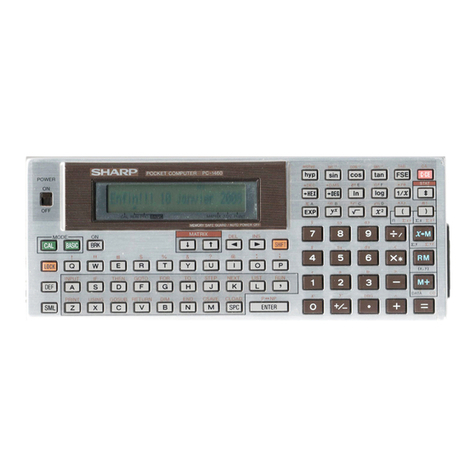
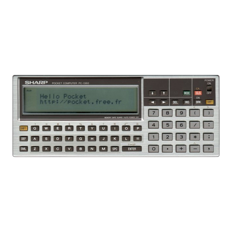
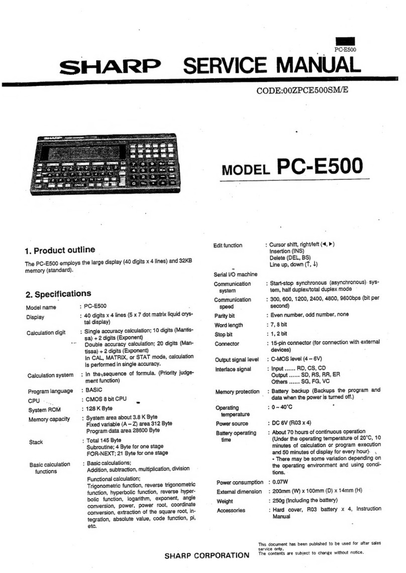
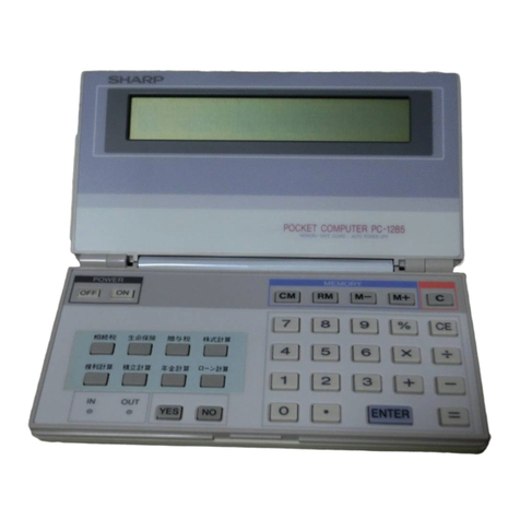
Sharp PC-1246 User manual

•
Ba
s i
c
2
KB RAM
S
y
st
e
m
a
rea
:
0800H
-
OAFFH
U
ser
a
r
ea
:
OBOOH
-
OFFFH
•E
x
pan
sio
n
2KB RAM
(PC
-
1
2
4
7
on
l
y
)
Al
I
o
pen
for
u
se
r
ar
e
a
2000H
r------,
: :
2K
B
,
exp
a
n
sio
n
2
7FFHL----
-
'
(PC
-
1
2
47
o
n
l
y
)
~8
b
it-'1
o
_
sooHI
_
I
2
K
B
,
basic
1
0 FF
F
H
'---------'-
SHARP
CORPOR
A
TION
3
7FFH
I
J
r-10
bi
t
---i
MAIN
ROM
14K
s
tep
x 10
bi
t
(
17Kb
yte
s
)
[
CPU
interna
l
ROM
] [
E
x
t
e
rnal
RAM
]
OOOOH
....--
-
--~
3
.
MEMORY
MA
P
Auto
power
o
ff time
:
Approx
.
11
minutes
Options:
CE-124
,
C
E-125,
~E-126P
,
CE
-
152
16-characte
r
l
i
qu
i
d
c
ry
s
tal
dis
-
play
with
5
x
7
do
t
cha
r
act
e
rs
(LF7133E)
Character
dimension
s
:
4
.
5(H) x
2
.
7(W
)
mm
Character
pitch
:
3.45 mm
0
°
C
~
40
°
C
(32°
F
~
104
°
F)
6V DC
Lithium
c
ells
Type
:
CR-2032
App
rox
.
1000
h
o
u
r
s
(D
i
sp
l
ay: 55555555,
amb
ie
nt
tempe
r
ature
:
20
°
C
(
68
°
F
).
The
operating time
s
l
igh
t
ly
var
ie
s
depending upon the
use
of
battery.)
Battery
will
last
fo
r
a
pe
r
iod
of
2.4
m
o
nth
s
,
assuming
t
he
us
e
of
on
e
hour
a
day
w
h
i
c
h
consi
sts
of
10
m
i
nute
s
of
op
er
at
i
on or pro-
gram
e
x
ecution and 50
m
i
nut
e
s
of
d
i
splaying.
0.07
w
135(W) x 70(D) x 9.5(H )mm
5
-
5
/
16"(W) x
2
-
3
/
4"(D)
x3
/
8"(H)
95g
(with
cells)
Weight
:
Power
Consumption
:
Dimensions:
Operating Time:
Display:
~"'"'
0.01~~
o.~~~
w~
.
0
5
0.5
Operat
i
ng
Temperature
:
Powe
r
Supply:
PC-
1246
PC
-1
2
47
OOZPC12
4
7
SM
/
E
MODEL
CODE
Memory
P
r
otection
:
E
d
i
t
i
ng
F
e
atu
r
es
:
Basic
calculations
:
Add
i
t
i
on
,
s
ubst
r
act
i
on
multi
-
pl
i
cation, division
Funct
i
on calculations:
Trigonometric
and inverse
trigonometric
functions, loga-
t
i
thmic
and exponential func-
tions, angle
conversion
,
square
root, interger,
absolute
,
sign
operators
,
tt
.
Cursor
left
and right
(
>
,
<
)
r
character
inse
r
t
(INS)
,
character
delete
(DEL),
line up and
d
o
wn
(
i
.
t
)
Battery backup (the contents of
programme and its data
are
retained at
power
-
off.)
Operators:
10 stacks
5
stacks
16 stacks
8 stacks
Sub
-
rou
ti
ne:
For
-
NEXT
:
Funct
i
o
n
:
Data
:
Stack
:
Programming Language:
CPU:
System ROM:
Memory
Capacity
:
Calculating System:
10 digits (mantissa)
+
2 digits
(exponent)
Algebric system
(with priority
judgement
function)
BASIC
4
bit
CMOS
17.4K bytes
System Area
About
0.5K bytes
Area dedicated
to
data
208 bytes
Program
/
data
area
1278 bytes (PC-1246),
3326 bytes (PC-1247)
Calculating Capacity:
2. SPECIFICATIONS
PR
I
NfUSJM;GOSUBRETIJRN
D
I
M
E
ND
CSAVE
C
LOAD P...+NP
0 0 ~ 0 ~ ~ ~
D
l
rnTER
I
S
P
C
INPUT
!
f
1HEN G01D FOR TO
STE
P
J\'EXT
L
I
ST
RUN
0
~
@.l0@JGJ
[TIIBJ(g~
!
!I #
$ ~
&
?
:
'
:
@J0000~
@l
[i]@J
0
D
E
G
RAD
G
RAD
RU
N
P
RO
S
HI
FT
E
I
I
B
US
Y
p DEF
P
O
WER
OF
F
C=:]
ON
ON
~ [I] [I] ~
DE
L
I
NS
~ [3J [TI ~
POCKET
CO
MPUTER
SHARP
1. KEY LAYOUT
SHARP -
P
C
-1
246
SERVICE
MANLiAl

-2-
Pin Signal
In
/
Out Function
standby=
power
off
No. name
1
V1 In LCD
driv
i
ng power
2
V2 In LCD driving power
3 V3 In LCD driving Power
4 V4 In LCD
d
r
iving Power
5
V5 Out
E
x
pansion RAM chip
enable
,
normally high, (Not used
w
i
th the PC-1246.)
6 VDD Out LCD drive power, high during standby.
7
GND
In
Power supply
8
VGG
In
Power supply, normally low
9 X1 Out System clock oscillation
output
10 X2 In System clock oscillation
input
11
X3 Out
D
i
splay clock oscillation
output
12 X4
In
Display clock oscillation
input
13
K1
In
Key
input,
normally low
14 K2 In Key
input
,
normally low
15 K3 In Key
input
,
normally low
16 K4 In Key
input,
normally low
17
K5 Out (SEL2) Select signal
output
18 K6 Out (SEL
1)
Select signal
output
19 K7 In ACK
s
i
gnal. Enables the
1
/
0
(PCU)
to
read data
from
the
CPU
.
20 KB In Data
in
.
Serial data input
from
the PCU
(bit
-
to-bit
serial handshake)
21
RESET
I
n
Reset
input,
normally pulled down to low level. Reset when high.
22 Cl
In
Option cassette tape recorder interface
input
23
co
Out Option cassette tape recorder interface
signal
/
buzzer signal
output
24
R
/
W Out Write clock, normally high
25
DI01
In
/
Out Data bus, normally low
I I
2
2
32 DIOB
In
/
Out Data bus,
normally
low
33
B1
Out Address
bus
,
low during
standby
.
Also
,
used
for
periphe
r
al
data
output port
(Dout).
2 2
2 2
43 B11 Out Address
bus
,
low during
standby
.
Also, used
for
peripheral data
output port
(Dout)
.
44 B12 Out Basic RAM chip enable
45 B13 Out Busy interface
output port
46 S40 Out LCD segment
signal
/
key
strobe
,
low or high during standby and 4-level pulse during
d
i
splay.
2
'
2
I
2
85
S1
Out LCD segment
signal
/
key
strobe
,
low or high during stnadby and 4-level pulse during
display
.
86 H16 Out LCD backplate
s
i
gnal
,
low or high during standby and 4-level pulse during display.
2 2 2 2
100
H1
Out LCD backplate
signal
,
low or high during standby and 4-level pulse during display.
•
CPU signal
descr
i
ption
A
100
-
pin
,
4-bit, microprocessor
used
in this model
has
a
17KB ROM and display chip
within
the
chip
.
What
it
differs
from
the
conventional microprocessor
is
that
i
t
has
no iternal RAM but
uses
an external RAM
for
execut
i
on.
4.CPU(SC61720D03)
-
PC-1246
PC-1247
-3-
I
!P
I
N
C
ON
NE
CT
OR
r=
L
C
D
LF7133E
!
i~i
H
,
I
H
I
H
I
H
I
H
I
H
I
H H
s s s s s s s
I
s
I
s s
s
1
1
s
:
l
s s
s
l
s
J
s
s
J
s s s s s s s s s s s s
s
1
1
s
s
1
1
s s s s
s
1 1
s s
I
s
1
6
I
2
3
4
5
6
7
I
2 3 4 5 6 7 8
9
10
11
1
2 13
14
1
5
1
6
17
18
1
9
20 40
39 3 8 3
7
36
35 34 3 3 32 3
1
30
2l
28
21
26 25
24
23 22
2
1
l
e
~iiii'
,f;'
,,..
J\1"
&&
tf.:
1%"&
d·
wlr
.JJlk
1
'ilil
,.,,
1
"1
l
it
@)
*'·•
'".dlk
i!iii
~ii.
:0
..
"''
'""··
.
j!;
""'""
'01\i
""''
,,;(t:lil
'"'·:ii!
!ll
.
1
0::;
b
il
ee
l
;
cc cc
:
I
U?
<D
~
~ ~
:
I
-
"'
~
1
"
~
l
<D
~
1
eo
gi
~
1
~
1
l"'
~
IJ
J~
ccr ccr
c-i
cc
r
cc cc cc
"'
"'
"'"'
cc cc
k
Cf'J
If) (f) (f) (/) in (/)
a:
(/) (fJ (fJ (fJ (fJ (fJ (fJ (/)
sn
in
(/)
(fJ
o:
(fJ
sn
(/) in (/)
(/)
sn
"---..§_§_
80
75 70 65
60
55
:~
~
00
~
1
·~1
"'
~
'-
~
:2
Ii~
H
!
6
Hl
5
:I H
!4
LS
I
1
e
H!3
i
wi
Hl
2
~
H
11
C
P
U
(
ESR
-
J)
!~
H
10
H9
H7
S
C6
17
20
D0
3
.
I
H6
"'
U?
H
5
~
<~
H4
H3
H2
UI
H
l
0
0
l
5
10
15
20
25
>
I
~
1
:;:
I
> u:
1
"'
~
8
;<
"'
1J
~
"'
co
"
"'
lTIJ
r
0
~
l
~
>
§'
c
>< ><
x
"'
"'
"' "'
~
~
:::c
~
~ u u
2 2 22
>
"'
R
9
1
80Kn
"'
"'"'"'"'
"'
I
U.C
'
?
Olp~
~
H
~
R
7
l.
3
M
!l
'---
R
3
>
R5
R
6
R
4
VR R9
X
I 10
24
KHz
47Kn
L6
l
.
8
}
\.<l
~
~Kn
~
~Kn
20
Kn
HOf--
r
l
r
•
2S
A
ll
79
C
9
1 1
O
.
l
u
F
C!O
I I
O.
l
p
F
-'-
rcloPF C2
,_
!
OOPF
C!l 11
0.
lp
F
c;
L1
o
0
.03
.....
~
E
R2
4
.7K!
l
µ
F
~~
.ro
m
'
~
GND
C
3
,_
V
G
G
DI
o.
1
p F
T
B
US
Y BIS
g
2
_
R
I
?2ll
DAN2Q2
::
~ ~
~
:
~
3
t
G
~
N
2
0
2
X2
xo
u
c
o
,
c,
C4
-
C
R20
32
K8
...:::._
(
3
VX
2
=
6V
)
--
22
p
F
/
DI
N
j'.
+
6
.
3V
ACK
K7
SE
L2
2
K5
Ri
l
O
RI!
S
E
L
1
K
6
,
;..
GN
D
Y 3
.
3
M
n
x
2
....,
-
PC-1246
PC-1247
5
.
PC-1246 CIRCUIT
DIAGRAM

-
4
-
D4
AB
B
9
A9
B
lO
R
/W
OE
AlO
B
il
CE Bl
D
S
B
S
A7
_
C2
_
!OO
P
F
B
7
A
6
B
6
A5
B
5
A
4
!
C
l
B
4
A
3
B3
2
KB
A
2
RAM
B
2
Al
B
l
AO
HM
6
116
D
l
D
2
D3
VGG
"'
;:;
"'
§5
gi
;i;
cc
cc
Ul Ul Ul Ul Ul
ifJ
65
60
55
51
s
36
0
"'
s
37
S40
B
l
3
~
B1
2
L
S
I
sn
B
10
B
9
CP
U
(
E
S
R-
J
)
0
8
8
-r
B7
B
6
8
5
"'
SC
61720D
03
B4
B3
"'
ON
cc
O
FF
R8
B2
!M
n
P
O
W
ER S
li
de
SW
B
l
D
l
O
S
1
5 20
25
cc
"'..,.
-
0
~
0
8
~ ~ ~ ~
u u
"'
0 0
M
l
SSS SSS SSS SSS
S
SS
S
SSS SSS SS SH HH HH
HH
H
30
29
28
27 26
25
2
4 2
3
22
2
1
15
1
4
13
1
2
11
1
0 9
8 7 6 5
4 3
2
l
16
1
5
14
13
12
11
10 9
s
s
35 34

r
z
0
-
1-
-
(/)
0
a.
(/)
...J
'
<t
z
e
-
(/)
~
(/)
l-
a:
~


-7-
3.3
M
n
x2
11
P
IN
C
ON
N
E
C
TOR
..i..
GN
D
R
ll
,i.,
C
4
--
22pF
/
+
6
.
3V
-
CR2
032
-=..
(
3VX2
=
6V
)
C3
..._
DJ
O
.
l
p
F
T
DAN202
I
RI
22n
~
MTO
U
T2
<;>----+---1--~
GN
D
)
V
GG
! >-----11----~
B
U
5Y
\--
DOUT
c)>-----
N
~
20
:
2
1--+-+-+-'
XI
N
c)>------~
·
03
_+--'
XO
U
T
)>-------+---'
D
I
N
X>----
-
-~
1
ACK
rX>-------'1
SE
L2
§r
,_
-'1
SE
Li I
R
,
2
,
.
4.
71\!l
D2
N202
'J
Tr2
R1
4
2SC28
12
4.
7K!l
'-
~~
2
R12 R9
1
8
01\!l
¥1
lO
O
K!l
I
'
.
I
UH~
Buz
ze
r
o
. 1
p~i:
H ~
li
R
5
R6
R4
~
1 1
,
8
.I
<fl
W
<n
~
6
.
Kn
R3
25A
l1
79
C9
I I
0
.
1'F
R
13
47Kn
l
O O
K!l
C
lO
I I
O
.
lpF
c
n
1 1
O.
lpF
2
5
0
0
-
1
5
10
1
5 20
-
""
~
r
io 0 ~
,.
;< ""
~
~-
""=
~
l
ffi
~
>
>
> > >
~
c:
~
x x x "'
"' "'
"'"'"'"'"'
C)
ifi
"'
°'
'-''>....
R
7
l.3M!l
'-----
YR! Xl
10
24
2
0K!_l
KH
z
Hrn-
-'-
?do
PF
C2
lOOP
F
c
;
Lt
0.03
µF
~
E
Hl
H2
H
6"'
H5
"'
H4
SC6
1
72
0D03
H7
H9
H
10
Hll
C
P
U
(
ES
R
- J)
H
l
2
0
"'
H
1
3
LS
I
1
H14
H
l
5
60
65
7
0
5
1
::?.;
~
5:
r-
~
5
:
r-
5
,
r-
B
~
-
~
~
B
f-
il
l
r-
0
B
:
~
-
B
'
>----
~
B
l
r-
B
·
>----
~
~
..§.:
B
E.
_D
a
o
co
~
55
l
~
_s
o
75
'
54 00
r
,111
~
.{
~
'- "----2.!_~
H
l
6
s
s
i
s s s
s
i
s s s s s s
s
i
s s 5
s
s s s
s
s 5 s s s 5 5
s
s
l
s
l
s
l
s
l
s s
11
1
21
1
3
14
1
5
16
11
1
1
8
1
9
20
40
39
38137
36 3 5 34
sa
3
2 3
1
so
3J
28 21
26
25
24
23
22
21
1
15
1
14
1
1
3
1
1
2
1
LF7
1
33
E
L
C
D
-
PC-1246
PC-1247
7.
PC-1247 CIRCUIT
DIAGRAM

8.
-
8
-
B
B
A7
GND
B7
AG
AB
B9
BG
A
9
BIO
A5
B
5 A4
IC!
R
/W
I
C2
B
4
A3 2KB 2KB
B3
A
2
RAM
RAM
B
A
l
B
H
M
G!IG
HMG
!
l6
AO
AO
DI D7
Dl
D7
D2
D6 D2
DG
D3 D5 D3 D5
vcc
D4
Vc;c;
D4
Bi
l
BIO
B
9
~
B
8
B7
B
G
B5
iii
B4
B
3
"'
ec
O
FF
R
8
B2 lM!l
PO
W
ER
S
l
ide
S
W
B
l
D
l0
8
SSSSSSSSSS
SSS
SSSSS
HHHHHHHH
2
3 2 2 2
1
15
1
4
1
3
1
2
ll
10
9 8
7
G
5
4 3 2
l
is
1
5
14
13
1
2
II
IO
9

z
0
-
t-
-
CJ)
0
Q.
CJ)
..J
<(
z
e
-
CJ)
~
CJ)
t-
a:

0
-
>-
~o
1-z
.... (!)
<(
a:i

-
11
-
I
I
II
I
I
I
I
Hl0
------
-
-------------1
I
H
9
--------------------
_J
Hl6
_]
I
I
:
H15·
-------
-
----_J
I I
H14
---------------1
I
H
l3
---------------_J
I
Hl
2
----------------_]
I
Hll
·
---------
-
-------_J
59
58
57
56
55
54
53
52
-~-
51
---
517
518
519
520
540
539
538
537
536
535
534
533
532
531
500
529
528
527
526
525
524
523
5:<2
HW--
------
-
-
---
-
-
------
--
-
-,
H
l
----
-
-----
--
-
--
--
---,
I
H2
--
-
----
-
-
----
---
-
--,
I
I
H3
·---
-
---
------
--
-.,..
,
I I
:
H4
------
-
---
-
----
-
,
I I I I
H5
--
-
-------
-
----,
I
I : :
I
H6
---
--
---------
1
I I I I
I
I
H7
·
--
----------,
I I : : I I
i
51
~
52
I
53
I
54
I
55
56
57
58
59
510
5
ll
512
513
514
1
0. LCD(LF7133E)
9-6.
Auto-power-off
check
Display must not
go
out
within
8 minutes but should go
out within
14 minutes.
9-4.
At
a
time
of
battery replacement
After
replacement of the
b
a
ttery, turn
pow
er on
a
n
d
push
the RESET
switch
.
9
-
3. RAM capacity check
Turn the slide switch
ON
,
pus
h
the
I
MODE
I
switc
h
to
go
into
the PRO mode. Enter
[NJ
[EJ
[WJ
[QJ
I
ENTER
I
and
[MJ
~
[ENTER]
to
have the
following
fig
ure on
the displav.
PC-1246
: 1
278
PC-1247
:
3326
+
Short
or
op
e
n
ON
with
GND
'\__J
O
N
G
N
D
At
the
t
i
me
of
on
w
i
th the
sl
i
de switch
a
t"
ON position
115µA at
V
G G
=
-0.6V,
m
axim
u
m
9-2. On current check
DC
r
egul
a
tor
circui
t
+
Shortthe OFF Pad
with
B11pad
GND
\___J
OF
F
Bll
A
t
the
t
i
me
of off
w
i
th
t
he
sl
i
de
s
w
i
tch at
OF
F
po
s
i
t
ion
7µA at
VGG
=
-
6
.
0V
,
maximum
9-1
.
Off
current check
-
PC-1246
PC-1247
9. CHECKITEMSANDCAUTIONS

-
12
-
NO.
PARTS CODE
PR
ICE
N
EW
P
AR
T
DESCRIPT
I
ON
PC
1246
P
C1247
RA
N
K
M
A
R
K
RANK
1
LPL
T
P
1
1
1
2
C
C
ZZ
AA
D
Ten
p
late
0 0
TiNS
J4
326CCZZ AT
N D
I
ns
t
r
u
c
t
ion book
(
J
a
p
an
)
0
2
T
iNSG4
330
CC
ZZ
A
K
N
D
In
s
t
r
uction book (G)
(
G
e
rm
a
ny
)
0 0
Ti
NSE
4328
C
CZ
Z
AR
N
D
In
s
truc
t
i
on book
(
E
l
(
O
the
r
countr
i
e
s)
0 0
3
TL
S
T
S
1
0
0 6
CC
Z
Z
AA
D
S
ervice list (Jaoan
t
voe onlv)
0
4
SPAKA
8990
CCZZ
A
E
N D
P
ackin
g
c
u
shio
n
for
se
t
0 0
SPAKC
899
1CCZ
Z
AD
N D
P
acking case
(
J
apan)
0
5
SPAKC
8993C
C
ZZ
AD
N D
P
ackin
g
c
a
se
(
O
t
h
er
co
unt
ries)
0
S
PAK
C
0
82
ACCZZ AD
N
D
P
ackin
z
c
a
se
0
~
Accessory
NO
.
PART
S
COD
E
PRICE NEW PART
DESCRIPTION
P
C12
46
PC1
24
7
RANK
M
A
RK
RANK
1
PZETL1313CCZZ AA
c
Sp
ac
er
(
Rou
nd)
0 0
2
PZ
ETL1
3
53CCZZ AA
c
S
pa
cer
(Squ
are)
0
3
QCNCW1306CC
1
B
AK
c
Con
n
ec
to
r
Cl
Z
o
in)
0 0
4
QCNTMl
0 5
l
CCZZ
A
B
c
R
e
s
et
t
e
rmin
a
l
0 0
5
QTANZ
1
2
8
9CCZZ AB
c
B
a
t
tery
t
e
r
m
i
na
l
0 0
6
RC-CZ1021CCZZ AB
c
C
a
p
acitor
(
0
.
1
u
F
)
[
C
3
,
5
,
6
,
9
,
l
0
,
1 1
]
0 0
7
RC-CZ10
3
5CCZZ AC
c
C
a
pa
ci
t
o
r
(1
OOpF
)
[
Cl
,
2
]
0 0
8
RC
-
CZ10
37
C
CZZ AB
c
C
a
p
aci
t
o
r
(
O
.
Olu
F
)
[C8
]
0 0
9
RC-CZ1
0
47
CCZZ AB
c
Ca
pacitor
(
0
.
033u
F)
[
C7]
0 0
1
0
R
C-
EZ
22
6BCC
O
J
AD
c
Ca
p
aci
t
o
r
(6
.
3WV
22u
F
l
[
C4
]
0 0
11
RC
RM
-
1
0 0
1
CC
Z
Z
AF
N
B
C
rv
s
t
a
l
(10
2
4KH
zl
[
X
l
]
0 0
1
2
RH
-
DZ
1
00
8
CCZZ AC
B
Diod
e
(DAN
20
2)
[
Dl
,2
3] 0 0
13
RH-TX1017CCN1 AB
B
Tran
s
i
s
tor
(
2SA1179
)
[
TRl
]
0 0
14
RVR-Z
2
400QCZZ
A
F
B
V
ar
i
a
ble
re
sis
t
o
r
(2
0K
O)
[
VR]
0 0
15
VHiHM
6
116
//-
C
AZ
B
IC
(
HM6116
)
[
ICl
2
]
0 0
16
VHiSC6
1
720
D0
3
BE
N
B
IC
(
SC61
720
D0
3
l
[
LSll
]
0 0
17
VRS
-
TP
2
BD105J AA
c
R
es
i
sto
r
(1
/
8W
I.
OM
O
±5%)
[
R8
]
0 0
1
8
VRS-TP
2
BD
1
3
5J AA
c
R
es
i
s
t
o
r
(1
/
8
W
l.
3M
O
±5
%
)
[
R
7] 0 0
1
9
VRS
-
TP
2
BD1
83
J
AA
c
R
es
i
sto
r
(1
/
8W
1
8K
O
±
5
%)
[
R5
,
6] 0 0
2 0
VRS-TP
2
BD1
8
4J AA
c
R
e
s
i
s
t
o
r
Cl
/
8W 18
0K
O
±
5%)
[
R9]
0 0
2
1
VRS
-
TP2
B
D
22
0J AA
c
R
esi
s
to
r
(
1
/
8
W
2
2
0
±
5
%)
[
R
l] 0 0
22
VRS
-
TP
2
BD335J AA
c
R
es
i
sto
r
(l
/
8
W
3
.
3M
O
±5%)
[
Rl0
,
11
]
0 0
23
VRS-TP2BD47
2
J
AA
c
R
esisto
r
(1
/
8W
4
.
7
K
O
±
5
%)
[
R2
14]
0 0
2
4
V
R
S-T
P
2
BD4
73
J
AA
c
R
es
istor
(l
/
8W
4
7K
O
±5%
)
[
R
3] 0 0
2 5
VR
S
-
TP
2
B
D
56
3
J
AA
c
R
esi
s
tor
(l
/
8W 56KO
±
5
%)
[R4] 0 0
2
6
RH-T
X
1012
CCZZ AC
B
Tr
a
nsi
s
tor
(
2SC
2
81
2)
[
TR
2
]
0
2
7
VRS
-
T
P
2
B
D104J AA
c
R
esis
t
o
r
(l
/
8W
lOOK
O
±
5
%
)
[
R
1213] 0
(Unit)
901
D
U N
T
K
8
2
1
7 C
C
Z Z
BP
N
g
M
a
i
n
P
W
B
uni
t
0
D
UNTK83
1
3CCZZ BS
N
E
M
a
i
n
PW
B
u
nit
0
[I]
E
l
ectronic parts
NO
.
PAR
T
S
CODE
PR
I
C
E
NEW PART
DESCRIPTION
PC
12 4
6
PC
1
2
47
RANK MARK RANK
1
X
BSS
C2
0P
0800
0
AA
c
S
crew
(2
X
8)
0 0
2
HD
E
C
A
2 0
8
2
CC
2
1
A
F
N D
B
o
tt
o
m
p
ane
l
0
HDE
C
A
2 0
82CC22 AF
N
D
B
o
tt
o
m
p
anel
0
3
P
ZETL15
5
6CCZ
Z
AA
N
c
B
o
tt
o
m
pane
l
shee
t
0 0
4
QT ANZ 14
0
6CCZZ AB
c
B
a
tt
erv
termi
nal
(
EB8
)
0 0
5
X
USSD
2
0P0
80
00 AA
c
S
c
r
e
w
(
2
X
8
)
0 0
6
LCHSS1
1
6
8
CCZZ AE
N
c
Cha
ssis
(J
a
pan
)
0
LCHSS1168CC
0
1
AE
N
c
Chas
sis
(
Other
co
untrie
s)
0 0
7
DU
N
TK
82
17CCZZ BP
N
E
M
a
in
PW
B
un
i
t
0
D
UNT
K
83
13CCZZ BS
N
E
Main PWB unit
0
8
PGUMS1564CCZZ AB
N
c Rubber
co
nn
ec
to
r
0 0
9
PSPA
P
1271CCZZ AA
N
c LCD
s
p
ac
e
r
0 0
10
VV
LL
F
7133E
/
-l AR
N
B
LCD
0 0
11
RA
LM
B1030CCZZ AD
B
Buzzer
0
1
2
PSLDP1486CCZZ AB
N
D
D
is
p
l
a
y
fil
t
e
r
0 0
13
PF
i
L
V15
2
6CCZZ AC
N
c
Po
l
ar
i
zed
filte
r
0 0
1
4
PGUMM1559CCZZ AL
N
B
Ke
v
r
u
bbe
r
0 0
1
5
QCNTM1042CCZZ AA
c Slide
s
w
i
t
c
h
termina
l
0 0
16
MSLi
P
1033CCZ
Z
AB
N
c
Sl
i
d
e
switch slider
(
J
apan)
0
M
S
Li
P
103
3
CC01 AB
N
c
S
li
d
e
s
w
i
tch
s
l
i
der (Other
countri
es)
0 0
DUNTG
8
215CCZZ
AM
N D
Top
c
abinet
(Ja
p
an)
0
1
7
DUNTG
8
21
6CCZZ
AM
N D
Top
ca
binet
(O
t
her countries)
0
DUNTG
8
3
1
2CCZZ
AM
N
D
Top
c
abin
e
t
0
1
8
GCASP
1
099CC
ZZ
AE
D
Ha
r
d
c
a
s
e
7
0ther
co
u
ntries)
0 0
GCASP1099CC0
2
AH
D
Ha
r
d
ca
se
(Jaoa
n
)
0
1
9
TLABH
2
095CCZZ AC
N
c
Op
e
r
a
t
ion
lab
e
l
(Japan
)
0
TLABH2096CCZZ AC
N
c Operation
l
a
bel
(Other
countrie
s)
0 0
2 0
PTPEH121
3
CCZZ AB
c
Ta
Pe
0
11.
PARTS
LIST
&
GUIDE
[I] Exteriors

1
8
14
-
13
-
19 17
-
PC-1246
PC-1247
I
ERRO
R GUI
DE
I
1
I I
i
I I
\
'
,
\
\
18
8~~
~
9
10
9
7
2

SHARP CORPORATION
Industrial Instruments Group
Quality
&
Reliability
Control Center
Yamatokoriyama
,
Nara
639
-
11
,
Japan
1
9
84
D
ecembe
r
P
r
i
nt
ed
i
n
Japa
n
®
SHARP
-
PC
-
1246
PC
-
1
24
7
This manual suits for next models
1
Table of contents
Other Sharp PDA manuals

Sharp
Sharp PC-1500 User manual

Sharp
Sharp Zaurus SL-5500 User guide

Sharp
Sharp SL-C1000 User manual

Sharp
Sharp PC-1600 User manual

Sharp
Sharp Zaurus SL-5500 Quick start guide

Sharp
Sharp PC-1500 User manual

Sharp
Sharp Zaurus SL-5500 User manual

Sharp
Sharp PC-1500A User manual

Sharp
Sharp PC-1500 Product manual

Sharp
Sharp EL-6890 User manual

Sharp
Sharp PC-E500 User manual

Sharp
Sharp PC-1460 User manual

Sharp
Sharp PC-1350 User manual

Sharp
Sharp SL-6000L User manual

Sharp
Sharp PC-1500 Instructions for use

Sharp
Sharp PC-1403 User manual

Sharp
Sharp Zaurus SL-C3000 User manual

Sharp
Sharp EL-6053 User manual

Sharp
Sharp ZAURUS ZR-5000 User manual

Sharp
Sharp Zaurus SL-5500 Quick start guide