Sharp XL-MP8H User manual

SERVICE MANUAL
XL-MP8H
No. XXXXXXXXXXXXX
MICRO COMPONENT SYSTEM
XL-MP8H
MODEL
SHARP CORPORATION
CONTENTS
This document has been published to be used
for after sales service only.
The contents are subject to change without notice.
CHAPTER 1. GENERAL DESCRIPTION
[1] PRECAUTION FOR USING LEAD-FREE
SOLDER ........................................................ 1-1
[2] SAFETY PRECAUTION FOR SERVICE
MANUAL ........................................................ 1-2
[3] SPECIFICATIONS ......................................... 1-3
[4] NAMES OF PARTS........................................ 1-4
CHAPTER 2. ADJUSTMENTS
[1] ADJUSTMENT ............................................... 2-1
[2] TEST MODE .................................................. 2-2
CHAPTER 3. MECHANICAL DESCRIPTION
[1] REMOVING AND REINSTALLING THE
MAIN PARTS ................................................. 3-1
[2] DISASSEMBLY .............................................. 3-2
CHAPTER 4. DIAGRAMS
[1] BLOCK DIAGRAM MAIN ............................... 4-1
[2] BLOCK DIAGRAM DISPLAY ......................... 4-3
CHAPTER 5. CIRCUIT DESCRIPTION
[1] WAVEFORMS OF CD CIRCUIT .................... 5-1
[2] VOLTAGE....................................................... 5-2
CHAPTER 6. CIRCUIT SCHEMATICS AND PARTS
LAYOUT
[1] NOTES ON SCHEMATIC DIAGRAM ............6-1
[2] TYPES OF TRANSISTOR AND LED ............6-1
[3] SCHEMATIC DIAGRAM MAIN(1/3) ..............6-2
[4] SCHEMATIC DIAGRAM MAIN(2/3) ..............6-4
[5] SCHEMATIC DIAGRAM MAIN(3/3) ..............6-6
[6] SCHEMATIC DIAGRAM DISPLAY ................6-8
[7] WIRING SIDE OF PWB ..............................6-10
[8] WIRING SIDE OF PWB MAIN TOP ............6-12
[9] WIRING SIDE OF PWB MAIN BOTTOM......6-14
[10] WIRING SIDE OF PWB POWER/JACK......6-16
[11] WIRING SIDE OF PWB DISPLAY/
SWITCH ......................................................6-18
CHAPTER 7. FLOWCHART
[1] TROUBLESHOOTING ..................................7-1
CHAPTER 8. OTHERS
[1] FUNCTION TABLE OF IC .............................8-1
[2] FL DISPLAY ..................................................8-7
Parts Guide
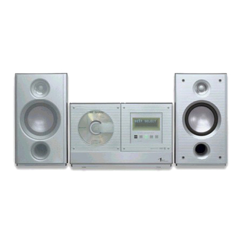
XL-MP8H Micro Component System consisting of XL-MP8H
(main unit) and CP-MP8H (speaker system).
•
In the interests of user-safety the set should be restored to its origi-
nal condition and only parts identical to those specified be used.
XL-MP8H
1 – 1
Home StereoXL-MP8HService ManualXLMP8H S/MMarketE
CHAPTER 1. GENERAL DESCRIPTION
[1] PRECAUTION FOR USING LEAD-FREE SOLDER
1. Employing lead-free solder
Example:
Indicates lead-free solder of tin, silver and copper.
2. Using lead-free wire solder
When fixing the PWB soldered with the lead-free solder, apply lead-free wire solder. Repairing with conventional lead wire solder
may cause damage or accident due to cracks.
As the melting point of lead-free solder (Sn-Ag-Cu) is higher than the lead wire solder by 40 C, we recommend you to use a
dedicated soldering bit, if you are not familiar with how to obtain lead-free wire solder or soldering bit, contact our service station
or service branch in your area.
3. Soldering
As the melting point of lead-free solder (Sn-Ag-Cu) is about 220 C which is higher than the conventional lead solder by 40 C,
and as it has poor solder wettability, you may be apt to keep the soldering bit in contact with the PWB for extended period of
time. However, Since the land may be peeled off or the maximum heat-resistance temperature of parts may be exceeded,
remove the bit from the PWB as soon as you confirm the steady soldering condition.
Lead-free solder contains more tin, and the end of the soldering bit may be easily corrected. Make sure to turn on and off the
power of the bit as required.
If a different type of solder stays on the tip of the soldering bit, it is alloyed with lead-free solder. Clean the bit after every use
of it.
When the tip of the soldering bit is blackened during use, file it with steel wool or fine sandpaper.
Be careful when replacing parts with polarity indication on the PWB silk.
Lead-free wire solder for servicing
Ref No. Description
Parts No.
PWB-A DCEKKV558SJ03
"
MAIN,JACK,SENSOR,SWITCH,DISPLAY,POWER
PWB" of this model employs lead-free solder.
The LF symbol indicates lead-free solder, and is attached on the PWB and service manuals. The alphabetical character
following LF shows the type of lead-free solder.
MAIN(A1)/JACK(A2)/Sensor(A3)/SWITCH(A4)/DISPLAY(A5)/POWER(A6)

XL-MP8H
1 – 2
[2] SAFETY PRECAUTION FOR SERVICE MANUAL
Precaution to be taken when replacing and servicing the Laser Pickup.
The AEL (Accessible Emission Level) of Laser Power Output for this model is specified to be lower than Class 1 Requirements. However, the follow-
ing precautions must be observed during servicing to protect your eyes against exposure to the Laser beam.
1) When the cabinet has been removed, the power is turned on without a compact disc, and the Pickup is on a position outer than the lead-in posi-
tion, the Laser will light for several seconds to detect a disc. Do not look into the Pickup Lens.
2) The Laser Power Output of the Pickup inside the unit and replacement service parts have already been adjusted prior to shipping.
3) No adjustment to the Laser Power should be attempted when replacing or servicing the Pickup.
4) Under no circumstances look directly into the Pickup Lens at any time.
5) CAUTION - Use of controls or adjustments, or performance of procedures other than those specified herein may result in hazardous radiation
exposure.
FOR A COMPLETE DESCRIPTION OF THE OPERATION OF THIS UNIT, PLEASE REFER TO THE OPERATION MANUAL.
VAROITUS! LAITTEEN KÄYTTÄMINEN MUULLA KUIN TÄSSÄ
KÄYTTÖOHJEESSA MAINITULLA TAVALLA SAATTAA
ALTISTAA KÄYTTÄJÄN TURVALLISUUSLUOKAN 1
YLITTÄVÄLLE NÄKYMÄTTÖMÄLLE LASERSÄTEILYLLE.
VARNING - OM APPARATEN ANVÄNDS PÅ ANNAT SÄTT ÄN
I DENNA BRUKSANVISNING SPECIFICERAS. KAN
ANVÄNDAREN UTSÄTTAS FÖR OSYNLIG LASER-
STRÅLNING, SOM ÖVERSKRIDER GRÄNSEN FÖR
LASERKLASS 1.
ADVARSEL-USYNLIG LASERSTRÅLING VED ÅBNING. SE IKKE IND I
STRÅLEN-HELLER IKKE MED OPTISKE INSTRUMENTER.
VARO! AVATTAESSA OLET ALTTIINA NÄKYMÄTÖN LASERSÄTEILYLLE.
ÄLÄ TUIJOTA SÄTEESEEN ÄLÄKÄ KATSO SITÄ OPTISEN LAITTEEN
LÄPI.
VARNING-OSYNLIG LASERSTRÅLNING NÄR DENNA DEL ÄR ÖPPNAD.
STIRRA EJ IN I STRÅLEN OCH BETRAKTA EJ STRÅLEN GENOM
OPTISKT INSTRUMENT.
Laser Diode Properties
Material: GaAIAs
Wavelength: 780 nm
Emission Duration: continuous
Laser Output: max. 0.6 mW

XL-MP8H
1 – 3
[3] SPECIFICATIONS
General
Amplifier
Tuner
CD player
Speaker
Power source AC 230 V, 50 Hz
Power
consumption Power on: 25 W
Power stand-by: 0.9 W
Dimensions Width: 100 mm (3-15/16")
Height: 205 mm (8-1/16")
Depth: 240 mm (9-7/16")
Weight 2.1 kg (4.6 lbs.)
Output power PMPO: 30 W (total)
MPO: 15 W (7.5 W + 7.5 W) (DIN 45 324)
RMS: 10 W (5 W + 5 W) (DIN 45 324)
Output terminals Speakers: 4 ohms
Headphones: 16 - 50 ohms
(recommended: 32 ohms)
Line output: 2 k ohms
Input terminals Line input: 47 k ohms
Frequency range FM: 87.5 - 108.0 MHz
AM: 522 - 1,620 kHz
Type Compact disc player
Signal readout Non-contact, 3-beam semiconductor laser
pickup
D/A converter 1-bit D/A converter
Frequency
response 20 - 20,000 Hz
Dynamic range 90 dB (1 kHz)
Type 8 cm (3-1/8") full-range speaker
Maximum input
power 10 W
Rated input power 5W
Impedance 4ohms
Dimensions Width: 100 mm (3-15/16")
Height: 205 mm (8-1/16")
Depth: 193 mm (7-5/8")
Weight 1.2 kg (2.6 lbs.)/each
■■
■■
■
Specifications for this model are subject to change without prior
notice.

XL-MP8H
1 – 4
[4] NAMES OF PARTS
1. Remote Sensor
2. On/Stand-by Button
3. Disc Stop/Tuning Down Button
4. Bass/Treble Selector Button
5. Memory/Set Button
6. Clear Button
7. Volume Up and Down/Track Up and Down/Preset Up and
Down Lever
8. Headphone Socket
9. Function Selector Button
10. Disc Eject Button
11. Disc Play or Pause/Tuning Up Button
12. MP3/WMA Display Button
13. Timer Button
14. Sleep Button
15. Disc Slot
16. Line Input Socket
17. Line Output Socket
18. AC Power Input Socket
19. FM/AM Loop Aerial Socket
20. Speaker Terminals
1
2
3
4
5
6
7
8
9
11
13
10
12
14
15
16
19
20
18
E
17
1. Timer Play Indicator
2. MP3 Track Indicator
3. WMA Track Indicator
4. Sleep Indicator
5. Memory Indicator
6. Random Play Indicator
7. Repeat Play Indicator
8. Play Indicator
9. Pause Indicator
10. FM Stereo Mode Indicator
11. FM Stereo Receiving Indicator
12. Full-Range Speaker
13. Bass Reflex Duct
14. Speaker Wire
Notes:
The speaker grilles are not removable.
There is no distinction between the right and the left speakers.
12 13
14
1
8
7
9
11
10
23 4 5 6

XL-MP8H
1 – 5
1. Remote Control Transmitter
2. On/Stand-by Button
3. CD Select Button
4. Random/Repeat Button
5. Fast Reverse/Tuning Down Button
6. Track Down/Preset Down Button
7. Disc Stop Button
8. Memory Button
9. Clear Button
10. Clock Button
11. Shift Button
12. Bass/Treble Selector Button
13. Volume Up and Down Buttons
14. Tuner and Band Selector Button
15. MP3/WMA Display Button
16. Auxiliary Button
17. Fast Forward/Tuning Up Button
18. Track Up/Preset Up Button
19. Disc Play Button
20. Disc Pause Button
21. Timer Button
22. Sleep Button
23. Direct Search Buttons
4
5
7
12
19
16
17
20
1
3
2
13
11
15
18
21
22
14
6
8
10
23
9

XL-MP8H
2 – 1
XL-MP8H Service Manual
CHAPTER 2. ADJUSTMENTS
[1] ADJUSTMENT
1. TUNER SECTION
fL: Low-range frequency
fH: High-range frequency
•AM IF/RF
Signal generator: 400 Hz, 30%, AM modulated
•Check FM VT
Signal generator: 1 kHz, 40 kHz dev., FM modulated
•FM Mute Level
Signal generator: 1 kHz, 40 kHz dev., FM modulated
*1. Adjust so that an output signal appears.
•FM Detection
Signal generator: 10.7 MHz FM sweep generator
•FM RF
Signal generator: 1 kHz, 75 kHz dev., FM modulated
Test Stage Frequency Frequency
Display
Setting/
Adjusting
Parts
Instrument
Connection
IF 450 kHz 1,620 kHz T351 *1
AM Band
Coverage
— 522 kHz (fL): T306
1.1 ± 0.1 V
*2
AM Tracking 990 kHz 990 kHz T302 *1
*1. Input: Antenna Output: Speaker terminal
*2. Input: Input is not connected Output: TP-VT(TP301)
Frequency Display Check
Point
Instrument
Connection
87.5 MHz 87.5 MHz 2.2V ± 1.0V TP301
108 MHz 108 MHz 7.8V ± 1.0V TP301
Frequency Display Adjusting
Parts
Instrument
Connection
98.00 MHz 98.00 MHz
(30 dBµV)
VR351*1 Input: CNP301
Output: Speaker Terminal
Test
Stage
Frequency Frequency
Display
Setting/
Adjusting
Parts
Instrument
Connection
FM IF 10.7 MHz 98.00 MHz T304(Turn
the core of
T304 fully
counter-
clockwise
Input: Pin 1 of
IC301
Test
Stage
Frequency Frequency
Display
Setting/
Adjusting
Parts
Instrument
Connection
FM Band
Coverage
— 87.50 MHz (fL): L303
3.4 ± 0.1 V
*1
FM RF 98.00 MHz
(10 ~ 30dB)
98.00 MHz L302 *2
*1. Input: Antenna Output: TP-VT(TP301)
*2. Input: Antenna Output: Speaker terminal
Figure 1 ADJUSTMENT POINTS
R357
R356
TP302
CNP301
IC301
T302
L302
L303
T304
T306
VR351
T351
IC302
MAIN PWB-A1
FM MUTE
LEVEL
AM IF
AM BAND
COVERAGE fL AM TRACKING fL
FM RF
FM IF
FM OSC
TP-VT

XL-MP8H
2 – 2
[2] TEST MODE
1. Turning on the test mode
Turning on the test mode
To turn on the specific test mode, press the ON/STAND-BY button, holding down the following two buttons in the ordinary stand-by mode (power off
state). In this case only the main unit button is valid. Even when the ON/STAND-BY of remote control button is set to on, the test mode is not turned
on.
[Ordinary test mode]
1. CD Test Mode (TEST 1).....................FUNCTION+Tuning Down
2. Tuner Test Mode (TEST 2).................FUNCTION+Preset Down
3. Volume Test Mode (TEST 3)...............FUNCTION+Tuning Up
4. Timer Test Mode (TEST 4)..................FUNCTION+Preset Up
5. Display Test Mode (TEST 5)...............FUNCTION+Bass/Treble
6. ALL KEY Test (TEST 6)......................MEMORY/SET+Tuning Up
7. Tuner clear test (TEST 7)...................MEMORY/SET+Preset Up
8. Soft reset test (TEST 8)......................MEMORY/SET+Preset Down
All test modes can be terminated by turning off the power with ON/STAND-BY key.
•CD test (TEST 1)
In step 5, hold down the AUX key on the remote control. The tracking servo is switched on/off.
From step 3, the pick up can be moved with the FF/REW key.
•Tuner test (TEST 2)
•VOLUME test (TEST 3)
Starting from level 23 (default), check all the levels (0 - 23 - MAX).
•TIMER test (TEST 4)
At 1:05, the power turns on to activate the tape function, and turns off after 90 seconds (equivalent to 90 minutes on the unit).
•Display test (TEST 5)
When test mode is activated, the entire display lights up. As the “PLAY” key is pressed, half of the display lights up alternately.
•ALL KEY test (TEST 6)
In the test mode, hold down all the buttons on the main unit and then press the “ON/STAND-BY”button. “OK” appears.
If only the “ON/STAND-BY” button is pressed, “ERROR” appears.
[cd step 1] Enter test mode. ←––––––––—
↓Hold down the “memory” button
[cd step 2] After some steps, the laser turns on.
↓Hold down the “memory” button
[cd step 3] After some steps, focus search is per-
formed.
↓Hold down the “memory” button
[cd step 4] After some steps, CLV rotation is per-
formed.
↓Hold down the “memory” button
[cd step 5] CD playback starts.
↓Hold down the “stop” button to return to [cd step 1] ––––––––
A
A
CH BAND FREQUENCY
1
2
3
4
5
FM STEREO FM87.50 MHz
FM108.00 MHz
FM98.00 MHz
FM90.00 MHz
FM106.00 MHz
6
7
8
9
AM AM522 kHz
AM1620 kHz
AM990 kHz
AM603 kHz
10 AM AM1404 kHz
11
⋅
⋅
35
——————
36
37
38
39
40
FM MONO FM106.00 MHz
FM90.00 MHz
FM98.00 MHz
FM108.00 MHz
FM87.50 MHz
CH BAND FREQUENCY

XL-MP8H
2 – 3
•Tuner clear test (TEST 7)
All tuner preset stations are cleared.
•Soft reset test (TEST 8)
All data in RAM is cleared.

XL-MP8H
3 – 1
Home StereoXL-MP8HService ManualXLMP8H S/MMarketE
CHAPTER 3. MECHANICAL DESCRIPTION
[1] REMOVING AND REINSTALLING THE MAIN PARTS
1. How to remove CD Disc manually (See Fig. 1)
Perform steps 1 to 10 of the disassembly method to remove the CD
Changer unit.(see page 3-2,3-3)
Figure 1
CD
Mechanism Unit

XL-MP8H
3 – 2
[2] DISASSEMBLY
Note:
After removing the connector for the optical pickup from the connector,
wrap the conductive aluminium foil around the front end of the connec-
tor so as to protect the optical pickup from electrostatic damage.
Caution on Disassembly
Follow the below-mentioned notes when disassembling the unit and
reassembling it, to keep it safe and ensure excellent performance:
1) Be sure to remove the power supply plug from the wall outlet
before starting to disassemble the unit.
2) Take off nylon bands or wire holders where they need to be
removed when disassembling the unit. After servicing the unit,
be sure to rearrange the leads where they were before disas-
sembling.
3) Take sufficient care on static electricity of integrated circuits and
other circuits when servicing.
STEP REMOVAL PROCEDURE FIGURE
1 Top Cabinet 1. Screw...........................(A1) x 5 1
2 Side Panel 1. Screw...........................(B1) x 4 1
3 Rear Panel 1. Screw..........................(C1) x 2 1
4 Display PWB 1. Screw..........................(D1) x 2
2. Flat cable.....................(D2) x 2
3. Socket.........................(D3) x 3
3. Socket.........................(D4) x 1
2
5 Main PWB 1. Screw..........................(E1) x 3
2. Socket.........................(E2) x 5
3. Flat cable.....................(E3) x 1
2
3
3
6 Front Panel 1. Screw...........................(F1) x 1 3
7 CD Mechanism
Unit
1. Screw..........................(G1) x 4 4
8 Power PWB 1. Screw..........................(H1) x 4 4
9 Sensor PWB 1. Screw..........................(J1) x 4
2. Socket.........................(J2) x 1
5
10 Switch PWB 1. Screw..........................(K1) x 6 5
11 Jack PWB 1. Screw...........................(L1) x 2 5
12 CD Mechanism
(Note)
1. Screw..........................(M1) x 4
2. Spring..........................(M2) x 1
6
Figure 1
Figure 2
Figure 3
Side Panel
(Right)
Side Panel
(Lift)
(A1)x1
ø3x12mm
(A1)x1
ø3x12mm
(A1)x1
ø3x12mm
(A1)x2
ø3x12mm
(B1)x2
ø3x6mm
(C1)x1
ø3x8mm
(C1)x1
ø3x12mm
(B1)x2
ø3x6mm
Top Cabinet
Rear Panel
(D1)x2
ø3x10mm
(E1)x2
ø3x10mm
(E1)x1
ø3x8mm
(D2)x1
(D2)x1
(D3)x2
(D3)x1 Front Panel
Main PWB
Display PWB
Power PWB
(D4)x1
(F1)x1
ø3x6mm
Front Panel
Power PWB
Jack PWB
(E2)x3
(E2)x1
(E2)x1
(E3)x1
CD Mechanism

XL-MP8H
3 – 3
These speaker CP-MP8H are available in assembles only and may
not be disassembled.
Figure 4
Figure 5
Figure 6
CP-MP8H
(G1)x2
ø3x8mm
(G1)x2
ø3x8mm
(H1)x3
ø3x10mm
(H1)x1
ø3x10mm
Power PWB CD
Mechanism Unit
Transformer
Front Panel
Sensor PWB
Switch PWB
Jack PWB
(J1)x4
¿2.5x10mm
(J2)x1 (K1)x6
¿2.5x10mm
(L1)x2
¿2.5x10mm
CD
Mechanism Unit
CD Mechanism (M1)x4
¿2.5x12mm
(M2)x1

XL-MP8H
3 – 4
-MEMO-

XL-MP8H
4 – 1
CHAPTER 4. DIAGRAMS
[1] BLOCK DIAGRAM MAIN
F
B
A
E
FO+
TR+
TR-
FO-
ACTUATOR
TR+
FO+
FO-
C
F
B
A
E
TR-
C
D
VCC
VC
LD
VR
MD
D
GND
LD
VR
MD
F
B
A
E
FO+
TR+
TR-
FO-
C
D
VCC
VC
GND
LD
VR
MD
8
6
5
3
13
14
15
16
7
4
2
1
9
10
11
12
8
6
5
3
13
14
15
16
7
4
2
1
9
10
11
12
CD PICKUP UNIT
CD MECHANISM UNIT
MECHANISM PWB
+
+
Ð
Ð
SP+
SPÐ
SL+
SLÐ
PU-IN
GND
PICKUP IN
SLED
MOTOR
SPINDLE
MOTOR
M
M
MP3 DECODER
DIGITAL SIGNAL
PROCESSOR
FOCUS/TRACKING/
SPIN/SLED DRIVER
EFMIN
SLCO
AVDD
RF
LPF
PHLPF
AIN
CIN
BIN
DIN
FEC
RFMON
VREF
JITTC
EIN
FIN
TEC
TE
TEIN
LDD
LDS
VSS
AVDD
FDO
TDO
SLDO
SPDO
VVSS1
PDOUT1
PDOUT0
PCKIST
VVDD1
DMUTEB
PUIN
DEFECT
FSEQ
C2F
DVDD
DVSS
DVDD1.8
VVDD3
VVSS3
TE
S
STDA
ST
C
STR
E
TE
S
CO
N
CO
N
CO
N
IN
T
IN
T
RE
S
D
C
RCHO
LRVSS
LRVDD
LCHO
XVDD
XIN
XOUT
XVSS
AMUTEB
DOUT
DVDD
DVSS
DVDD1.8
VVSS2
VCOC2
VPREF2
VPDOUT2
DV
S
DV
D
1
2
3
4
5
6
7
8
9
10
11
12
13
14
15
16
17
18
19
20
21 22 23 24 25 26 27 28 29 30 31 32 33 34 35 36 37 38
16 17 18 19 20 21 22 23 24 25 26 27 28 29 30
15 14 13 12 11 10 9 8 7 6 5 4 3 2 1
39
80 79 78 77 76 75 74 73 72 71 70 69 68 67 66 65 64 63 62
LC78690
1
2
3
4
5
6
1
2
3
4
5
6
1
2
3
4
5
67
LA6548ND
VINT
VG3
VO3+
VO3-
CD
RESET
REG-IN
VO4-
VO4+
VIN4
VG4
VREF
VIN2
REG-OUT
VO2+
VO2-
VG2
VO1-
VG1
GND
GND
GND
VO1+
GND
GND
GND
GND
VCC
MUTE
VCC
+B
+B
+B +B
+B
+B
16.93MHz
+B
+B
FM/AM
OUT
IF OUT
IF IN
AM IN
FM IN
AOUT
XIN
XOUT
IF REQ
R
L
FM/AM
MPXIN
MO/ST
VCO
FM
DET
FM+B
GND
AM IF
AM MIX
OUT
FM+B
CLK
A_12V
AM IF
OSC
BUFF
10.7 MHz
450 kHz
DO
DI
CE
FM
MO/ST
SWITCHING
FM/AM
IC302
LC72131
PLL(TUNER)
AM RF IN
AM OSC IN
AM OSC OUT
FM
Q360
Q351
VT X352
4.5 MHZ
AM BAND
COVERAGE
AM
TRACKING
FM RF
FM OSC
FM IF
T302 T306
L302 L303
X351
456 kHz
ZD351
5.1V
CF351
IC303
LA1832S
FM IF DET.
FM MPX./AM IF
CF352
T351
CF303 CF302T304
Q302
Q306
BF301
B.P.F
910
18
54
1
3
21 7
98517
6
MUTE
8
21
21
20 22 11 12
17
1615
13
14
12
15
162324
4
10
STEREO
7
SD
6
384
1
9
6
57
O
OP/FM
ENNA
CNP301
IC301
TA7358AP
FM FRONT END
+B6
3
2
1
DI
DO
SD
TUN_L
TUN_R
FM_ST
CE
CL
AM
FM
D
C
C
D
F
S
LASER
DRIVER
CON
S
VOL
T
CONSTANT
VOLTAGE
FC801
Q802
X801
Q805
IC802
IC801
Q801
Q809
Q808
Q810
+B1
+B1
+B1
Q806
Figure 4-1 BLOCK DIAGRAM (1/4)

XL-MP8H
4 – 2
Please describe these Q601,Q602,Q603.
D
ER
NAL
O
R
DEFECT
FSEQ
C2F
DVDD
DVSS
DVDD1.8
VVDD3
VVSS3
DATACK
LRSY
DATA
TEST1
STDATA
STCK
STREQ
TEST0
CONT0
CONT1
CONT2
INTB1
INTB0
RESB
DO
DI
CL
CE
DVSS
DVDD1.8
VVSS2
VCOC2
VPREF2
VVDD2
VPDOUT2
DVSS
DVDD
60
59
58
57
56
55
54
53
52
51
50
49
48
47
46
45
44
43
42
41
3
34 35 36 37 38 39 40
8
67 66 65 64 63 62 61
+B
+B +B
B
CD_L
CD_R
O_CD_RESET
I_CD_DATA
O_CD_CE
CD+B
+12V
CD-VCC
O_CD_DATA
O_CD_CLK
SPEAKER
TERMINAL SPEAKER BOX A'SSY
SPEAKER BOX A'SSY
LA4631++
POWER AMP.
MUTING
LC75341M
4
3
2
1
9
8
7
6
13
12
11
10
5
4321
123456789
101112
151413 181716 212019 242322
1
5
234
678
LINE OUT
DI
CE
CL
DO
FM ST
SD
L OUT
L OUT
LOUT
ROUT
LIN
RIN
ROUT
R OUT
HEADPHONES
M+5V
P-ON
PRE.GND
(L)
(L)
(L)
(R)
(R)
(R)
L-CH
R-CH
R.F
IN1
IN2
STBY
P.P
LBS
VCC
OUT2
P_GND
OUT1
TUN R
AUX R AUX L
CD R
CD L
TUN L
CL
DI
LOUT
CE
DI
CE
VSS
LTRE
LIN
LSL0
L4
L3
L2
L1
R3
R1
R2
CL
R4
RSL0
RIN
RTRE
RBS
ROUT
VREF
VDD
3
2
1
+12V
O_CD_RESET
D_GND
O_TU_CE
O_POWER
O_CD_CE
O_CD_CLK
O_CD_DATA
O_TU_SDO
I_CD_DATA
O_TU_SCK
I_TU_SDI
0_AMP_ON
O_CD+B
FM ST
SD
O_P_MUTE
M+5V
M_GND
2
4
8
6
7
5
9
1
3
11
13
17
15
16
14
18
19
23
21
22
20
24
10
12
2
1
3
NJM14558
PRE.AMP.
FROM DISPLAY
LINE IN
3
2
1
POWER TRANSFORMER
LINE
FILTER
T200mA L250V
AC INPUT
SOCKET
AN78L05
CONSTANT
VOLTAGE
REGULATOR
31
2
+5.6V
TO CHASSIS GND
TO DISPLAY
VP
VP
GND
123
AC 230V 50Hz
AC POWER
SUPPLY CODE
AUDIO
PROCESSOR
CONSTANT
VOLTAGE
+B
Q808 Q803
Q104
12V
+B1
+B1
+B1
+B1
+B1
+B1
+B2
Q107
Q108
CNP501
IC601
IC602
J101
SO601
IC101
J103
D110
ZD111
D113
SO201
D103
D102
D104
D101
CNP102
RP101
PT1
F101
SO102
L101
IC102
Q101
Q102
Q103
Q106
Q109
Q105
+B2
Figure 4-2 BLOCK DIAGRAM (2/4)

XL-MP8H
4 – 3
[2] BLOCK DIAGRAM DISPLAY
1
5
2
3
4
6
8
MECHANISM PWB
SLOT IN MECHANISM A'SSY
M_GND
O_POWER
0AMPON
O_TU_CE
O_TU_SDO
O_TU_SCK
I_TU_SDI
FM ST
SD
M+5V
D_GND
AMP_ON
EEP-GNDD
EEP-VDDD
EEP-CLK
EEP-DATA
+5.6V
MM-
MM+
SW3
SW1
SW2
MM-
MM+
M_GND
SW2
SW1
DISC SLOT-IN
MECHA DRIVER
SW3
D_GND
D_GND
M_GND
D_GND
D_GND
M_GND
I_KEY2
I_KEY1
O_POWER
I_POWER
OPEN_CLOSE
+B3
+B4
+B
+B
+B
+B
+B2
+B2
VP
I_KEY3
1324657
9
101112131415161718192021
222324
123
123
CNP501
TO MAIN
CNP102
TO POWER
EEPROM
PATCH
KEY
KEY
CNP701
Q701~Q706
SW701~707
SW709~715
SW708
CNW102
CNS102
CNW501
D703
D708
D704
D705
IC7A1
Q707
Q709
Figure 4-3 BLOCK DIAGRAM (3/4)

XL-MP8H
4 – 4
IXA054SJ
REMOTE
SENSOR
123456789
10 11 12
100
99
98
97
96
95
94
93
92
91
13 14 15 16 17 18 19 20 21 22 23 25 26 27 28 2924 30
31
32
33
34
36
35
37
38
39
40
41
42
43
44
45
46
47
48
49
50
515253545556575859606162636465666768697071727374757677787980
81
82
83
84
85
86
87
88
89
90
O_CD_CE
O_POWER
0_AMP_ON
O_CD_CLK
O_CD_DATA
I_CD_DATA
O_CD_RESET
O
_
TU
_
CE
O_CD+B
FM ST
SD
O_P_MUTE
+12V
+12V
VDD3
VSS3
COM3/PL3
COM2/PL2
COM1/PL1
COM0/PL0
VSS2
VDD2
VDD1
CF2
CF1
VSS1
XT2/AN11
XT1/AN10
RES
S32
S31
S30
S29
S28
S27
S26
S25
S24
S23
S22
S21
S20
S19
S17
S16
S15
S14
S13
S12
S11
S10
S9
S8
S7
S6
S5
S4
S3
S2
S1
S0
EEP_CLK
EEP_DATA
MM+
MM-
SW1
SW2
SW3
CD_ON
AMP_ON
CD_RES
CD_DO
CD_DI
CD_CLK
TU_DO
TU_DI
TU_CLK
TU_CE
P_MUTE
PRG2
I_KEY1
I_KEY2
SUFIX
I_TU_SD
I_VOL_ENC
I_FM_ST
I_HOLD
I_POWER
I_REM
LED_CON
FL DISPLAY
CD_CE
C0
C1
C2
C3
S0
S1
S2
S3
S4
S5
S6
S7
S8
S9
S10
S11
S12
S13
S14
S15
S16
S17
S18
S19S19
S20
S21
S22
S23
S24
S25
S26
S27
D_GND
S32
S29
S30
S28
S31
O_POWER
LED_CON
I_REM
+5V
+B1
+B1
+B3
+B4
+
B
+B
I_KEY3
3
5
4
7
1
2
9
8
6
10
11
12
13
14
15
16
17
18
19
20
21
22
23
24
123
25
26
27
28
29
30
31
32
33
34
35
36
37
123456789
10111213
4
S18
C
NP501
O
MAIN
SYSTEM
MICROCOMPUTER
32.768 KHz
IC701
LED702
LED701
RX701
LCD701
X702
Q708
Q710
Figure 4-4 BLOCK DIAGRAM (4/4)

XL-MP8H
5 – 1
Home StereoXL-MP8HService ManualXLMP8H S/MMarketE
CHAPTER 5. CIRCUIT DESCRIPTION
[1] WAVEFORMS OF CD CIRCUIT
T
FDO
TDO
Stopped
CH1=500 mV
DC 10:1
CH3=500 mV
DC 10:1
500 ms/div
(500 ms/div)
NORM:20 kS/s
1
3
=Record Length=
Smoothing : ON CH1 : 0.000 V
CH2 : 0.0 V
Main : 100 K
Zoom : 2 K
Mode : AUTO
Type : EDGE CH1
Delay : 0.0 ns
Hold off : 0.2 µs
CH3 : 0.000 V
CH4 : 0.00 V
BW : FULL
=Trigger==Filter= =Offset=
CH1
v/DIV
500 mV
1IC801 22
2IC801 23
FDO
TE
Stopped
CH1=500 mV
DC 10:1
CH2=10 V
DC 10:1
CH3=1 V
DC 10:1
500 ms/div
(500 ms/div)
NORM:20 kS/s
1
3
=Record Length=
Smoothing : ON CH1 : 0.000 V
CH2 : 0.0 V
Main : 100 K
Zoom : 2 K
Mode : AUTO
Type : EDGE CH1
Delay : 0.0 ns
Hold off : 0.2 µs
CH3 : 0.00 V
CH4 : 0.00 V
BW : FULL
=Trigger==Filter= =Offset=
-3 div -1 div 0 div +1 div +3 div
CH Position To
CH2
Position
0.20 div
1IC801 22
3IC801 16
Vp-p=1.0 V~1.3 V
0.5 mV/div,0.5 µsec/div
4IC801 2
T
TE
Stopped
CH1=10 V
DC 10:1
CH2=1 V
DC 10:1
100 ms/div
(100 ms/div)
NORM:100 kS/s
2
=Record Length=
Smoothing : ON CH1 : 0.0 V
CH2 : 0.00 V
Main : 100 K
Zoom : 2 K
Mode : NORMAL
Type : EDGE CH1
Delay : 2.924 ms
Hold off : 0.2 µs
CH3 : 0.00 V
CH4 : 0.00 V
BW : FULL
=Trigger=
=Filter= =Offset=
3IC801 16
T
T
FDO
SPDO
Stopped
CH1=200 mV
DC 10:1
CH2=500 mV
DC 10:1
500 ms/div
1999/04/07 09:51:15
(500 ms/div)
NORM:20 kS/s
2
1
=Record Length=
Smoothing : ON CH1 : 0.000 V
CH2 : 0.000 V
Main : 100 K
Zoom : 2 K
Mode : NORMAL
Type : EDGE CH2
Delay : 2.924 ms
Hold off : 0.2 µs
CH3 : 0.00 V
CH4 : 0.00 V
BW : FULL
=Trigger==Filter= =Offset=
1IC801 22
5IC801 25
T
FDO
PDOUT1
PDOUT0
Stopped
CH1=500 mV
DC 10:1
CH3=1 V
DC 10:1
CH4=1 V
DC 10:1
500 ms/div
(500 ms/div)
NORM:20 kS/s
1
4
3
=Record Length=
Smoothing : ON CH1 : 0.000 V
CH2 : 0.0 V
Main : 100 K
Zoom : 2 K
Mode : AUTO
Type : EDGE CH2
Delay : 0.0 ns
Hold off : 0.2 µs
CH3 : 0.00 V
CH4 : 0.00 V
BW : FULL
=Trigger==Filter= =Offset=
CH1
v/DIV
500 mV
1999/04/05 17:33:17
1IC801 22
6IC801 28
7IC801 27
T
T
DOUT
Stopped
CH1=2 V
DC 10:1
500 ns/div
1999/04/07 09:25:28
(500 ns/div)
NORM:200 MS/s
1
=Record Length=
Smoothing : ON CH1 : 0.00 V
CH2 : 0.00 V
Main : 1 K
Zoom : 100
Mode : NORMAL
Type : EDGE CH1
Delay : 2.887 ms
Hold off : 0.2 µs
CH3 : 0.00 V
CH4 : 0.00 V
BW : FULL
=Trigger==Filter= =Offset=
8IC801 69
T
T
DATA
DATACK
LRSY
Stopped
CH1=2 V
DC 10:1
CH2=2 V
DC 10:1
CH3=2 V
DC 10:1
5 µs/div
(5 µs/div)
NORM:100 kS/s
1
2
3
=Record Length=
Smoothing : ON CH1 : 0.00 V
CH2 : 0.00 V
Main : 5 K
Zoom : 100
Mode : AUTO
Type : EDGE CH3
Delay : 0.0 ns
Hold off : 0.2 µs
CH3 : 0.00 V
CH4 : 0.00 V
BW : FULL
=Trigger==Filter= =Offset=
CH3
v/DIV
2V
1999/04/05 20:50:17
9IC801 60
IC801 59
IC801 58
10
11
RF

XL-MP8H
5 – 2
[2] VOLTAGE
1.38V
1.47V
1.45V
1.2V
1.6V
1.7V
1.67V
1.63V
1.42V
1.4V
1.46V
1.74V
1.75V
1.74V
1.43V
1.43V
1.43V
2V
0.18V
0V
2.9V
1.47V
1.5V
1.5V
1.6V
0V
0V
1V
0.93V
2.74V
0V
2.8V
0V
2.8V
0V
2.8V
0V
1.8V
2.8V
0V
2.8V
0V
0.45V
3V
3V
0V
3.23V
2.8V
2.8V
2.8V
0V
0V
0V
0V
0V
0V
0V
0V
0V
0V
2.57V
1.44V
2.1V
2.1V
0V
1.8V
0V
2.8V
0V
0V
0V
1V
1.14V
2.7V
1.64V
3.3V
0V
1.64V
2.9V
1.4V
1
2
3
4
5
6
7
8
9
10
11
12
13
14
15
16
17
18
19
20
21
22
23
24
25
26
27
28
29
30
31
32
33
34
35
36
37
38
39
40
41
42
43
44
45
46
47
48
49
50
51
52
53
54
55
56
57
58
59
60
61
62
63
64
65
66
67
68
69
70
71
72
73
74
75
76
77
78
79
80
PIN
NO. VOLTAGE
IC801
9.14V
1.62V
0V
1.62V
1.51V
12V
18.3V
9.21V
0V
0V
0V
9.15V
0V
1
2
3
4
5
6
7
8
9
10
11
12
13
PIN
NO. VOLTAGE
IC101
9.2V
9.1V
8.5V
E
C
B
PIN
NO. VOLTAGE
Q107
0V
0V
4V
E
C
B
PIN
NO. VOLTAGE
Q108
9.2V
0V
9.2V
E
C
B
PIN
NO. VOLTAGE
Q109
0V
0V
0.7V
E
C
B
PIN
NO. VOLTAGE
Q302
7.75V
2.77V
1.45V
1.47V
3.9V
3.3V
0V
0V
0V
3.5V
3.7V
1.46V
1.45V
2.9V
1V
2.9V
3.4V
1.45V
1.45V
3.7V
3.6V
0V
0V
0V
3.6V
3.6V
1.46V
1.46V
1.46V
7.8V
1
2
3
4
5
6
7
8
9
10
11
12
13
14
15
16
17
18
19
20
21
22
23
24
25
26
27
28
29
30
PIN
NO. VOLTAGE
IC802
0V
0V
0V
0V
0V
0V
0V
0V
0V
0V
4.9V
1.6V
2.5V
0V
0V
0V
4.9V
0V
5V
0V
0V
0V
0.37V
5V
0V
5V
0V
4.9V
0V
0V
4.54V
2.43V
2.43V
2.45V
2.44V
2.43V
2.45V
2.44V
2.45V
2.45V
2.45V
2.45V
2.43V
2.43V
2.45V
2.45V
2.45V
2.45V
2.45V
2.43V
9
8
7
6
5
4
3
2
1
30
29
28
27
26
25
24
23
22
21
20
19
18
17
16
15
14
13
12
11
10
50
49
48
47
46
45
44
43
42
41
40
39
38
37
36
35
34
33
32
31
PIN
NO. VOLTAGE
IC701
2.43V
2.43V
2.43V
2.43V
2.43V
2.43V
2.44V
2.46V
2.43V
2.44V
2.45V
2.44V
2.45V
2.45V
2.45V
2.45V
2.45V
4.64V
0V
0V
4.74V
0V
0V
0V
0V
0V
4.64V
0V
0V
0V
1.7V
3.37V
2.48V
2.48V
2.48V
2.48V
2.54V
2.5V
0V
4.89V
0V
0V
0V
0V
0V
5V
0V
0V
0V
0V
PIN
NO. VOLTAGE
51
64
63
65
66
67
68
69
70
71
72
73
74
75
76
77
78
79
80
62
61
60
59
58
57
56
55
54
53
52
85
84
86
87
88
89
90
91
92
93
94
95
96
97
98
99
100
83
82
81
0V
3.32V
0.58V
E
C
B
PIN
NO. VOLTAGE
Q101
0V
3.32V
0.58V
1
2
3
PIN
NO. VOLTAGE
IC102
5.1V
5V
4.38V
E
C
B
PIN
NO. VOLTAGE
Q102
0.7V
0V
0V
E
C
B
PIN
NO. VOLTAGE
Q103
0V
0V
0.7V
E
C
B
PIN
NO. VOLTAGE
Q104
0V
0V
0.7V
E
C
B
PIN
NO. VOLTAGE
Q105
3.5V
0V
0V
E
C
B
PIN
NO. VOLTAGE
Q106
0V
4.8V
0V
E
C
B
PIN
NO. VOLTAGE
Q306
5V
4.9V
1.3V
E
C
B
PIN
NO. VOLTAGE
Q351
0V
0V
0V
E
C
B
PIN
NO. VOLTAGE
Q360
0V
4.8V
0V
E
C
B
PIN
NO. VOLTAGE
Q701
0V
4.8V
0V
E
C
B
PIN
NO. VOLTAGE
Q702
0V
0V
0.7V
E
C
B
PIN
NO. VOLTAGE
Q703
0V
5V
0V
E
C
B
PIN
NO. VOLTAGE
Q704
0V
5V
0V
E
C
B
PIN
NO. VOLTAGE
Q705
0V
5V
0V
E
C
B
PIN
NO. VOLTAGE
Q706
0V
5V
0V
E
C
B
PIN
NO. VOLTAGE
Q707
0V
5V
0V
E
C
B
PIN
NO. VOLTAGE
Q708
0V
5V
0V
E
C
B
PIN
NO. VOLTAGE
Q709
3.2V
5V
3.9V
E
C
B
PIN
NO. VOLTAGE
Q710
3.5 V
3.5 V
0V
3.5 V
3.5 V
3.5 V
3.5 V
3.5 V
3.5 V
3.5 V
3.5 V
3.5 V
3.5 V
3.5 V
3.5 V
3.5 V
3.5 V
3.5 V
3.5 V
3.5 V
3.5 V
3.5 V
7V
3.5 V
1
2
3
4
5
6
7
8
9
10
11
12
13
14
15
16
17
18
19
20
21
22
23
24
PIN
NO. VOLTAGE
IC601
6V
6V
6V
6V
6V
6V
6V
12 V
1
2
3
4
5
6
7
8
PIN
NO. VOLTAGE
IC602
3.1V
1.84V
2.4V
E
C
B
PIN
NO. VOLTAGE
Q801
3.2V
6.1V
3.9V
E
C
B
PIN
NO. VOLTAGE
Q802
3.2V
6.1V
3.9V
E
C
B
PIN
NO. VOLTAGE
Q803
3.2V
5V
3.9V
E
C
B
PIN
NO. VOLTAGE
Q805
7.8V
18V
8.5V
E
C
B
PIN
NO. VOLTAGE
Q806
7.8V
18V
8.5V
E
C
B
PIN
NO. VOLTAGE
Q809
7.8V
18V
8.5V
E
C
B
PIN
NO. VOLTAGE
Q810
.

XL-MP8H
5 – 3
-MEMO-
Other manuals for XL-MP8H
3
Table of contents
Other Sharp Stereo System manuals

Sharp
Sharp XL-MP10H User manual

Sharp
Sharp CD-E800W User manual

Sharp
Sharp CD-C602 User manual

Sharp
Sharp CD-DVD500H User manual

Sharp
Sharp CD-PC671H User manual

Sharp
Sharp CD-BA150 User manual

Sharp
Sharp XL-HP888V User manual

Sharp
Sharp CD-MPS600W User manual

Sharp
Sharp GF-575H User manual

Sharp
Sharp CD-XP500A User manual

Sharp
Sharp XL-DV60 User manual

Sharp
Sharp CD-SW440NH User manual

Sharp
Sharp CD-SW200 User manual

Sharp
Sharp CD-C621H User manual

Sharp
Sharp QT-CD180H User manual

Sharp
Sharp CD-C470H User manual

Sharp
Sharp CD-DK890N User manual

Sharp
Sharp CD-BA1200H User manual

Sharp
Sharp CD-ES600 User manual

Sharp
Sharp XL-HP700W User manual