AN232
Rev. 0.2 3
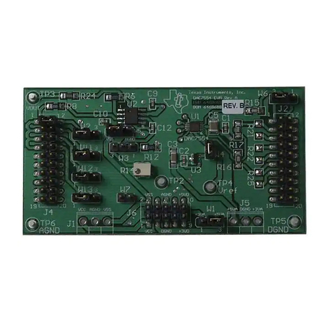
The daughter card has the following I/O connectors/devices:
J1 SMA connector for RF (single-ended or non-inverting differential) input
J2 Base board connector (not visible when the base board and daughter card are mated)
J3 SMA connector for RF(inverting differential) input
The EVB consists of various subsystems that are explained in greater detail in the following sections.
3.1. Si4700/01 Base Board
3.1.1. Microcontroller and Associated Peripherals
The Si4700/01 evaluation environment uses a Silicon Laboratories' C8051F320 microcontroller to control the
Si4700/01 and to provide USB connectivity to the EVB (via J1). The LED D1 illuminates to confirm that power is
being properly supplied to the C8051F320 and firmware has loaded. Push-button PB1 manually resets the
C8051F320. The JTAG connector J2 is used to program the C8051F320 at production time, and is not necessary
for further development.
3.1.2. Reference Clock for the Si4700/01
The Si4700/01 accepts a 32.768 kHz reference clock input at the RCLK pin. On the EVB, this clock is provided by
a precision crystal oscillator. The output of the oscillator is routed to the Si4700/01 RCLK pin through a Schmitt-
trigger buffer (U5) and a 33 Ωseries termination resistor (R19). The user has the option of not using the oscillator
and bringing in the reference clock from an external source through J6. This can be achieved by depopulating R19
and populating R20 with a 0 Ωresistor. Note that the reference clock is not routed through the Schmitt-trigger
buffer when an external clock source is being used.
3.1.3. Power supply network
The EVB accepts three 5 to 7 V power supplies through the power input terminal block J4. Instructions on
connecting the power input terminal can be found in "5. Hardware Setup" on page 7.
The supply labeled VMCU/VIO is the input to regulator U2. The 3.3 V output of the regulator is used to power the
microcontroller and the reference clock systems and also applied to the VIO pin of the Si4700/01. U2 may be
bypassed by depopulating U2 and populating R30 with a 0 Ωresistor. In such a case, the VMCU/VIO supply at J4
must lie between 3.0 and 3.6 V—this condition is necessary to ensure reliable operation of the C8051F320.
The supply label VAUDIO is the input to regulator U6. The 3.3 V output of U6 is used to power the audio amplifier
network.
The supply labeled VRADIO is the input to the regulator U3. The 3.3 V output of the regulator is applied to the VA
and VD pins of the Si4700/01. U3 may be bypassed by depopulating R14 and populating R25 with a 0 Ωresistor.
In such a case, the VRADIO supply at J4 must lie between 2.7 and 5.5 V—these are the recommended operating
conditions for the Si4700/01.
3.1.4. Expansion I/O connector
The 20-pin Expansion I/O connector J3 provides access to all the control signals of the Si4700/01 including the
general purpose input/output pins. Pins for the VA, VD, VIO, and RCLK pins of the Si4700/01 are also available. All
test points on J3 are labeled indicating the signal available at the pin.
Note: The unlabeled pins on J3 between (a) SCLK and RST, and (b) RCLK and GPIO1, provide access to the
system ground.
3.2. Si4700/01 Daughter Card
3.2.1. Si4700/01 FM Tuner Chip
The Si4700/01 (U1) and its bypass capacitors are located on the daughter card. The daughter card allows for the
implementation of different RF input networks to connect the FM inputs at J1 and J3 to the FMIP and FMIN pins of
the Si4700/01 respectively. On the EVB, the Si4700/01 is configured to accept a single-ended FM input—the FMIN
pin is grounded and the FMIP pin is connected to J1 through an ac-coupling capacitor. Refer to “AN231: Si4700/01
Headphone and Antenna Interface” for more information.


