SOYO 5XAE5 Use and care manual

5XAE5
P54C/P55CPCIMainboard
User’sGuide&
TechnicalReference

SOYO
TM
AboutThisGuide
ThisUser’sGuideisforassisting systemmanufacturersand end usersinsetting
upand installing themainboard.Information inthisguidehasbeencarefully
checkedforreliability;however,no guarantee isgivenastothecorrectness of
thecontents.Theinformation inthisdocumentissubjecttochangewithout
notice.
CopyrightNotice
Copyright1997,Soyo ComputerInc.All rightsreserved.Thismanualis
copyrightedby Soyo ComputerInc.Youmaynotreproduce,transmit,transcribe,
storeinaretrievalsystem,ortranslateintoany language,inany formorby any
means,electronic,mechanical,magnetic,optical,chemical,manual,orotherwise,
any partofthispublication withoutexpress writtenpermission ofSoyo Computer
Inc.
Trademarks
Soyo isaregisteredtrademarkofSoyo ComputerInc.All trademarksarethe
propertyoftheirowners.
Disclaimer
Soyo ComputerInc.makesno representationsorwarrantiesregarding the
contentsofthismanual.Wereservetherighttorevisethemanualormake
changesinthespecificationsoftheproductdescribedwithinit atany time
withoutnotice and withoutobligation tonotifyany person ofsuchrevision or
change.Theinformation containedinthismanualisprovidedforgeneraluseby
ourcustomers.Ourcustomersshouldbeawarethatthepersonalcomputerfieldis
thesubjectofmany patents.Ourcustomersshouldensurethattheytake
appropriateaction sothattheiruseofourproductsdoesnotinfringeupon any
patents.ItisthepolicyofSoyo ComputerInc.torespectthevalidpatentrightsof
thirdpartiesand nottoinfringeupon orassistotherstoinfringeupon suchrights.
Restricted RightsLegend
Use,duplication,ordisclosureby theGovernmentissubjecttorestrictionsset
forthinsubparagraph (c)(1)(ii)oftheRightsinTechnicalDataand Computer
Softwareclauseat252.277-7013.
ProductRights
Productmentionedinthismanualarementionedforidentification purposeonly.
Productnamesappearing inthismanualmayormaynotberegisteredtrademarks
orcopyrightsoftheirrespectivecompanies.
Ifyouneedany furtherinformation,pleasecometoourhomepageon internet.
Theaddress is“http://ww.soyo.com.tw”.

Table of Contents
Chapter 1: Introduction .....................................................1
Key Features .................................................................................1
Unpacking the Mainboard.............................................................2
Electrostatic Discharge Precautions..............................................2
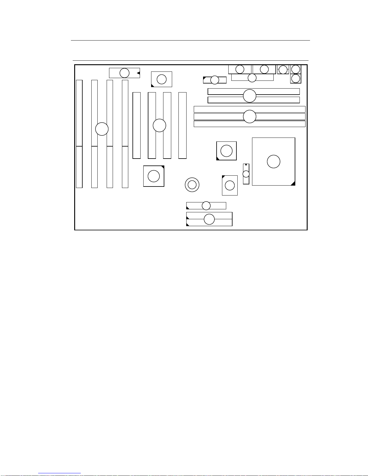
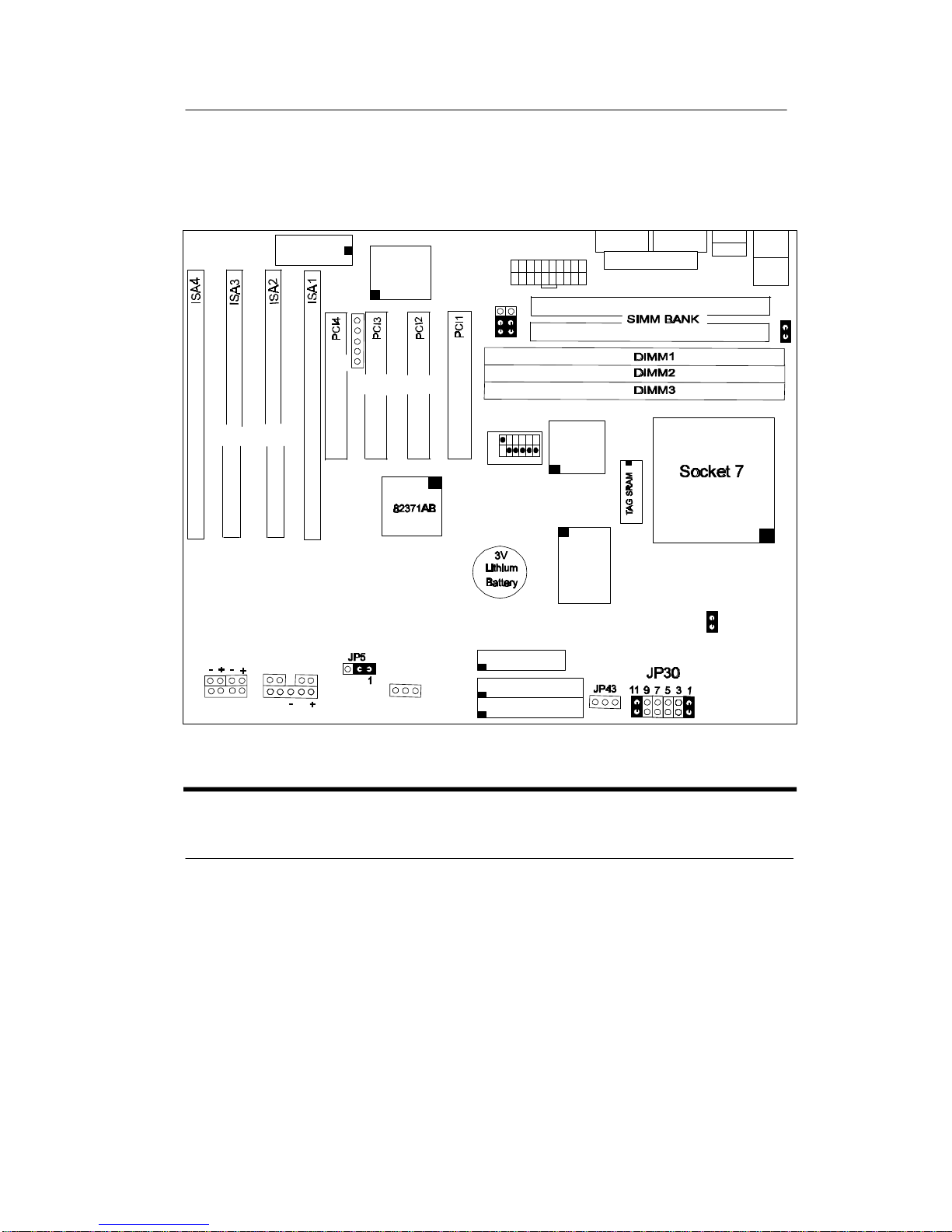
Mainboard Layout w/ Default Settings .........................................3
Chapter 2: Hardware Setup ..............................................5
Jumpers .........................................................................................5
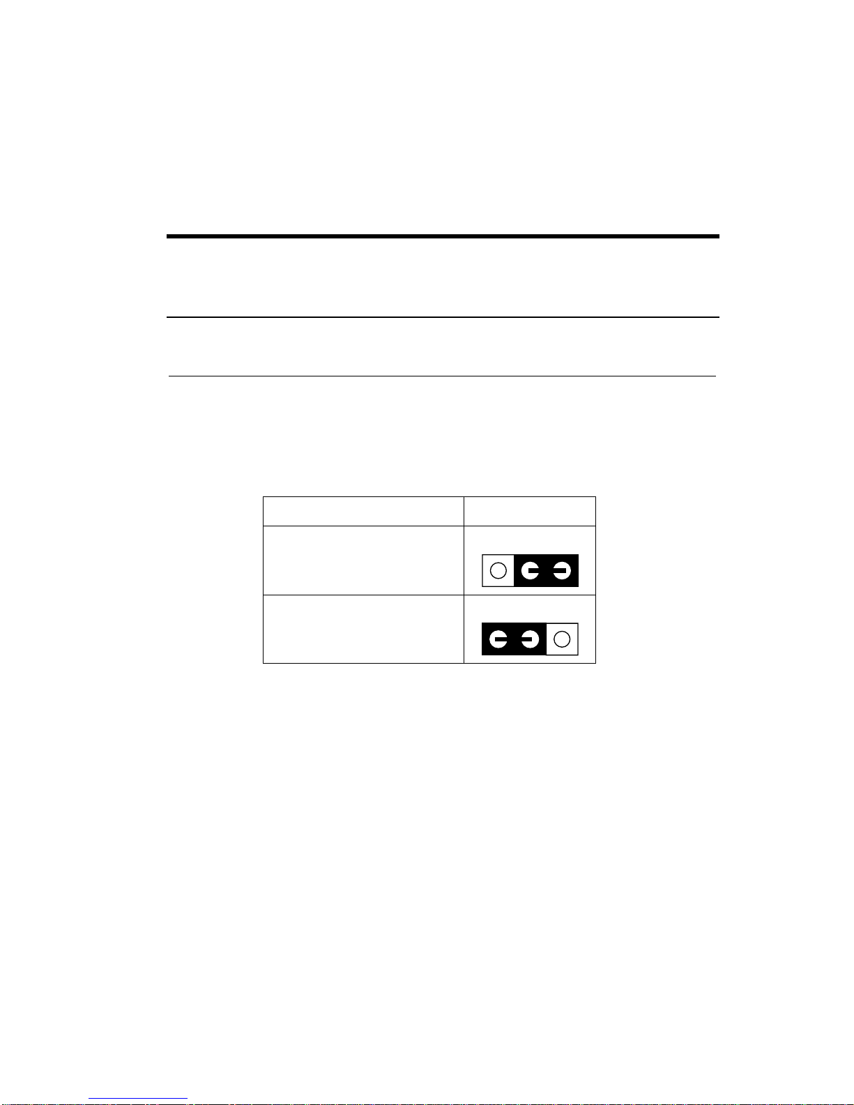
JP5: CMOS Clear Jumper .......................................................5
JP40: CE Test Jumper Pin ......................................................5
JP2: Smart Detect CPU Voltage Function Auto/Manual
Jumper .....................................................................................6
JP37: DIMM Voltage Select Jumper .....................................6
CPU Type Configuration ..............................................................7
Step 1: Frequency Setting.......................................................7
P54C/P55C Ð 75/90/100 CPU Settings (1.5 x clock) .........7
P54C/P55C Ð 100/120/133 CPU Settings (2.0 x clock) .....8
P54C/P55CÐ 150/166 CPU Settings (2.5 x clock) .............9
P54C/P55C Ð 180/200 CPU Settings (3.0 x clock) ..........10
P54C/P55C Ð 233 CPU Settings (3.5 x clock) .................11
AMD K6 Ð PR266 CPU Setting (4.0 x clock)..................12
AMD K6 Ð PR300 CPU Setting (4.5 x Clock) .................12
Step 2: CPU Single/Dual Voltage Setting............................14
Single Voltage CPU Setting .............................................14
Dual Voltage CPU Setting................................................15
Memory Configuration ...............................................................15
Memory Configuration Table................................................16
RAM Bank Installation Notice..............................................16
Cache Configuration ...................................................................16
Cache Size and RAM Locations ...........................................16
Multi I/O Port Addresses ............................................................17
Connectors ..................................................................................17
PW2 Ñ ATX Power Supply On/Off Switch Connector
(Momentary Type).................................................................17
COM1, COM2 Ñ COM1/COM2 Connectors ......................17
JP43: CPU Cooling Fan Connector......................................18
FDC Ñ FDC Connector........................................................18
ATX PW Ñ ATX Power Supply Connectors .......................18
RESET Ð Hardware Reset Control ........................................19
HDD LED Ð HDD LED Connector.......................................19

IDE1/IDE2-OnboardPrimary/SecondaryIDEHDD
Connector…………………………………………………….18
IR1-IRConnector………….……….………………………18
Keylock&PWLED-KeylockandPowerLEDConnector...18
PS/2KBConn.-PS/2KeyboardConnector…………….…..18
PS/2MouseConn.-PS/2MouseConnector……….…….….19
PRT-ParallelPortConnector……………….…..……….….19
SPK-SpeakerConnector…………………….….……….….19
USB1/USB1-UniversalSerialBusConnectors…….…….….19
JP44 -Wake-On-Lan(WOL)Header……..…..…....….….19
Chapter 3:BIOSSetup……………………………………………..20
StandardCMOSSetup……………………………………..…..21
BIOSFeaturesSetup……………………….……………….….23
ChipsetFeaturesSetup…………………….…………….……..26
PowerManagementSetup…………………….……………….28
PNP/PCIConfigurationSetup ………………….…………...31
LoadSetup Defaults……………………….………….………..33
LoadBIOSDefaults……………………….………….………..33
IntegratedPeripherals…………………….………….…………34
SupervisorPassword..…………………….………….….…….37
UserPassword…………………………….………….…….…..38
IDEHDD AutoDetection……………….…………….……….39
Appendix:CPUSettingList……………..………..……………..40
NoteforMemory……………..………..……………..43

1Introduction
The82430 TXPCImainboardisahigh-performanceATXform-factor
systemboardthatsupportsP54C/P55CfamilyCPUs.Thismainboardis
fullycompatiblewithindustrystandards,and addsmanytechnical
enhancements.
KeyFeatures
¡E Processorsupported:
ÄSupportsP54C/P55CfamilyCPUsrunningat75~233 MHzspeeds
;Cyrix6x86/6x86L/6x86MXCPUsrunningatPR150~PR200 speeds
;and AMDK5/K6CPUsrunningatPR75~PR233
Ä
SupportsSOCKET 7forupgrade
Ä
SupportsP54C/P55CseriesSMM modeand CPUstopclock
Ä
SupportsMMXtechnologyand SmartDetectCPUVoltagefunction
¡E L2CacheController
Ä
On-board512KpipelineburstSRAMscache
¡E DRAMController
Ä
SupportsFPM/EDO SIMM (symmetrical/asymmetricaladdressing)
Ä
Supports3stripsof168-pinEDO/SDRMUnbufferedDIMM
Ä
Memoryconfigurationsfrom8MBto256MB
¡E BUSController:
ÄCompliantwithPCIspecification2.1
ÄFour32-bit PCIslots(Masters)and fourISAslots.
Ä
SupportsUniversalSerialBus--- USB
¡E PeripheralController:
ÄSystemBIOSbuilt-inNCR810 BIOSand “Plugand Play”function
ÄOnboardPCIMasterIDEcontrollerand floppycontroller
ÄOnboardtwohighspeedUARTS(w/i 16550 FIFO),oneSPP/EPP/ECP
multi-modeparallelport,and onePS/2mouseport
Ä
OnboardFLASHMemoryforeasyupgradesBIOS
Ä
EasyinstallationofTrionesE-IDE/ATAPICD-ROMBusMaster
Driversincluded
ÄOnboardIRfunction.

2Introduction
Unpacking the Mainboard
The mainboard package contains:
¥ The 82430TX Mainboard
¥ This UserÕs Guide
¥ One IDE Bus Master driver diskette
Note: Do not unpack the mainboard until you are ready to install it.
Follow the precautions below while unpacking the mainboard.
1. Before handling the mainboard, ground yourself by grasping an
unpainted portion of the systemÕs metal chassis.
2. Remove the mainboard from its anti-static packaging and place it on
a grounded surface, component side up.
3. Check the mainboard for damage. If any chip appears loose, press
carefully to seat it firmly in its socket.
Do not apply power if the mainboard appears damaged. If there is
damage to the board contact your dealer immediately.
Electrostatic Discharge Precautions
Make sure you ground yourself before handling the mainboard or other
system components. Electrostatic discharge can easily damage the
components. Note that you must take special precaution when handling
the mainboard in dry or air-conditioned environments.
Take these precautions to protect your equipment from electrostatic
discharge:
¥ Do not remove the anti-static packaging until you are ready to install
the mainboard and other system components.
¥ Ground yourself before removing any system component from its
protective anti-static packaging. To ground yourself grasp the
expansion slot covers or other unpainted portions of the computer
chassis.
¥ Frequently ground yourself while working, or use a grounding strap.
¥ Handle the mainboard by the edges and avoid touching its
components.

Introduction 3
Mainboard Layout w/ Default Settings
1
2
2
3
9
10
4
12
14 14
15 13
6
11
18 17
16
78
5
19
Figure 1Ð1. Mainboard Layout
1. ZIF socket 7 (for P54C/P55C) 11. Floppy Connector
2. 82430 TX Chipset 12. IDE1/IDE2 Connector
3. Pipelined Burst SRAM 13. Parallel Port Connector
4. Ultra I/O Chip 14. COM1/COM2 Connector
5. PnP FLASH BIOS 15. ATX Power Supply
Connector
6. TAG SRAM 16. PS/2 Mouse Connector
7. ISA Slots 17. PS/2 KB Connector
8. PCI Slots 18. USB port connectors
9.
10.
SIMM Bank
Unbuffered DIMM Bank
19. Lithium battery (for
CMOS memory, 3V)

JP40
1JP37
ISA Slots
PCISlots
W83977F
FLASHBIOSUSB1
USB2
COM1
COM2
3
5
PS/2
KB Con
PS/2
Mouse
3 1
82439TX
(for586 CPUFamily)
W25P240AF
(512 Cache)
HDD LEDTBLEDPWRESET
KEY
LOCKPWLED
SPK 1
JP2
JP44
1
FDC
IDE2
IDE1
PRT
ATX PWCon.
1
Figure1-2.MainboardDefault Setting
Important:Makesurethesystem iswell ventilatedto prevent
overheating andensuresystemstability.
4Introduction
Default settingsareasfollows:P54C/P55C133MHzCPU,512KPipe-
linedBurstcache,On-boardPCIE- IDE Enabled,2highspeedUA-
RTSEnabled(w/16550 FIFO),1EPP/ECPport(ECP+EPP mode),5V
DRAM/3.3V DIMM,andATXpowersupply.
IR1
1
5
1
1 2 3 4 5 6
ONSW1

2 Hardware Setup
This chapter explains how to configure the mainboardÕs hardware. After
you install the mainboard, you can set jumpers, install memory on the
mainboard, and make case connections. Refer to this chapter whenever
you upgrade or reconfigure your system.
CAUTION:Turn off power to the mainboard, system chassis, and
peripheral devices before performing any work on the
mainboard or system.
Jumpers
JP5: CMOS Clear Jumper
Clear the CMOS memory by momentarily shorting pin 2Ð3; then
shorting pin 1Ð2 to retain new settings.
CMOS Setting JP5
Retain CMOS data
(default)
1
Clear CMOS data
1
JP40: CE Test Jumper Pin
This connector is reserved for the CE test. If you run into problems
during the CE test, unplug the jumper pin and try again.

6Hareware Setup
JP2: Smart Detect CPU Voltage Function Auto/Manual
Jumper
This jumper is reserved for few old non-Intel CPUs which can not be
detected correctly. If you run into problems while detecting the voltage
of old non-Intel CPUs, remove this jumper to correct it.
JP37: DIMM Voltage Select Jumper
Most of DIMMs in the consumer market is still 3.3V and this jumper is
reserved only for upgrading purpose in the near feature. If you have 5V
SIMM or DIMM which matches the existing 3.3V DIMM socket on this
mainboard, than you need to set this jumper to 5V before installing the
SIMM or DIMM.
DIMM Voltage JP37
3.3V (default)
1
5V
1
Caution: Do not change this jumper to 5V setting unless you are sure
that your DIMMs are 5V. The wrong setting may cause the
system malfunction.

Hareware Setup 7
CPU Type Configuration
This section shows you how to configure your CPU step by step. Note
that you need to check the CPU voltage before installation. This board
supports the Intel P54C/P55C/MMX, Cyrix 6x86/6x86L/6x86MX, and
AMD 5K86/K5/K6 CPUs. With the MMX technology supported, you
should be able to use MMX CPUs and configure these CPUs as normal
dual voltage CPUs.
❑Step 1: Frequency Setting
P54C/P55C – 75/90/100 CPU Settings (1.5 x clock)
AMD K5 – PR75/PR90/PR100/PR120/PR133 (1.5 x clock)
654321
ON
SW1
654321
ON
SW1
654321
ON
SW1
W25P240AF
82439TX
SW1
654231
ON
Lithium
Battery
P54C/P55C– 90/60 MHz
AMD K5 – PR 90/60MHz
AMD K5 – PR 120/60 MHz
P54C/P55C– 100/66 MHz
AMD K5 – PR 100/66 MHz
AMD K5 – PR 133/66 MHz
P54C/P55C– 75/50 MHz
AMD K5 – PR 75/50 MHz
Figure 2Ð1Ð1. CPU Jumper Settings
Note: 1. You must equip the CPU with a fan and heat sink for system
stability.
2. AMD K5ÐPR90= AMD 5k86(SSA5)ÐP90.

Figure2-1-2.CPUJumperSettings
Note:1.You mustequiptheCPUwith a fan and heatsinkfor system
stability.
P54C/P55C-100/50 MHz
Cyrix 6x86/6x86L-PR200+/75MHz
Pentium-133/66 MHz
Cyrix 6x86/6x86L-PR166+/66 MHz
P54C/P55C-120/60 MHz
Cyrix 6x86/6x86L-PR150+/60 MHz
AMDK5/K6-PR150
8HardwareSetup
82439TX
W25P240AF
Lithium
Battery
2.Thehostbusfrequency ofCyrix6x86L-PR200+CPUisover
thestandardvalue,therefore,you needto usehigher
standard devicestomeet thespecificationsofsuchCPUs.
(ie., high qualityDRAM/VGAcard.)

Hareware Setup 9
P54C/P55C– 150/166 CPU Settings (2.5 x clock)
Cyrix 6x86MX – PR166/PR200/PR233 CPU Settings (2.5 x clock)
AMD K5/K6– PR166 CPU Setting
W25P240AF
82439TX
SW1
654231
ON
Lithium
Battery
P54C/P55C– 166/66 MHz
Cyrix 6x86MX – PR200/66 MHz
AMD K5/K6 – PR 166
Cyrix 6x86MX – PR233/75 MHz
P54C/P55C– 150/60 MHz
Cyrix 6x86MX – PR166/60 MHz
654321
ON
SW1
654321
ON
SW1
654321
ON
SW1
Figure 2Ð1Ð3. CPU Jumper Settings
Note: The host bus frequency of Cyrix 6x86MXÐPR233+CPU is over
the standard value, therefore, you need to use higher standard
devices to meet the specifications of such CPUs, (i.e., high
quality DRAM/VGA card.)

10 Hareware Setup
P54C/P55C – 180/200 CPU Settings (3.0 x clock)
Cyrix 6x86MX – PR233/PR266 CPU Settings (3.0 x clock)
AMD K6 – PR200 CPU Setting
W25P240AF
82439TX
SW1
654231
ON
Lithium
Battery
P54C/P55C– 200/66 MHz
AMD-K6/PR2-200
Cyrix 6x86MX – PR233/66MHz
Cyrix 6x86MX – PR266/75 MHz
P54C/P55C– 180/60 MHz
654321
ON
SW1
654321
ON
SW1
654321
ON
SW1
Figure 2Ð1Ð4. CPU Jumper Settings
Note: 1. You must equip the CPU with a fan and heat sink for system
stability.
2. The host bus frequency of Cyrix 6x86MXÐPR266 CPU is over
the standard value, therefore, you need to use higher
standard devices to meet the specifications of such CPUs,
(i.e., high quality DRAM/VGA card.)

Hareware Setup 11
P54C/P55C – 233 CPU Settings (3.5 x clock)
Cyrix 6x86MX – PR266 Cpu Setting (3.5 x clock)
AMD K6 – PR233 CPU Setting
W25P240AF
82439TX
Lithium
Battery
Socket 7
(for 586 CPU Family)
654321
ON
SW1
Figure 2Ð1Ð5. CPU Jumper Settings
Note: The host bus frequency of Cyrix 6x86MXÐPR266 CPU is over
the standard value, therefore, you need to use higher standard
devices to meet the specifications of such CPUs, (i.e., high
quality DRAM/VGA card.)

12 Hareware Setup
AMD K6 – PR266 CPU Setting (4.0 x clock)
W25P240AF
82439TX
Lithium
Battery
Socket 7
(for 586 CPU Family)
654321
ON
SW1
Figure 2Ð1Ð6. CPU Jumper Settings
AMD K6 – PR300 CPU Setting (4.5 x Clock)
W25P240AF
82439TX
Lithium
Battery
Socket 7
(for 586 CPU Family)
654321
ON
SW1
Figure 2Ð1Ð7. CPU Jumper Settings
Note: You must equip the CPU with a fan and heat sink for system
stability.

Hareware Setup 13
❑Step 2: CPU Single/Dual Voltage Setting
There are two kinds of CPU input voltages due to various designs of
CPUsÑsingle voltage and dual voltage. Set your CPU according to the
type that you have.
For Intel P54C/P55C single and dual voltage series CPUs, there is no
need to adjust any jumper for CPU voltag due to the Smart Detect CPU
Voltage function.
Single Voltage CPU Setting
Signal voltage CPUs use the same voltage for VIO and VCore and has
been used traditionally. The CPUs which fall into this category are Intel
P54C series, AMD-K5-PRxxxBx, AMD-K5-PRxxxCx, AMD-K5-
PRxxxFx, and Cyrix 6x86. Refer to the following figures to set these
CPUsÕ voltage:
Socket 7
(for 586 CPU Family)
W25P240AF
IDE1
IDE2
FDC
JP30
11 13579
JP30
11 13579
3.3V CPU (i.e., P54C)
JP30
11 13579
3.52V CPU(default)
(i.e., P54C/6x86/K5)
Figure 2Ð2Ð1. Single Voltage CPU
Note: Please ask your CPU dealer for the exact CPU voltage before
you install it.

14 Hareware Setup
Dual Voltage CPU Setting
Dual voltage CPUs are designed to use different voltage for VIO and
VCore and they include Intel P55C series, Cyrix 6x86L/MX, AMD K6,
and MMX technology included CPUs. Refer to the following figures to
set these CPUsÕ voltage:
Socket 7
(for 586 CPU Family)
W25P240AF
IDE1
IDE2
FDC
JP30
11 13579
JP30
11 13579
2.1V CPU
(i.e., K6)
JP30
11 13579
2.9V CPU
(i.e., K6)
JP30
11 13579
3.2V CPU
(i.e., K6)
JP30
11 13579
2.8V CPU (default)
(i.e., P55C, 6x86L/MX)
Figure 2Ð2Ð2. Dual Voltage CPU
Note: Due to various design, please ask your CPU dealer for the exact
VIO and VCORE voltage before you install it.
Memory Configuration
The mainboard supports two banks of 72-pin SIMM modules and three
strips of 168-pin/3.3V Unbuffered DIMM modules. The mainboard
requires SIMM of at least 70ns access time.
The mainboard supports from 4 to 256 Mbytes with no other restrictions
on memory configurations. You must install two strips of SIMM
modules to complete a bank.

Hareware Setup 15
Memory Configuration Table
SIMM Bank DIMM Bank
Bank 0 DIMM 1 DIMM 2 DIMM 3
RAM Type FPM/EDO FPM/EDO
SDRAM
FPM/EDO/
SDRAM
FPM/EDO/
SDRAM
Single
RAM
Module
Size (MB)
4/8/16/32/64 8/16/32/64 8/16/32/64 8/16/32/64
Note: Do not install FPM or EDO SIMM/DIMM when you already
installed SDRAM type of DIMM.
RAM Bank Installation Notice
Due to the RAS line share architecture of TX chipset, do not install
SIMM bank with DIMM3. All other combinations are acceptable.
Cache Configuration
The mainboard has a write-back caching scheme with built-in 512KB
Level 2 Pipelined Burst cache onboard to improve the system
performance.
Cache Size and RAM Locations
Cache Size Cache RAM TAG RAM Cacheable
Range
512KB 64K x 64
on U5
16K x 8
on U4
64 MB

16 Hardware
Setup
MultiI/O PortAddresses
Default settingsformulti I/Oportaddressesareshowninthetable
below.
PortI/OAddress IRQStatus
LPT1*
378H7ECP+EPP
COM1
3F8H4
COM2
2F8H3
*If default I/OportaddressesconflictwithotherI/Ocard(e.g.sound
cardsorI/Ocards),you mustadjustoneoftheI/Oaddressestoavoid
address conflict.(You canadjusttheseI/OaddressesfromtheBIOS
setup.)
Note:Somesound cardshaveadefault IRQsetting forIRQ7,whichmay
conflictwithprinting functions.If thisoccursdo notusesound card
functionsatthesametimeyou print.
Connectors
Attachthemainboardtocasedevicesviaconnectorson themainboard.
RefertoFigure1-1forconnectorlocationsand connectorpinpositions.
PW–ATXPowerSupplyOn/Off SwitchConnector
(Momentarytype)
Attachatwo-pinswitchtothisconnectorforturning theATXpower
supplyon/off.
COM1,COM2–COM1/COM2Connectors
AttachCOM1/COM2device totheseconnectors.
This manual suits for next models
2
Table of contents
Other SOYO Motherboard manuals

SOYO
SOYO SY-5EMA+ User manual

SOYO
SOYO SY-5EH5 Use and care manual

SOYO
SOYO SY-7VEM User manual

SOYO
SOYO SY-6IEB User manual

SOYO
SOYO SY-7IWM User manual

SOYO
SOYO SC-5EA5 Quick start guide

SOYO
SOYO SY-P4VTE User manual

SOYO
SOYO SY-P4ISR User manual

SOYO
SOYO TechAID User manual

SOYO
SOYO Super 7 V1.0 User manual

SOYO
SOYO Pentium SiS 551x Use and care manual

SOYO
SOYO SY-P4VGA User manual

SOYO
SOYO SY-P4I845PE User manual

SOYO
SOYO SY-D6IBA User manual

SOYO
SOYO SY-P4VDA User manual

SOYO
SOYO SY-6BA+ User manual

SOYO
SOYO SY-K7VLM-B User manual

SOYO
SOYO SY-7IZM Use and care manual

SOYO
SOYO 6KB Use and care manual

SOYO
SOYO SY-6ZE+ Use and care manual