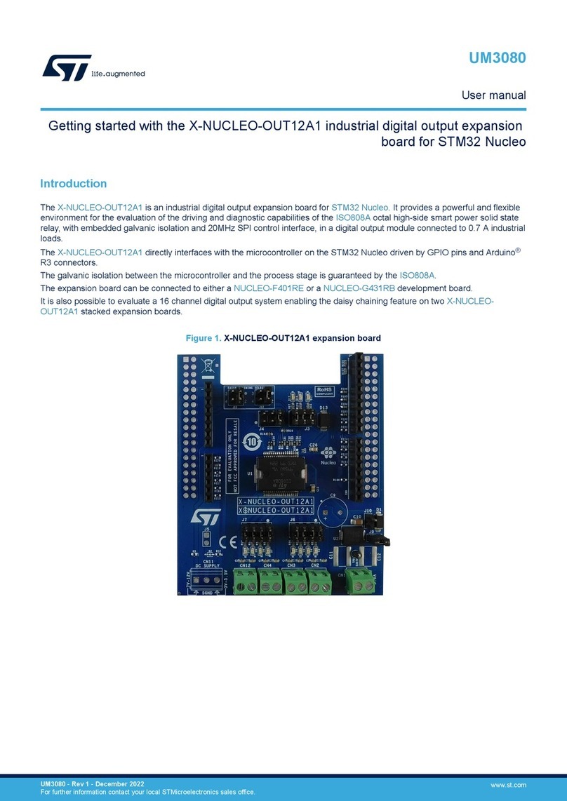
ST UM2727 User manual

Introduction
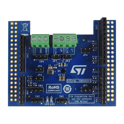
The X-NUCLEO-OUT03A1 industrial digital output expansion board for STM32 Nucleo provides a powerful and flexible
environment for the evaluation of the driving and diagnostic capabilities of the IPS2050H (dual high-side smart power solid
state relay) in a digital output module connected to 2.5 A (max.) industrial loads.
The X-NUCLEO-OUT03A1 interfaces with the microcontroller on the STM32 Nucleo via 5 kV optocouplers driven by GPIO
pins, Arduino UNO R3 (default configuration) and ST morpho (optional, not mounted) connectors.
The expansion board can be connected to either a NUCLEO-F401RE or NUCLEO-G431RB development board.
It is also possible to evaluate a system composed by up to four stacked X-NUCLEO-OUT03A1 expansion boards.
As an example, a system with four X-NUCLEO-OUT03A1 expansion boards allows you to evaluate an eight-channel digital
output module with 2.5 A (max.) capability each.
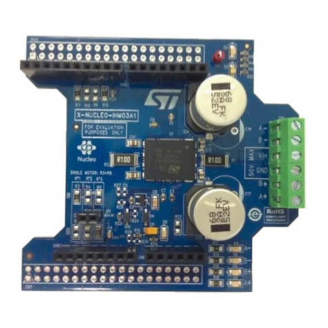
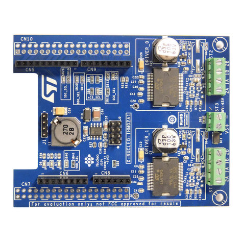
Figure 1. X-NUCLEO-OUT03A1 expansion board
RELATED LINKS
For further details on configuration resistors, refer to UM2863
Getting started with X-NUCLEO-OUT03A1 industrial digital output expansion
board for STM32 Nucleo
UM2727
User manual
UM2727 - Rev 1 - August 2021
For further information contact your local STMicroelectronics sales office.
www.st.com

1Getting started
1.1 Overview
The X-NUCLEO-OUT03A1 embeds the IPS2050H intelligent power switch (IPS), featuring overcurrent and
overtemperature protection for safe output load control.
The board is designed to meet application requirements in terms of galvanic isolation between user and power
interfaces. This requirement is satisfied by optical isolation implemented through four optocouplers (ISO1, ISO2,
ISO3 and ISO4) for signal forward to the device and FLT pins for feedback diagnostic signals.
• Based on IPS2050H dual high-side switch, which features:
– Operating range up to 60 V/2.5 A
– Low power dissipation (RON(MAX) = 50 mΩ)
– Fast decay for inductive loads
– Smart driving of capacitive load
– Under-voltage lock-out
– Per-channel overload and over-temperature protection
– PSSO24 package
• Application board operating range: 8 to 33 V/0 to 2.5 A
• Extended voltage operating range (J3 open) up to 60 V
• Green LEDs for output on/off status
• Red LEDs for per-channel diagnostic (overload and overheating)
• 5 kV galvanic isolation
• Supply rail reverse polarity protection
• EMC compliance with IEC61000-4-2, IEC61000-4-3, IEC61000-4-5
• Compatible with STM32 Nucleo development boards
• Equipped with Arduino UNO R3 connectors
• CE certified
• RoHS and China RoHS compliant
UM2727
Getting started
UM2727 - Rev 1 page 2/15

1.1.1 Digital section
The digital section is associated with the STM32 interface and digital supply voltage to and from the X-NUCLEO-
OUT03A1 expansion board.
Figure 2. X-NUCLEO-OUT03A1 expansion board: digital interface components
The four Arduino UNO R3 connectors:
•allow expansion board communication with the STM32 Nucleo development board microcontroller accessing
STM32 peripheral and GPIO resources;
• provide digital supply voltage between the STM32 Nucleo development board and the X-NUCLEO-
OUT03A1 expansion board, in either direction.
Normally, the STM32 Nucleo development board supplies the expansion board by a 3v3 or 5v0 generated by the
USB. You can select the preferred voltage on the expansion board via SW3 (3v3 closing pins 1-2; 5v0 closing
pins 2-3).
Alternatively, it is possible to supply the STM32 Nucleo development board by the expansion board. In this
case, an external supply voltage (7-12 V) should be connected CN2 connector (not mounted by default) on the
expansion board and the ground loop should be closed by mounting D2 (enable the reverse polarity protection) or
by closing J17 (without reverse polarity).
To supply the VIN voltage rail is necessary to:
• close jumper JP5 between pins 2 and 3 and open jumper JP1 on the NUCLEO-F401RE
• open jumper JP5 between pins 1 and 2 and close jumper JP5 between pins 3 and 4 on the NUCLEO-
G431RB
UM2727
Overview
UM2727 - Rev 1 page 3/15

1.1.2 Power section
The power section involves the power supply voltage (CN1, pin 2 and 3 for VCC, pin 4 for GND), load connection
(between CN1 pins 1-4 and CN1 pins 5-4) and electromagnetic compatibility (EMC) protection.
Figure 3. X-NUCLEO-OUT03A1 expansion board: power stage components
1. Output channel 1 - fault red LED
2. Output channel 2 - fault red LED
3. Output channel 1 - green LED
4. Output channel 2 - green LED
5. IPS2050H
6. Output and power supply connector
1
2
5
3
4
6
For EMC:
• The SM15T39CA transient voltage suppressor (TR1), enabled by closing JP3, is placed between VCC and
GND tracks to protect the IPS2050H against surge discharge on the supply rail path up to ±1kV/2Ω coupling;
• in common mode surge testing, two single-layer capacitors (C1 and C2 - not included) must be soldered at
the predisposed locations;
• the IPS2050H output stages do not require additional EMC protections with respect to the IEC61000-4-2,
IEC61000-4-3, IEC61000-4-5 standards.
UM2727
Overview
UM2727 - Rev 1 page 4/15

1.2 Hardware requirements
The X-NUCLEO-OUT03A1 expansion board is designed to be used with the NUCLEO-F401RE or NUCLEO-
G431RB STM32 Nucleo development boards.
To function correctly, the X-NUCLEO-OUT03A1 must be plugged onto the matching Arduino UNO R3 connector
pins on the STM32 Nucleo board as shown below.
Figure 4. X-NUCLEO-OUT03A1 and STM32 Nucleo stack
1.3 System requirements
To use the STM32 Nucleo development boards with the X-NUCLEO-OUT03A1 expansion board, you need:
• a Windows PC/laptop (Windows 7 or above)
• a type A to mini-B USB cable to connect the STM32 Nucleo board to the PC when using a NUCLEO-
F401RE development board
• a type A to micro-B USB cable to connect the STM32 Nucleo board to the PC when using a NUCLEO-
G431RB development board
• the X-CUBE-OUT3 firmware and software package installed on your PC/laptop
1.4 Board setup
Step 1. Connect the micro-USB or mini/USB cable to your PC to use the X-NUCLEO-OUT03A1 with NUCLEO-
F401RE or NUCLEO-G431RB development board
UM2727
Hardware requirements
UM2727 - Rev 1 page 5/15

Step 2. Download the firmware (.bin or .hex) onto the STM32 Nucleo development board microcontroller
through STM32 ST-LINK utility, STM32CubeProgrammer and according to your IDE environment as
detailed in the table below.
Table 1. NUCLEO-F401RE development board supported IDEs - bin files
NUCLEO-F401RE
IAR Keil STM32CubeIDE
EWARM-OUT03_04-
STM32F4xx_Nucleo.bin
MDK-ARM-OUT03_04-
STM32F4xx_Nucleo.bin
STM32CubeIDE-OUT03_04-
STM32F4xx_Nucleo.bin
Table 2. NUCLEO-G431RB development board supported IDEs - bin files
NUCLEO-G431RB
IAR Keil STM32CubeIDE
EWARM-OUT03_04-
STM32G4xx_Nucleo.bin
MDK-ARM-OUT03_04-
STM32G4xx_Nucleo.bin
STM32CubeIDE-OUT03_04-
STM32G4xx_Nucleo.bin
Step 3. Connect the IPS2050H device supply voltage via CN1 (see Section 1.1.2 Power section).
Step 4. Provide the digital supply voltage (see Section 1.1.1 Digital section).
Step 5. Connect the load on the output connector (see Section 1.1.2 Power section).
Step 6. Reset the example sequence by pushing the black button on the STM32 Nucleo board.
Step 7. Push the blue button on STM32 Nucleo board to choose among the examples provided in the default
firmware package.
1.5 Multiple board configuration
It is also possible to evaluate an eight channel digital output module by stacking four X-NUCLEO-OUT03A1 with
shared or independent supply rail and independent loads.
In this case, the four expansion boards (board 0, 1, 2, 3 as shown in the table below) must be properly configured:
for board 1, 2 and 3, it is necessary to unsolder four resistors for each board from the default position and solder
them back in the alternate positions according to the following table.
Table 3. Configuration of a stack of four expansion boards
Board no. IN1 IN2 FLT1 FLT2
Board 0 R101 R102 R103 R104
Board 1 R131 R132 R133 R134
Board 2 R111 R112 R113 R114
Board 3 R121 R122 R123 R124
Important:
When using Board 2 and Board 3, two jumpers must close the morpho connectors pins in the STM32 Nucleo board:
• CN7.35-36 closed
• CN10.25-26 closed
UM2727
Multiple board configuration
UM2727 - Rev 1 page 6/15

2Schematic diagrams
Figure 5. X-NUCLEO-OUT03A1 circuit schematic (1 of 2)
3
R134100R N.M.
5
6
36
1
IN1
R131100R N.M.
15
VCC
2
IN1
16
A4
ALTERNATE USE
D8
ST morpho connectors (N.M.)
D3
23
R102100R
PB5
J3
ALTERNATE USE
ALTERNATE USE
ALTERNATE USE
ALTERNATE USE
16
D9
36
D5
7
C6
2.2uF/100V
37
2
22
R133100R N.M.
27
R123100R N.M.
TR2
ESDA15P60-1U1M (N.M.)
PA6
PA8
J4
VCC
4
20
NRST
31
R121100R N.M.
2
PA2
PB9
D0
ALTERNATE USE
D2
BAT48JFILM (N.M.)
2
18 17
23
D10
10
28
D12
SM15T39CA
10
IN1
TR1
FLT2
1
12
CN1
CON5
IN2
38
19
R104100R
ALTERNATE USE
4
CN9
3
PC1
PA7
GND
FLT1
DEFAULT
IN1
15
IN1
OUT2
A3
1
R114100R N.M.
2 1
VIN
5
IOREF
R113100R N.M.
CN2
CON2 (N.M.)
6
8
CN5
D1STPS1H100A
ALTERNATE USE
25
1
PB6
PB0
PB4
3
32
34
default open
2
3
35
3v3
FLT2
4
PA4
FLT1
R112100R N.M. IN2
J17
8
OUT1
24
26
29
12
5
4
34
5
1
7
19
C2
4.7nF/3kV(N.M)
2
9
38
FLT2
DEFAULT
D11
2
25
DEFAULT
ALTERNATE USE
OUT2
FLT1
21
5v0
3
IN2
3
A1
D13
9
4
13
30
26
6
R124100R N.M.
21
1
8
10
R132100R N.M.
A5
1
VIN
35
8
7
default open
(7V-12V NUCLEO supply voltage)
R122100R N.M.
6
D14
3
D7
FLT1
FLT2
4
6
FLT1
7
5V
6
30
D15
IN2
PA3
PA1
PC7
PB10
R103100R
IN2
GND
C13
N.M.(100uF)
1
8
D6
FLT1
1
27
2
2
22
C1
4.7nF/3kV(N.M)
Alternate Nucleo supply
7 V - 12 V
13
31
A2
5
4
DEFAULT
ALTERNATE USE
2
9
7
PB8
ALTERNATE USE
ALTERNATE USE
D1
GND
29
PA10
2
37
OUT1
24
FLT2
FLT2
3V3
CN6
33
CN10
CON38
5
28
IN2
R101100R
14
A0
AVDD
11
1
EARTH
PA9
PC0
PA0
PA5
PB3
32
IN1
D4
VCC
17
1
default open
11
R111100R N.M.
D2
14
5
Analog supply
8 V - 60 V
Arduino connectors
33
20
CN7
CON38
CN8
18
UM2727 - Rev 1 page 7/15
UM2727
Schematic diagrams

Figure 6. X-NUCLEO-OUT03A1 circuit schematic (2 of 2)
OUT1
R132.2k
TP1
C3
100nF/100V
470nF
4
2
21
R15
10k
4
SW4
R722k
IN1
SW1
13
23
R822k
1
1
1
ISO3
TLP383
J2
SW5
C7
0.47nF
18
2
J6
OUT2
1
3
25
TP5
R2
27k
11
SW3
J13
J12
C4
100nF/100V
8
4
7
2
ISO1
TLP383
1
R11
0R
5
J14
4
2
20
DG2GREEN LED
OUT2
IPD1
FLT1
IN1
FLT2
R10
10k
VCC
6
12
2
J1
3
9
6
J8
C9
470nF
C12
0.47nF
C10
6
3
19
default:
closed
default: closed
1
2
3
default:
CLOSE 1-2
13
2
default:
CLOSE 1-2
R4
22k
ISO4
TLP383
6
5
10
IN2
1
R1
27k
ISO2
TLP383
2
R16
0R
1
J11
22
R6
390
4
1
1
5v0
1
6
2
J10
5
R17
0R
RED LED
SW2
2
TP3
IPD2
default:
closed
default: open
OUT1
R9
10k
2
C11
47nF
16
FLT2
R14
10k
2
1
1
J7
DR1
2
6
1
1 2
IN2
3
default: open
default: closed
2
default: closed
1
3
default:
CLOSE 1-2
default: close 1-23
default: closed
1
1
default:
CLOSE 1-2
2
2
IN2
3
TP2
14
TP4
DG1GREEN LED
3v3
47nF
VCC
R182.2k
4
FLT1
1
R3
22k
1
4
RED LED
2
DR2
1
R12
0R
3
15
24
17
C8
3
VCC
3
U1
PSSO24
J5
R5
390
6
J9
C5
100nF/100V
UM2727 - Rev 1 page 8/15
UM2727
Schematic diagrams

3Bill of materials
Table 4. X-NUCLEO-OUT03A1 bill of materials
Item Q.ty Ref. Part / Value Description Manufacturer Order code
1 1 U1 IPS2050H PSSO24
Dual high-side
smart power solid
state relay
ST IPS2050H-TR
2 1 CN1 5 ways, 1 row 24 A TH 5
mm Connector WURTH 691137710005
3 0 C1,C2 4.7 nF 3kV 1825 Connectors (not
mounted) Vishay HV1825Y472KXHATHV
4 1 TR1
1.5 kW
Vbr = 39 V
Vcl = 53.9 V
SMC
1500 W, 33.3 V
TVS in SMC ST SM15T39CA
5 1 D1 1 A, 100 V SMA 100 V, 1 A power
Schottky rectifier ST STPS1H100A
6 11
J1, J2, J3, J4,
J5, J6, J7, J12,
J13, J14 J17
2 ways, 1 row TH 2.54
mm Jumpers WURTH 61300211121
7 0 J10, J11 TH 2.54 mm Jumpers (not
mounted) Any Any
8 3 C3, C4, C5 100 nF 100 V 0805 X7R Capacitors WURTH 885012207128
9 1 C6 2.2 µF 100 V 1206 X7R Capacitor AVX 12061C225KAT2A
10 2 C7, C10 470pF 16V 0603 X7R Capacitors WURTH 885012206032
11 2 C8, C11 47nF 16V 0603 X7R Capacitors WURTH 885012206044
12 2 C9, C12 470nF 25V 0603 X7R Capacitors WURTH 885012206075
13 0 C13 Capacitor (not
mounted) Any Any
14 4 ISO1, ISO2
ISO3, ISO4
VCE = 80V VISO=5kV
11-4P1A Optocouplers
TOSHIBA TLP383
WURTH 140100146000
15 2 R1, R2 27 kΩ 0.1 W 0603 Resistors MULTICOMP MCMR06X2702FTL
16 2 R3, R4 22 kΩ 0.1 W 0603 Resistors VISHAY CRCW060322K0FKEA
17 2 R5, R6 390 Ω 0.1 W 0603 Resistors YAGEO RC0603FR-07390RL
18 2 DG1, DG2 150060GS75000 Green LEDs WURTH 150060GS75000
19 2 R7, R8 22 kΩ 0.2 W 0603 Resistors TE-CONN CRGH0603J22K
20 2 DR1, DR2 150060RS75000 Red LEDs WURTH 150060RS75000
21 2 J8, J9 6 ways, 2 rows connector
SMD 2.54 mm Jumpers WURTH 61030621121
22 4 R9, R10, R14,
R15 10kΩ 0.1W ±1% 0603 Resistors Bourns CR0603-FX-1002ELF
23 4 R11, R12, R16,
R17 0Ω 0.1W 0603 Resistors MULTICOMP MCWR06X000 PTL
24 2 R13, R18 2.2kΩ 0.1W 0603 Resistors MULTICOMP MCMR06X2201FTL
25 4 R101, R102,
R103, R104 100Ω 0.1W ±0.5% 0603 Resistors Panasonic ERJ3BD1000V
UM2727
Bill of materials
UM2727 - Rev 1 page 9/15

Item Q.ty Ref. Part / Value Description Manufacturer Order code
26 0
R111, R121,
R131 R112,
R122, R32 R113,
R123, R133
R114, R124,
R134
603 Resistors (not
mounted) Any Any
27 5 SW1, SW2,
SW3, SW4, SW5
3 ways, 1 row SMD 2.54
mm Connectors TE-CONN 1241150-3
28 1 CN2 2 ways, 1 row TH 5mm Connector WURTH 691137710002
29 0 D2 (DNM) 0.35 A, 40 V SOD-323
General purpose
signal Schottky
diode
ST BAT48JFILM
30 0 TR2
1200 W
Vbr = 6.8 V
Vcl = 10.2 V
1610
High power
transient voltage
suppressor
ST ESDA15P60-1U1M
31 1 CN5 10 ways, 1 row TH 2.54
mm Connector
SAMTEC ESQ-110-14-T-S
4UCON 17896
32 2 CN6, CN9 8 ways, 1 row TH 2.54
mm Connectors
SAMTEC ESQ-108-14-T-S
4UCON 15782
33 1 CN8 6 ways, 1 row TH 2.54
mm Connector
SAMTEC ESQ-106-04-T-S
4UCON 15781
34 0 CN7, CN10 TH 2.54 mm Connectors (not
mounted) SAMTEC ESQ-119-14-T-D
35 5 TP1, TP2, TP3,
TP4, TP5 TH d = 1mm Test points RS 262-2034
36 18 2.54 mm Jumper WURTH 60900213421
UM2727
Bill of materials
UM2727 - Rev 1 page 10/15

Revision history
Table 5. Document revision history
Date Revision Changes
04-Aug-2021 1 Initial release.
UM2727
UM2727 - Rev 1 page 11/15

Contents
1Getting started ....................................................................2
1.1 Overview .....................................................................2
1.1.1 Digital section ...........................................................3
1.1.2 Power section ...........................................................4
1.2 Hardware requirements .........................................................5
1.3 System requirements ...........................................................5
1.4 Board setup ...................................................................5
1.5 Multiple board configuration......................................................6
2Schematic diagrams ...............................................................7
3Bill of materials....................................................................9
Revision history .......................................................................11
Contents ..............................................................................12
List of tables ..........................................................................13
List of figures..........................................................................14
UM2727
Contents
UM2727 - Rev 1 page 12/15

List of tables
Table 1. NUCLEO-F401RE development board supported IDEs - bin files ...................................6
Table 2. NUCLEO-G431RB development board supported IDEs - bin files...................................6
Table 3. Configuration of a stack of four expansion boards .............................................6
Table 4. X-NUCLEO-OUT03A1 bill of materials .....................................................9
Table 5. Document revision history ............................................................. 11
UM2727
List of tables
UM2727 - Rev 1 page 13/15

List of figures
Figure 1. X-NUCLEO-OUT03A1 expansion board...................................................1
Figure 2. X-NUCLEO-OUT03A1 expansion board: digital interface components ..............................3
Figure 3. X-NUCLEO-OUT03A1 expansion board: power stage components ................................4
Figure 4. X-NUCLEO-OUT03A1 and STM32 Nucleo stack.............................................5
Figure 5. X-NUCLEO-OUT03A1 circuit schematic (1 of 2) .............................................7
Figure 6. X-NUCLEO-OUT03A1 circuit schematic (2 of 2) .............................................8
UM2727
List of figures
UM2727 - Rev 1 page 14/15

IMPORTANT NOTICE – PLEASE READ CAREFULLY
STMicroelectronics NV and its subsidiaries (“ST”) reserve the right to make changes, corrections, enhancements, modifications, and improvements to ST
products and/or to this document at any time without notice. Purchasers should obtain the latest relevant information on ST products before placing orders. ST
products are sold pursuant to ST’s terms and conditions of sale in place at the time of order acknowledgement.
Purchasers are solely responsible for the choice, selection, and use of ST products and ST assumes no liability for application assistance or the design of
Purchasers’ products.
No license, express or implied, to any intellectual property right is granted by ST herein.
Resale of ST products with provisions different from the information set forth herein shall void any warranty granted by ST for such product.
ST and the ST logo are trademarks of ST. For additional information about ST trademarks, please refer to www.st.com/trademarks. All other product or service
names are the property of their respective owners.
Information in this document supersedes and replaces information previously supplied in any prior versions of this document.
© 2021 STMicroelectronics – All rights reserved
UM2727
UM2727 - Rev 1 page 15/15
Table of contents
Other ST Computer Hardware manuals

ST
ST STM32Cube User manual

ST
ST ControlBD-7FMC2 User manual

ST
ST X-NUCLEO-53L3A2 User manual

ST
ST X-NUCLEO-IHM01A1 User manual

ST
ST STEVAL-MIC008A User manual

ST
ST L6470H User manual

ST
ST EVLKST8500GH-2 User manual

ST
ST FP-ATR-ASTRA1 User manual

ST
ST STEVAL-STWINMA2 User manual

ST
ST STM8SVLDISCOVERY Installation and operating instructions
Popular Computer Hardware manuals by other brands

Simonds
Simonds CLP-274 Owners & safety manual

Seagate
Seagate Nytro 5350S NVMe SSD product manual

Avalue Technology
Avalue Technology ECM-TGUC user manual

PS Audio
PS Audio MultiWave II Installation and operation instructions

ekwb
ekwb EK-Quantum Vector FE RTX 3070 user guide

Cypress
Cypress CY62167DV18 Specification sheet