ST B-L4S5I-IOT01A User manual

Introduction
The B-L4S5I-IOT01A Discovery kit for the IoT node allows the user to develop applications with a direct connection to the cloud
servers.
The B-L4S5I-IOT01A Discovery kit for the IoT node enables a wide diversity of applications by exploiting low-power multilink
communication (Bluetooth® Low Energy, Wi‑Fi®, NFC), multiway sensing (detection, environmental awareness) and
Arm® Cortex®-M4 core-based STM32L4+ Series features.
ARDUINO® Uno V3 and Pmod™ connectivity provide unlimited expansion capabilities with a large choice of specialized add-on
boards.
The B-L4S5I-IOT01A Discovery kit for the IoT node includes an ST-LINK debugger/programmer and comes with the
comprehensive STM32CubeL4 MCU Package, which provides an STM32 comprehensive software HAL library as well as
various software examples to seamlessly connect to cloud servers.
Figure 1. B-L4S5I-IOT01A Discovery kit for the IoT node
Picture is not contractual.
Discovery kit for IoT node, multi-channel communication with STM32L4+ Series
UM2708
User manual
UM2708 - Rev 1 - April 2020
For further information contact your local STMicroelectronics sales office. www.st.com

1Features
• Ultra-low-power STM32L4+ Series STM32L4S5VIT6 microcontroller based on the Arm® Cortex®-M4 core
with 2 Mbytes of Flash memory and 640 Kbytes of RAM in LQFP100 package
• 64-Mbit Quad-SPI Flash memory from Macronix™
• Bluetooth® 4.1 module (SPBTLE-RF) from STMicroelectronics
• 802.11 b/g/n compliant Wi‑Fi® module (ISM43362-M3G-L44) from Inventek Systems
• Dynamic NFC tag based on ST25DV04K with its printed NFC antenna
• 2 digital omnidirectional microphones (MP34DT01) from STMicroelectronics
• Capacitive digital sensor for relative humidity and temperature (HTS221) from STMicroelectronics
• High-performance 3-axis magnetometer (LIS3MDL) from STMicroelectronics
• 3D accelerometer and 3D gyroscope (LSM6DSL) from STMicroelectronics
• 260-1260 hPa absolute digital output barometer (LPS22HB) from STMicroelectronics
• Time-of-flight and gesture-detection sensor (VL53L0X) from STMicroelectronics
• Highly-secure solution (STSAFE-A110) from STMicroelectronics
• 2 push-buttons (user and reset)
• USB OTG FS with Micro-AB connector
•ARDUINO® Uno V3 expansion connector
• Pmod™ expansion connector
• Flexible power-supply options: ST-LINK, USB VBUS or external sources
• On-board ST-LINK/V2-1 debugger/programmer with USB re-enumeration capability: mass storage, Virtual
COM port, and debug port
• Comprehensive free software libraries and examples available with the STM32Cube MCU Package
• Support of a wide choice of Integrated Development Environments (IDEs) including IAR™, Keil®, and
STM32CubeIDE
Note: Arm is a registered trademark of Arm Limited (or its subsidiaries) in the US and/or elsewhere.
UM2708
Features
UM2708 - Rev 1 page 2/43

2Ordering information
To order the B-L4S5I-IOT01A Discovery kit for the IoT node, refer to Table 1. Additional information is available
from the datasheet and reference manual of the target STM32.
Table 1. Ordering information
Order code Board reference Target STM32
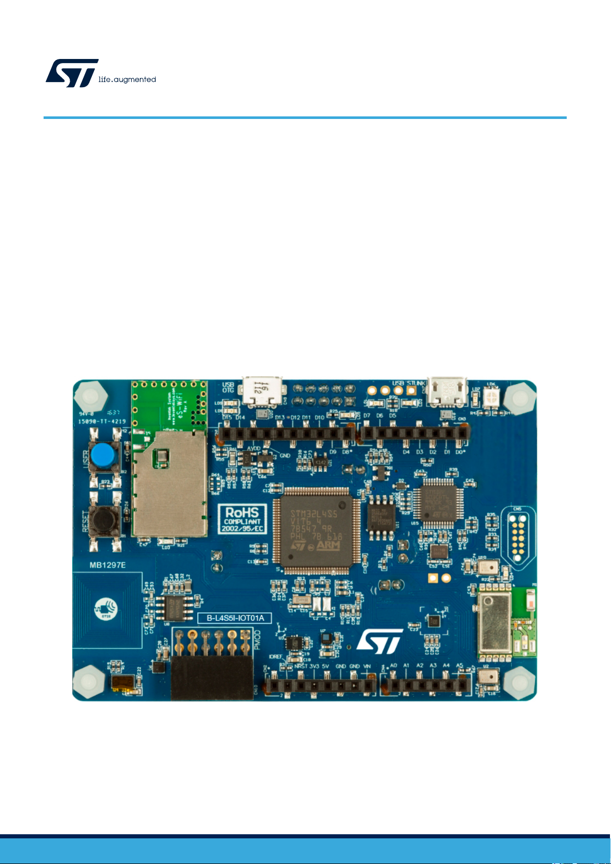
B-L4S5I-IOT01A MB1297 STM32L4S5VIT6U
2.1 Product marking
Evaluation tools marked as “ES” or “E” are not yet qualified and therefore not ready to be used as reference
design or in production. Any consequences deriving from such usage will not be at ST charge. In no event, ST will
be liable for any customer usage of these engineering sample tools as reference designs or in production.
“E” or “ES” marking examples of location:
• On the targeted STM32 that is soldered on the board (For an illustration of STM32 marking, refer to the
STM32 datasheet “Package information” paragraph at the www.st.com website).
• Next to the evaluation tool ordering part number that is stuck or silk-screen printed on the board.
This board features a specific STM32 device version, which allows the operation of any bundled commercial
stack/library available. This STM32 device shows a "U" marking option at the end of the standard part number
and is not available for sales.
In order to use the same commercial stack in his application, a developer may need to purchase a part number
specific to this stack/library. The price of those part numbers includes the stack/library royalties.
2.2 Codification
The meaning of the codification is explained in Table 2.
Table 2. Codification explanation
B-L4S5I-IOT01A Description B-L4S5I-IOT01A
B Discovery kit with a variety of sensors Sensor node
L4S5 MCU product line in STM32 32-bit Arm Cortex MCUs STM32L4R5/S5 in the STM32L4+ Series
ISTM32 Flash memory size:
• I for 2 Mbytes 2 Mbytes
IOT Dedicated to IoT applications Discovery kit for IoT applications
The order code is mentioned on a sticker placed on the top or bottom side of the board.
UM2708
Ordering information
UM2708 - Rev 1 page 3/43

3Development environment
The B-L4S5I-IOT01A Discovery kit for the IoT node runs with the STM32L4S5VI 32-bit microcontroller based on
the Arm® Cortex®-M4 core.
3.1 System requirements
• Windows® OS (7, 8 and 10), Linux® 64-bit, or macOS®
• USB Type-A to Micro-B cable
Note: macOS® is a trademark of Apple Inc. registered in the U.S. and other countries.
All other trademarks are the property of their respective owners.
3.2 Development toolchains
• IAR™ - EWARM (see note)
• Keil® - MDK-ARM (see note)
• STMicroelectronics - STM32CubeIDE
Note: On Windows® only.
3.3 Demonstration software
The demonstration software, included in the STM32Cube MCU Package corresponding to the on-board
microcontroller, is preloaded in the STM32 Flash memory for easy demonstration of the device peripherals in
standalone mode. The latest versions of the demonstration source code and associated documentation can be
downloaded from www.st.com.
UM2708
Development environment
UM2708 - Rev 1 page 4/43

4Conventions
Table 3 provides the conventions used for the ON and OFF settings in the present document.
Table 3. ON/OFF convention
Convention Definition
Jumper JPx ON Jumper fitted
Jumper JPx OFF Jumper not fitted
Jumper JPx [1-2] Jumper fitted between Pin 1 and Pin 2
Solder bridge SBx ON SBx connections closed by 0 Ω resistor
Solder bridge SBx OFF SBx connections left open
Resistor Rx ON Resistor soldered
Resistor Rx OFF Resistor not soldered
UM2708
Conventions
UM2708 - Rev 1 page 5/43

5Delivery recommendations
Before the first use, make sure that no damage occurred to the board during shipment and no socketed
components are not firmly fixed in their sockets or loose in the plastic bag.
UM2708
Delivery recommendations
UM2708 - Rev 1 page 6/43

6Hardware layout and configuration
The B-L4S5I-IOT01A Discovery kit for the IoT node is designed around the STM32L4S5VIT6U target
microcontroller in a 100-pin LQFP package. The hardware block diagram (Refer to Figure 2) illustrates the
connection between the STM32 and peripherals: embedded ST-LINK, ARDUINO® Uno V3 shields, Pmod™
connector, Quad-SPI Flash memory, USB OTG connectors, digital microphones, various ST-MEMS sensors, and
the three RF modules (Wi‑Fi®, Bluetooth®, and NFC). Figure 3 and Figure 4 help users to locate these features
on the B-L4S5I-IOT01A Discovery kit for the IoT node. Figure 5 gives the mechanical dimensions of the B-L4S5I-
IOT01A Discovery kit for the IoT node.
Figure 2. Hardware block diagram
STM32L4S5VIT6
MP34DT01
Digital microphone
RTC
SWD
3.3 V Power
supply
32 KHz Crystal
ST-LINK /
V2-1
GPIOs and
UART3
DFSDM
ISM43362-M3G-L44
Wi-Fi® module
PmodTM (2A) connector
PmodTM (4A) connector
LEDs,
reset and wake-up
buttons
GPIOs
GPIOs and
SPI2
GPIOs and
UART2
HS PHY and
Micro-AB USB
connector
OTG FS
QSPI
64-Mbit Quad-SPI Flash
(MX25R6435F)
VCP UART1
ARDUINO® UNo
Shield connectors
GPIOs,
UART4, and
SPI1
Micro-B
USB
connector
GPIOs and
SPI3
SPBTLE-RF
Bluetooth® module
SPSGRF Sub-GHz
(Spirit) module
not fitted
ST25DV04K NFC
module
GPIOs and
I2C2
LIS3MDL
3-axis magnetometer
LSM6DSL
3D gyroscope
LPS22HB
Digital barometer
HTS221
Humidity and
temperature
VL53L0X
ToF and gesture
detection
STSAFE-A110
Authentication and
security
MP34DT01
Digital microphone
UM2708
Hardware layout and configuration
UM2708 - Rev 1 page 7/43

Figure 3. B-L4S5I-IOT01A Discovery kit for the IoT node layout (top view)
UM2708 - Rev 1 page 8/43
UM2708

Figure 4. B-L4S5I-IOT01A Discovery kit for the IoT node layout (bottom view)
UM2708 - Rev 1 page 9/43
UM2708

Figure 5. B-L4S5I-IOT01A Discovery kit for the IoT node mechanical drawing in millimeters
UM2708 - Rev 1 page 10/43
UM2708

6.1 Embedded STLINK/V2-1
The ST-LINK/V2-1 programming and debugging tool is integrated on the B-L4S5I-IOT01A Discovery kit for the IoT
node. Compared to the ST-LINK/V2 the changes are listed below.
The new features supported on the ST-LINK/V2-1 are:
• USB software re-enumeration
• Virtual COM port interface on USB
• Mass storage interface on USB
• USB power management request for more than 100 mA power on USB
The following features are no more supported on the ST-LINK/V2-1:
• SWIM interface
• Application voltage lower than 3 V
For all general information concerning debugging and programming features common between V2 and V2-1
versions, refer to user manual ST-LINK/V2 in-circuit debugger/programmer for STM8 and STM32 (UM1075) at the
www.st.com website.
6.1.1 Drivers
The ST-LINK/V2-1 requires a dedicated USB driver, which, for Windows 7®, Windows 8® and Windows 10®, is
found at www.st.com.
In case the B-L4S5I-IOT01A Discovery kit for the IoT node is connected to the PC before the driver is installed,
some Discovery board interfaces may be declared as “Unknown” in the PC device manager. In this case, the user
must install the dedicated driver files, and update the driver of the connected device from the device manager as
shown in Figure 6.
Note: Prefer using the “USB Composite Device” handle for a full recovery.
Figure 6. USB composite device
6.1.2 ST-LINK/V2-1 firmware upgrade
The ST-LINK/V2-1 embeds a firmware upgrade mechanism for the in-situ upgrade through the USB port. As the
firmware may evolve during the lifetime of the ST-LINK/V2-1 product (for example new functionalities, bug fixes,
support for new microcontroller families), it is recommended to visit the www.st.com website before starting to use
the B-L4S5I-IOT01A Discovery kit for the IoT node and periodically, to stay up-to-date with the latest firmware
version.
UM2708
Embedded STLINK/V2-1
UM2708 - Rev 1 page 11/43

6.2 Power supply
The B-L4S5I-IOT01A Discovery kit for the IoT node is designed to be powered by a 5 V DC power supply. It is
possible to configure the B-L4S5I-IOT01A Discovery kit for the IoT node to use any of the following five sources
for the power supply: 5V_ST_LINK, 5V_ARD, 5V_USB_FS, 5V_VBAT, and 5V_USB_CHARGER.
In case of external 5 V DC power adapter, the B-L4S5I-IOT01A Discovery kit for the IoT node must be powered
by a power supply unit or by a piece of auxiliary equipment complying with the standard EN-60950-1:
2006+A11/2009, and must be Safety Extra Low Voltage (SELV) with limited power capability.
5V_ST_LINK
(Refer to Figure 7)
This is a 5V DC power with limitation from CN7, the USB type Micro-B connector of ST-LINK/V2-1. In this case,
the JP4 jumper must be fitted between pin 1 and pin 2 to select the 5V_ST_LINK power source on the JP4
silkscreen. This is the default setting. If the USB enumeration succeeds, the 5V_ST_LINK power is enabled, by
asserting the PWR_ENn signal (from STM32F103CBT6). This pin is connected to a power switch ST890, which
powers the board. This power switch features also a current limitation to protect the PC in case of an onboard
short-circuit (Current higher than 750 mA). The B-L4S5I-IOT01A Discovery kit for the IoT node can be powered
from the ST-LINK USB connector CN7, but only the ST-LINK circuit has the power before USB enumeration
because the host PC only provides 100 mA to the board at that time. During the USB enumeration, the B-L4S5I-
IOT01A Discovery kit for the IoT node asks for the 500 mA power to the host PC. If the host is able to provide the
required power, the enumeration finishes by a SetConfiguration command and then, the power transistor ST890 is
switched ON, the red LED LD7 is turned ON, thus the B-L4S5I-IOT01A Discovery kit for the IoT node consumes
up to 500 mA current, but no more. If the host cannot provide the requested current, the enumeration fails.
Therefore the ST890 remains OFF and the MCU part including the extension board is not powered. As a
consequence, the red LED LD7 remains turned OFF. In this case, it is mandatory to use an external power supply.
Figure 7. JP4: 5V_ST_LINK selection
12
3
5
7
4
6
8
109
5V_ST_LINK
5V_ARD
5V_USB_FS
5V_VBAT
5V_USB_CHARGER
JP4
5V_ARD
(Refer to Figure 8)
This is the 7 to 12 V DC power from ARDUINO® CN2 pin 8 (named VIN on ARDUINO® connector silkscreen). In
this case, the JP4 jumper must be fitted between pin 3 and pin 4 to select the 5V_ARD power source on the JP4
silkscreen and the DC power comes from the power supply through the ARDUINO® Uno V3 battery shield
(compatible with Adafruit PowerBoost 500 shield).
UM2708
Power supply
UM2708 - Rev 1 page 12/43

Figure 8. JP4: 5V_ARD selection from CN6 (VIN)
12
3
5
7
4
6
8
109
5V_ST_LINK
5V_ARD
5V_USB_FS
5V_VBAT
5V_USB_CHARGER
JP4
5V_USB_FS
(Refer to Figure 9)
This is the DC power with 500 mA limitation from CN9, the USB OTG FS Micro-AB connector. In this case, the
JP4 jumper must be fitted between pin 5 and pin 6 to select the 5V_USB_FS power source on the JP4 silkscreen.
Figure 9. JP4: 5V_USB_FS
12
3
5
7
4
6
8
109
5V_ST_LINK
5V_ARD
5V_USB_FS
5V_VBAT
5V_USB_CHARGER
JP4
5V_VBAT
(Refer to Figure 10)
This is the DC power coming from an external source. In this case, the JP4 jumper must be fitted between pin 7
and pin 8 to select the 5V_VBAT power source on JP4 silkscreen.
UM2708
Power supply
UM2708 - Rev 1 page 13/43

Figure 10. JP4: 5V_VBAT
12
3
5
7
4
6
8
109
5V_ST_LINK
5V_ARD
5V_USB_FS
5V_VBAT
5V_USB_CHARGER
JP4
5V_USB_CHARGER
(Refer to Figure 11)
This is the DC power charger connected to the USB ST-LINK (CN7). To select the 5V_USB_CHARGER power
source on JP4 silkscreen, the JP4 jumper must be fitted between pin 9 and pin 10. In this case, if the B-L4S5I-
IOT01A Discovery kit for the IoT node is powered by an external USB charger, then the debug is not available. If
the PC is connected instead of the charger, the limitation is no longer effective and the PC may be damaged.
Figure 11. JP4: 5V_USB_CHARGER selection
12
3
5
7
4
6
8
109
5V_ST_LINK
5V_ARD
5V_USB_FS
5V_VBAT
5V_USB_CHARGER
JP4
Note: If the board is powered by a USB charger, there is no USB enumeration, so the LD7 LED remains OFF
permanently and the board is not powered. In this specific case only, the resistor R30 must be soldered, to allow
the board to be powered anyway.
Caution: Do not connect the PC to the ST-LINK (CN7) when R30 is soldered. The PC may be damaged or the board may
not be powered correctly.
UM2708
Power supply
UM2708 - Rev 1 page 14/43

The green LED LD5 is lit when the B-L4S5I-IOT01A Discovery kit for the IoT node is powered by the 5 V correctly.
The power tree is shown in Figure 12. Power tree.
Figure 12. Power tree
USB_ST_LINK
USB_OTG_FS
ARDUINO®
STM32F103 ST_LINK
Bi-color LED
ST_LINK debug
TAG
MCU STM32L4S5VIT6
64-Mbit QSPI Flash
(MX25R6435F)
MP34DT01 digital microphone
ISM43362-M3G-L44
Wi-Fi® module
SPBTLE-RF
Bluetooth® module
SPSGRF Sub-GHz
(Spirit) module
not fitted
ST25DV04K NFC module
LIS3MDL
3-axis magnetometer
LSM6DSL
3D gyroscope
LPS22HB
Digital barometer
HTS221
Humidity and temperature
VL53L0X
ToF and gesture detection
STSAFE-A110
Authentication and security
MP34DT01 digital microphone
LDO
LD1117S33TR
3V3
5V
VDD_MCU
JP5
IC14
JP4
3V3_Wifi
LDO
LT1963EST-3.3
5V
IC12
Pmod™
Power switch 5V/1.2A
ST890CDR
IC17
LDO
LD3985M33R
IC16
5V_ST_Link
5V_ARD
5V_USB_FS
5V_VBAT
5V_USB_charger
LDO
LD1117S50TR
U13
VIN 5V
VDDA
5V_ARD
3V3
5V_ARD
5V_USB_ST_Link
3V3_ST_Link
Switch 5V/1.2A
ST890CDR
IC17
5V
5V_USB_FS
VDDA
UM2708
Power supply
UM2708 - Rev 1 page 15/43

6.3 Programming and debugging when the power supply is not from ST-LINK
(5V_ST_LINK)
It is mandatory to power the board first using CN2 (VIN) or CN9 (USB_FS_OTG), then to connect the USB cable
to the PC. Proceeding this way ensures that the enumeration succeeds, thanks to the external power source. The
following power sequence procedure must be respected:
1. Connect the jumper JP4 on (5V_ARD) or (5V_USB_FS).
2. Connect the external power source to CN2 in case of an ARDUINO® shield or to CN9 in case of USB FS
host interface.
3. Check that the red LED LD5 is turned ON.
4. Connect the PC to the USB connector CN7.
If this sequence is not respected, the board may be powered by VBUS first from ST-LINK, and the following risks
may be encountered:
1. If more than 500 mA current is needed by the board, the PC may be damaged or the current can be limited
by the PC. As a consequence, the board is not powered correctly.
2. 500 mA is requested at the enumeration, so there is a risk that the request is rejected and enumeration does
not succeed if the PC cannot provide such current.
6.4 Clock source
Three clock sources are described below:
• X1 8 MHz oscillator for the STM32L4S5VI microcontroller. This clock is not implemented in a basic
configuration.
• X2 32.768 kHz crystal for the STM32L4S5VI embedded RTC
• X3 8 MHz clock from the ST-LINK MCU for the STM32L4S5VIT6Umicroncontroller.
6.5 Reset sources
The reset signal of the B-L4S5I-IOT01A Discovery kit for the IoT node is active LOW and the reset sources
include:
• A reset button B1
• An ARDUINO® Uno V3 shield board from CN2
• An embedded ST-LINK/V2-1
6.6 USB OTG FS
The B-L4S5I-IOT01A Discovery kit for the IoT node supports USB OTG full-speed communications via the CN9
USB Micro-AB connector.
To do this, the following components must be added by the user:
• 8 MHz crystal (at X1 position). Reference is NX3225GD-8.00M
• 8.2 pF capacitor (0402 size) at the C2 position
• 8.2 pF capacitor (0402 size) at the C4 position
• 0-ohm resistor (0402 size) at the R5 position
• 0-ohm resistor (0402 size) at the R7 position
The B-L4S5I-IOT01A Discovery kit for the IoT node can be powered by the USB connectors at 5 V DC with
500 mA current limitation. A USB power switch (IC19) is also connected to VBUS and provides power to CN9. The
green LED LD9 is lit when either:
• The power switch is ON and the B-L4S5I-IOT01A Discovery kit for the IoT node works as a USB host,
• Or VBUS is powered by another USB host when the B-L4S5I-IOT01A Discovery kit for the IoT node works as
a USB device,
The red LED LD8 is lit when an over-current occurs.
UM2708
Programming and debugging when the power supply is not from ST-LINK (5V_ST_LINK)
UM2708 - Rev 1 page 16/43

6.7 Quad-SPI NOR Flash memory
64-Mbit Quad-SPI NOR Flash memory is connected to the Quad-SPI interface of the STM32L4S5VI
microcontroller.
6.8 Virtual COM port
The serial interface USART1 is directly available as a Virtual COM port of the PC connected to the ST-LINK/V2-1
USB connector CN7. The Virtual COM port settings are configured with 115200 bps, 8-bit data, no parity, one-stop
bit, and no flow control.
6.9 RF modules
Three RF interfaces are available on the B-L4S5I-IOT01A board:
1. Bluetooth® (V4.1 compliant) SPBTLE-RF module,
2. 802.11 b/g/n compliant Wi‑Fi® module ISM43362-M3G-L44 from Inventek Systems,
3. Dynamic NFC Tag based on ST25DV04K with its printed NFC antenna (Double layer inductive antenna
etched on the PCB).
6.9.1 Bluetooth® (V4.1 compliant) SPBTLE-RF module
The ST SPBTLE-RF module (M1) is implemented on the top side of the B-L4S5I-IOT01A Discovery kit for the IoT
node.
The SPBTLE-RF is an easy to use Bluetooth® smart master-slave network processor module, compliant with
Bluetooth® V4.1. The SPBTLE-RF B-Smart module supports multiple roles simultaneously, and it can act at the
same time as Bluetooth® Smart sensor and hub device.
The entire Bluetooth® Smart stack and protocol are embedded into the SPBTLE-RF B-Smart module. The
external host application processor, where the application resides, is connected to the SPBTLE-RF B-Smart
module through a standard SPI interface (SPI3 of STM32L4S5VI).
The SPBTLE-RF B-SmarT module provides a complete RF platform in a tiny form factor (Footprint of this module
is 13.5 mm x 11.5 mm). Radio, antenna, high frequency, and LPO oscillators are integrated to offer a certified
solution to optimize the time to market of the final applications.
Figure 13. SPBTLE-RF module
UM2708
Quad-SPI NOR Flash memory
UM2708 - Rev 1 page 17/43

The main features of the ST SPBTLE-RF module are listed below:
• Bluetooth® V4.1 compliant (Support of master and slave modes, multiple roles supported simultaneously)
• Embedded Bluetooth® low-energy protocol stack (GAP, GATT, SM, L2CAP, LL, RFPHY)
• Bluetooth® Low Energy profiles provided separately
• Bluetooth® radio performance
• Embedded ST BlueNRG-MS
• Tx power: + 4 dBm
• Host interface: SPI, IRQ, and RESET. On-field stack upgrading available via SPI.
• Certification: CE qualified, FCC, IC modular approval certified, BQE qualified
• On-board chip antenna
6.9.2 Inventek Systems ISM43362-M3G-L44 (802.11 b/g/n compliant Wi‑Fi® module)
The Inventek Systems ISM43362-M3G-L44 module (M2) is implemented on the top side of the B-L4S5I-IOT01A
Discovery kit for the IoT node This module is an embedded (eS-WiFi) wireless Internet Connectivity device. The
Wi‑Fi® hardware module consists of an Arm® Cortex®-M3 STM32 host processor, an integrated antenna (or
optional external antenna) and a Broadcom Wi-Fi device. The module uses either a UART or an SPI interface
(UART3 or SPI3 of STM32L4S5VI). By default, an SPI interface is used, as the corresponding firmware (for SPI
capability) is downloaded on the Wi‑Fi® ISM43362-M3G-L44 module. The Wi‑Fi® module requires no operating
system and has a completely integrated TCP/IP stack that only requires AT commands to establish connectivity
for a wireless product. The footprint of this module is 14.5 mm x 30 mm.
Figure 14. ISM43362-M3G-L44 module
UM2708
RF modules
UM2708 - Rev 1 page 18/43

The main features of the Inventek system ISM43362-M3G-L44 module are:
• Based on the Broadcom BCM43362 MAC/Baseband/Radio device
• Supports Broadcom WICED SDK
• CPU Arm® Cortex®-M3 32-bit RISC core from STMicroelectronics
• IEEE 802.11n D7.0, OFDM-72.2 Mbps, single-stream width of 20 MHz, and short GI
• IEEE 802.11g, OFDM 54 Mbps
• IEEE 802.11b, DSSS 11 Mbps
• IEEE 802.11i, Security
– WPA (Wi‑Fi® Protected Access) –PSK/TKIP
– WPA2 (Wi‑Fi® Protected Access 2) –AES/CCMP/802.1x authentication
• GPIO, 5 ADC (SPI interface utilizes ADC pins)
• Power-saving mode allows the design of low-power applications
• Lead-free design which is compliant with ROHS requirements
• EMI/EMC Metal Shield for best RF performance in noisy environments and to accommodate for lower RF
emissions/signature for easier FCC compliance
• FCC/CE compliance certification
On MB1297 revision E, the firmware revision inside the Wi‑Fi® module must be C3.5.2.5.STM. The Wi‑Fi®
module maximum output power is limited to 9 dBm to fulfill FCC/IC/CE requirements. A Wi‑Fi® output power
higher than 9 dBm at the Wi‑Fi® antenna is prohibited.
Note: Since Wi
‑
Fi® and Bluetooth® Low Energy modules are using the same frequency ISM band (2.4 GHz to
2.485 GHz), the simultaneous activity of both modules may affect the RF performances of Wi
‑
Fi® or Bluetooth®
Low Energy (in terms of range or throughput).
6.9.3 Dynamic NFC Tag based on ST25DV04K with its printed NFC antenna
The ST25DV04K device is an NFC RFID Tag offering 4 Kbit of electrically erasable programmable memory
(EEPROM). ST25DV04K offers two interfaces. The first one is an I2C serial link and can be operated from a DC
power supply. The second one is an RF-link activated when ST25DV04K acts as a contactless memory powered
by the received carrier electromagnetic wave.
In I2C mode, the ST25DV04K user memory contains up to 512 bytes which could be split into four flexible and
protectable areas. In RF mode, following ISO/IEC 15693 or NFC forum type 5 recommendations, ST25DV04K
user memory contains up to 128 blocks of 4 bytes which can be split into four flexible and protectable areas.
ST25DV04K offers a fast transfer mode between the RF and contact worlds, thanks to a 256-byte volatile buffer
(also called Mailbox). In addition, the GPO pin of the ST25DV04K provide data informing the contact world about
incoming events, like RF field detection, RF activity in progress or mailbox message availability. An energy
harvesting feature is also proposed when external conditions make it possible.
The main features of the ST25DV04K are:
I2C interface
•Two-wire I2C serial interface supporting 1MHz protocol
• Single supply voltage from 1.8 V to 5.5 V
• Multiple bytes write programming, up to 256 bytes
Contactless interface
• Based on ISO/IEC 15693
• NFC Forum Type 5 tag certified by the NFC Forum
• Support of all ISO/IEC 15693 modulations, coding, sub-carrier modes, and data rates
• Custom fast read access up to 53 Kbps
• Single and multiple blocks read (same for extended commands)
• Single and multiple blocks write (up to 4) (same for extended commands)
• Internal tuning capacitance: 28.5 pF
UM2708
RF modules
UM2708 - Rev 1 page 19/43

Memory
• Up to 64 kbits of EEPROM (depending on the version)
• I2C interface access bytes
• RF interface access blocks of 4 bytes
• Write time:
– From I2C: typical 5 ms for 1 byte
– From RF: typical 5 ms for 1 block
• Data retention: 40 years
• Write cycles endurance:
– 1 million write cycles at 25 °C
– 600k write cycles at 85 °C
– 500k write cycles at 105 °C
– 400k write cycles at 125 °C
Fast transfer mode
•Fast data transfer between I2C and RF interfaces
• Half-duplex 256-byte dedicated buffer
Energy harvesting
• Analog output pin to power external components
Data protection
• User memory: One to four configurable areas, protectable in reading and/or write by three 64-bit passwords
in RF and one 64-bit password in I2C
• System configuration: protected in write by a 64-bit password in RF and a 64-bit password in I2C
Note: The hardware layout is ready to support a Sub-GHz low-power-programmable RF module (SPSGRF-868 or
SPSGRF-915). The footprint is implemented (M3 designation), but no module is soldered.
6.10 STMicroelectronics sensors
Several STMicroelectronics sensors are available on the B-L4S5I-IOT01A Discovery kit for the IoT node and are
listed below:
• Two on-board ST-MEMS audio sensor omnidirectional digital microphones (MP34DT01)
• Capacitive digital sensor for relative humidity and temperature (HTS221)
• High-performance 3-axis magnetometer (LIS3MDL)
• 3D accelerometer and 3D gyroscope (LSM6DSL)
• 260 hPa to 1260 hPa absolute digital output barometer (LPS22HB)
• Time-of-Flight and gesture detection sensor (VL53L0X)
6.10.1 Two on-board ST-MEMS microphones (MP34DT01)
The MP34DT01 is an ultra-compact, low-power, omnidirectional, digital ST-MEMS microphone built with a
capacitive sensing element and an IC interface.
The sensing element, capable of detecting acoustic waves, is manufactured using a specialized silicon
micromachining process dedicated to producing audio sensors.
The IC interface is manufactured using a CMOS process that allows designing a dedicated circuit able to provide
a digital signal externally in PDM format.
The MP34DT01 has an acoustic overload point of 120 dBSPL with a 63 dB signal-to-noise ratio and –26 dBFS
sensitivity.
UM2708
STMicroelectronics sensors
UM2708 - Rev 1 page 20/43
Table of contents
Other ST Motherboard manuals

ST
ST EVALST-ISOSD61L User manual

ST
ST STM32746G-EVAL User manual

ST
ST X-NUCLEO-IDW01M1 User manual

ST
ST STEVAL-IHM031V1 User manual

ST
ST STEVAL-ICB008V1 User manual

ST
ST STM3210B-EVAL User manual

ST
ST EVAL-L9958 User manual

ST
ST VIPower VIPer22A-E Installation and operating instructions

ST
ST STM32439I-EVAL User manual

ST
ST STM32L4R9I-EVAL User manual