ST STM8L101-EVAL User manual

November 2009 Doc ID 15312 Rev 2 1/26
UM0629
User Manual
STM8L101-EVAL
evaluation board
Introduction
The STM8L101-EVAL is composed of two boards:
■An STM8L1/L2 motherboard called MB709 which includes all peripherals which are
connected to the MCU on the daughterboard. The motherboard connects to the
daughterboard via two 36-pin connectors.
■An STM8L1 daughterboard called MB710 which has an STM8L101 MCU.
The motherboard and daughterboard are a complete development platform for
STMicroelectronic's STM8L101 microcontroller with comparator, I2C, SPI, USART and
SWIM debugging support.
The full range of hardware features on the STM8L101-EVAL helps you to evaluate all
peripherals (MicroSD cardTM, USART, EEPROM, LCD, for example) and develop your own
applications.
Figure 1. STM8L101-EVAL board
www.st.com
Downloaded from Elcodis.com electronic components distributor

Contents UM0629
2/26 Doc ID 15312 Rev 2
Contents
1 Overview . . . . . . . . . . . . . . . . . . . . . . . . . . . . . . . . . . . . . . . . . . . . . . . . . . 4
1.1 Features . . . . . . . . . . . . . . . . . . . . . . . . . . . . . . . . . . . . . . . . . . . . . . . . . . . 4
1.2 Demonstration software . . . . . . . . . . . . . . . . . . . . . . . . . . . . . . . . . . . . . . . 4
1.3 Order code . . . . . . . . . . . . . . . . . . . . . . . . . . . . . . . . . . . . . . . . . . . . . . . . . 4
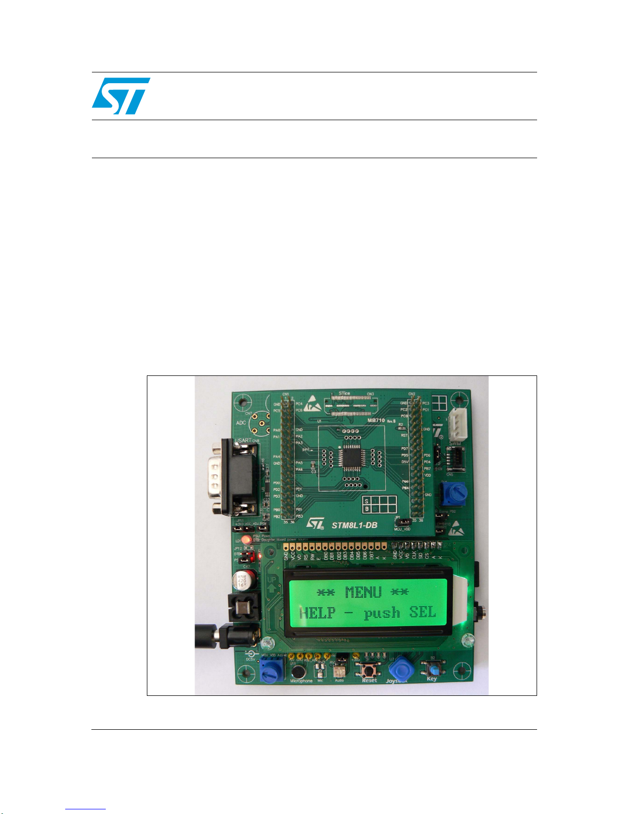
1.4 Hardware layout and configuration . . . . . . . . . . . . . . . . . . . . . . . . . . . . . . . 5
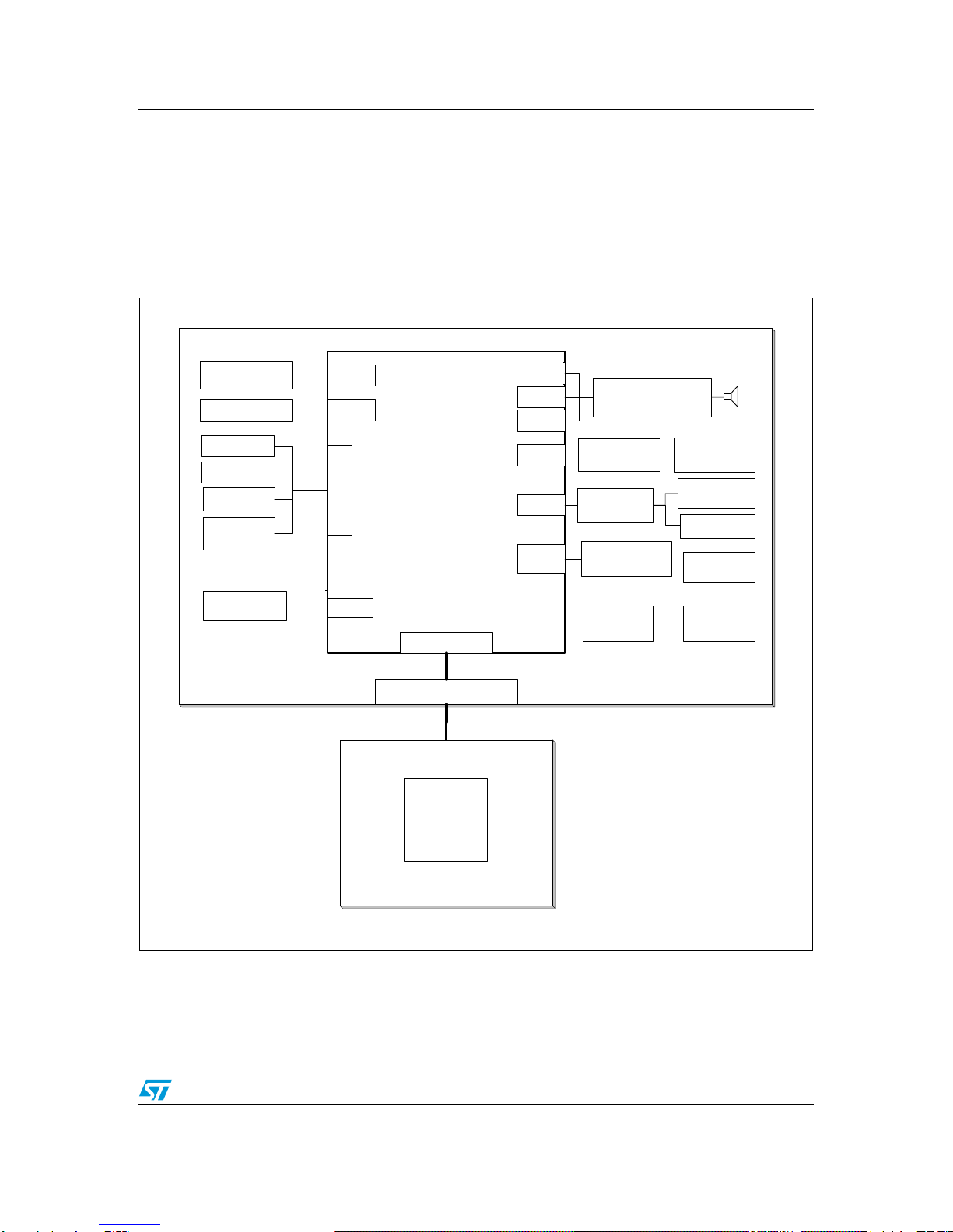
2 STM8L1/L2 motherboard . . . . . . . . . . . . . . . . . . . . . . . . . . . . . . . . . . . . . 8
2.1 Power supply . . . . . . . . . . . . . . . . . . . . . . . . . . . . . . . . . . . . . . . . . . . . . . . 8
2.2 Reset source . . . . . . . . . . . . . . . . . . . . . . . . . . . . . . . . . . . . . . . . . . . . . . . 9
2.3 Audio . . . . . . . . . . . . . . . . . . . . . . . . . . . . . . . . . . . . . . . . . . . . . . . . . . . . . 9
2.4 I2C EEPROM . . . . . . . . . . . . . . . . . . . . . . . . . . . . . . . . . . . . . . . . . . . . . . 10
2.5 RS-232 . . . . . . . . . . . . . . . . . . . . . . . . . . . . . . . . . . . . . . . . . . . . . . . . . . . 10
2.6 MicroSD card . . . . . . . . . . . . . . . . . . . . . . . . . . . . . . . . . . . . . . . . . . . . . . 10
2.7 Analog input . . . . . . . . . . . . . . . . . . . . . . . . . . . . . . . . . . . . . . . . . . . . . . . 10
2.8 Development and debug support CN5 and CN6 . . . . . . . . . . . . . . . . . . . 10
2.9 Display and input devices . . . . . . . . . . . . . . . . . . . . . . . . . . . . . . . . . . . . . 11
2.10 Bi-color LED . . . . . . . . . . . . . . . . . . . . . . . . . . . . . . . . . . . . . . . . . . . . . . . 11
2.11 Economic measurement and potentiometer RV1 . . . . . . . . . . . . . . . . . . . 11
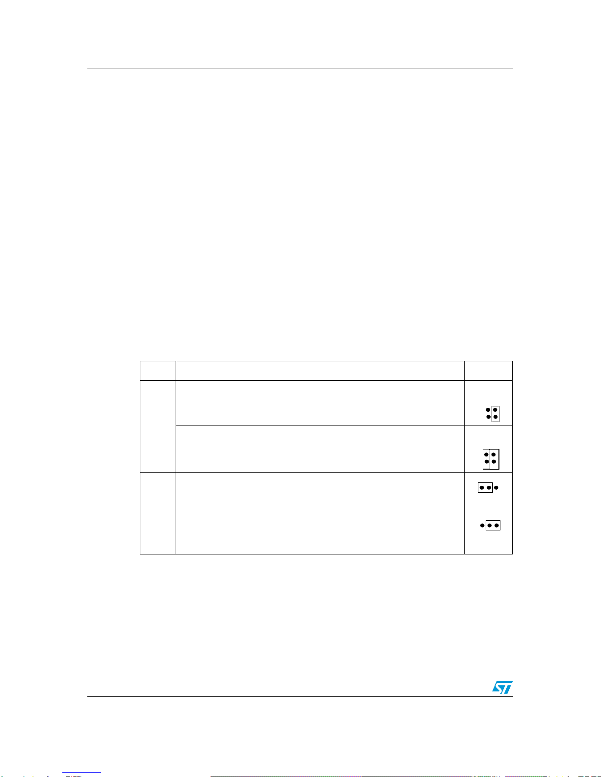
2.12 MicroSD connector CN1 . . . . . . . . . . . . . . . . . . . . . . . . . . . . . . . . . . . . . . 12
2.13 Daughterboard extension connectors CN3 and CN4 . . . . . . . . . . . . . . . . 13
2.14 SWIM connectors CN5 and CN6 . . . . . . . . . . . . . . . . . . . . . . . . . . . . . . . 14
2.15 RS-232 connector CN8 . . . . . . . . . . . . . . . . . . . . . . . . . . . . . . . . . . . . . . 15
2.16 Audio jack CN9 . . . . . . . . . . . . . . . . . . . . . . . . . . . . . . . . . . . . . . . . . . . . . 15
2.17 Power connector CN10 . . . . . . . . . . . . . . . . . . . . . . . . . . . . . . . . . . . . . . 15
3 STM8L1 daughterboard . . . . . . . . . . . . . . . . . . . . . . . . . . . . . . . . . . . . . 16
3.1 Power . . . . . . . . . . . . . . . . . . . . . . . . . . . . . . . . . . . . . . . . . . . . . . . . . . . . 16
3.2 Extension connector CN1 and CN2 . . . . . . . . . . . . . . . . . . . . . . . . . . . . . 16
4 Schematics . . . . . . . . . . . . . . . . . . . . . . . . . . . . . . . . . . . . . . . . . . . . . . . 17
4.1 STM8L1/L2 motherboard . . . . . . . . . . . . . . . . . . . . . . . . . . . . . . . . . . . . . 17
4.2 STM8L1-DB daughterboard schematic . . . . . . . . . . . . . . . . . . . . . . . . . . 23
Downloaded from Elcodis.com electronic components distributor

UM0629 Contents
Doc ID 15312 Rev 2 3/26
Appendix A STM8L101-EVAL I/O assignment . . . . . . . . . . . . . . . . . . . . . . . . . . . 24
5 Revision history . . . . . . . . . . . . . . . . . . . . . . . . . . . . . . . . . . . . . . . . . . . 25
Downloaded from Elcodis.com electronic components distributor

Overview UM0629
4/26 Doc ID 15312 Rev 2
1 Overview
1.1 Features
■5 V power jack supply
■Audio play
■MicroSD cardTM
■64 Kbit I2C EEPROM
■One channel of RS-232 communication
■Bi-color LED
■Economic analog voltage measurement based on comparator
■SWIM debug support
■122 x 32 dot-matrix serial interface LCD module
■Joystick with 4-direction control and selector
■Reset and User button
■3 LEDs
■Extension connector for daughterboard
■One 10 K potentiometer
■RoHS compliant
1.2 Demonstration software
Demonstrationsoftware is preloaded in the board’s Flash memory for easy demonstration of
device peripherals in stand-alone mode. For more information and to download the latest
version available, refer to STM8L101-EVAL demonstration firmware available on web:
www.st.com/mcu.
1.3 Order code
To order the STM8L101K3 evaluation board, use the order code STM8L101-EVAL.
Downloaded from Elcodis.com electronic components distributor

UM0629 Overview
Doc ID 15312 Rev 2 5/26
1.4 Hardware layout and configuration
The STM8L101-EVAL evaluation board is designed around the STM8L101K3T6 in an
LQFP32 package.
Figure 2 illustrates the connections between the daughterboard and the peripherals on the
motherboard (LCD, I2C EEPROM, USART, audio and MicroSD card).
Figure 3 and Figure 4 help you to locate these features on the actual evaluation board.
Figure 2. Hardware block diagram
STM8L1/L2-MB
RS232
transceiver
5V power
jack
3.3V
regulator
LCD
MicroSD card
Level
translator
Audio circuit
BNC connector
I2C EEPROM
SWIM connector
STice connector
Push button
Joystick
LED’s
Potentiometer
RS232
connector
SWIM
GPIO’s
ADC
ADC
PWM
USART
Compa
rator
SPI
I2C
Economic
Measurement
BEEP
1.8 to 3.3V
regulator
Bi-color LED
GPIO’s
Extension connector
STM8L1-DB
STM8L1/L2-MB (MB709)
STM8L101
MCU
STM8L1-DB (MB710)
CMP
Downloaded from Elcodis.com electronic components distributor

Overview UM0629
6/26 Doc ID 15312 Rev 2
Figure 3. STM8L1/L2 motherboard layout
RV4
MCU_VDD
CN9
Audio jack
CN1
Micro
RV1
Potentiometer
B1
RESET U7
Joystick B2
KEY
U2
Dot-matrix LC
D
CN5
SWIM
adjustment
CN8
USART
CN10
5V power
CN3, CN4 daughterboard connectors
SD card™
CN6
SWIM
alternative)
(ERNI cable
Downloaded from Elcodis.com electronic components distributor

UM0629 Overview
Doc ID 15312 Rev 2 7/26
Figure 4. STM8L1 daughterboard layout
CN1, CN2 motherboard connector
STM8L101 MCU in LQFP32 package
soldered directly onto the board
and footprint for socket (ref ENPLAS OTQ-32-0.8-02) is present on the board
Downloaded from Elcodis.com electronic components distributor

STM8L1/L2 motherboard UM0629
8/26 Doc ID 15312 Rev 2
2 STM8L1/L2 motherboard
This motherboard is designed to work with an STM8L1 daughterboard.
2.1 Power supply
The motherboard is designed to be powered by a 5 V DC power supply and to be protected
from a wrong power plug-in event by PolyZen Inc. (auto rearmable fuse) U13. It is possible
to configure the evaluation board to provide 5 V power to the daughterboard through the
daughterboard connector.
●The motherboard is powered by a 5 V DC power adapter connected to CN10, the
power jack on the board (PSU on silk screen for power supply unit).
●5 V DC power is provided to the daughterboard through an extension connector and
can be set by jumper JP12 (DTB for daughterboard on silk-screen).
●MCU_VDD can be selected by setting jumper JP11 and is connected to the
daughterboard directly through the daughterboard connector.
The power supply is configured by setting the jumpers JP11 and JP12 as described in
Table 1.
The LED LD6 is lit when the motherboard is powered correctly. JP3 is no longer used.
Table 1. Power related jumpers
Jumper Description Setting
JP12
5 V power from power supply jack (CN10) is connected to the motherboard
when JP12 is set as shown to the right:
(default setting).
5 V power from power supply jack (CN10) is connected to the daughterboard
when JP12 is set as shown to the right:
In this case the motherboard and daughterboard are powered by a 5 V power
supply.
JP11
MCU_VDD is powered by a fixed 3.3 V power supply when JP11 is set as
shown to the right:
(default setting).
MCU_VDD is powered by a variable power supply from 1.8 V to 3.3 V,
adjusted by potentiometer RV4 (bottom left of the board), when JP11 is set as
shown to the right:
PSU
DTB PSU
DTB
1
1
Downloaded from Elcodis.com electronic components distributor

UM0629 STM8L1/L2 motherboard
Doc ID 15312 Rev 2 9/26
2.2 Reset source
The reset signal of the motherboard is low active. Reset sources include:
●Reset button B1.
●Debugging tools from connectors CN5, CN6.
The reset pin PA1 of the STM8L101 is either connected to the reset button B1 or to GND by
the setting of jumper JP1:
2.3 Audio
The motherboard supports both audio recording and playback, but audio recording
components (U11 microphone and U12 amplifier) cannot be used with the STM8L101.
The speaker can be disabled or enabled by the setting of jumper JP10.
Audio volume can be adjusted using the potentiometer RV2.
Table 2. Reset related jumpers
Jumper Description Setting
JP1
PA1 is connected to GND when JP1 is set as shown to the right:
This configuration is reserved for internal use only.
PA1 is connected to Reset button when JP1 is set as shown to the right:
(default setting).
This jumper position is called Alone on the silk-screen.
1 2 3
1 2 3
Table 3. Audio related jumpers
Jumper Description Setting
JP10 Audio power amplifier TS4871 is forced on standby mode when JP10 is
not fitted.
Default setting: fitted.
JP9
Either beeper or PWM output can be selected as a source of speaker
by setting jumper JP9.
The beeper is connected to speaker when JP9 is set as shown to the
right: (Beep position on the silk-screen).
The PWM output is connected to speaker when JP9 is set as shown to
the right: (PSW position on the silk-screen) (default setting).
1 2 3
1 2 3
Downloaded from Elcodis.com electronic components distributor

STM8L1/L2 motherboard UM0629
10/26 Doc ID 15312 Rev 2
2.4 I2C EEPROM
A 64 Kbit I2C EEPROM is connected to the I2C port of the STM8L101.
Write protection can be enabled by the setting of jumper JP8.
2.5 RS-232
One D-type 9-pin RS-232 connector CN8 is available on the motherboard.
RS-232 interface behavior is not guaranteed when the MCU is powered by an adjustable
voltage lower than 3 V.
Note: To communicate with an RS-232 port on a PC, a 9-pin straight RS-232 cable (direct pin to
pin connection) is needed because:
●
On CN8 the RX signal is connected on pin2 and the TX data on pin 3,
●
On the PC side the RX signal is generally on pin 3 and the TX signal on pin 2.
This standard 9-pin straight RS-232 cable is not provided with the board. Refer to
Section 2.15 for details on RS-232 connector pinout.
2.6 MicroSD card
The 1GByte (or more) MicroSD card connected to the SPI of the STM8L101 through a
voltage level translator U1 (shared with LCD) is available on the board. MicroSD card chip
select is managed by standard I/O port PB4.
2.7 Analog input
The BNC connector footprint present on the board (CN7) cannot be used as it is not
connected to the MCU.
2.8 Development and debug support CN5 and CN6
The two debug connectors are available on the motherboard.
●CN5, ERNI 4-pin connector (reference 284697 or 214017) for SWIM debugging. It fits
with ERNI connectors provided with standard tools.
●CN6, 2.54 mm pitch low-cost 4-pin connector for SWIM debugging.
Table 4. I2C EEPROM related jumpers
Jumper Description
JP8 I2C EEPROM U6 is protected from write operation when JP8 is not fitted.
Default setting: Fitted
Downloaded from Elcodis.com electronic components distributor

UM0629 STM8L1/L2 motherboard
Doc ID 15312 Rev 2 11/26
2.9 Display and input devices
Display devices available are:
●122x32 dot-matrix serial interface LCD (U2)
●4 general purpose LED's (LD2,3,4,5)
Input devices available are:
●4-direction joystick
●selection key
●general purpose button (B2)
2.10 Bi-color LED
A bi-color LED is connected to PB0 through a voltage translator which guarantees that the
bi-color LED works when the STM8L101 is powered by an adjustable voltage from 1.8 V to
3.3 V.
2.11 Economic measurement and potentiometer RV1
The economic measurement solution is demonstrated based on the internal comparator
inside the STM8L101 and potentiometer RV1.
As shown in Figure 5, the voltage divided by resister bridge R10 and R11 can be measured
by using an internal comparator of the STM8L1, with Vref connected to channel 2 of the
comparator and an RC charge circuit connected to the COM channel of the comparator.
To measure the voltage Vin from the potentiometer:
1. Compare Vref with the voltage on C8 which is charged by a series of pulses generated
by PC4.
2. Record pulse number PN_Vref when the voltage on C8 reaches voltage reference Vref.
3. Another charge pulse PN_Vin can be obtained with voltage connected to CH1 also like
PN_Vref.
4. The voltage Vin can be calculated based on both numbers PN_Vref and PN_Vin.
Table 5. 122x32 dot matrix LCD U13
Pin on U2 Description Pin connection
1 Vss GND
2Vcc+3V3
3VO-
4 CLK PB5
5 SID PB6
6CSPD1
7A+5V
8KGND
Downloaded from Elcodis.com electronic components distributor

STM8L1/L2 motherboard UM0629
12/26 Doc ID 15312 Rev 2
Figure 5. Voltage measurement using internal comparator
2.12 MicroSD connector CN1
Figure 6. MicroSD connector CN1 viewed from front
Table 6. Potentiometer RV1 related jumpers
Jumper Description Setting
JP2
RV1 is connected to PD2 as one input of the internal comparator when JP2
is set as shown to the right:
JP2 position is called Comp_PD2 on the silk-screen.
RV1 is not connected when JP2 is set as shown to the right:
(default setting). JP2 position is called ADC_PE0 on the silk-screen.
1 2 3
1 2 3
Downloaded from Elcodis.com electronic components distributor

UM0629 STM8L1/L2 motherboard
Doc ID 15312 Rev 2 13/26
2.13 Daughterboard extension connectors CN3 and CN4
Two 36-pin male headers CN3 and CN4 can be used to connect the daughterboard to the
motherboard. All GPI/Os are available on it. Please refer to Table 8 and Table 9 for pin-out
definition.
Table 7. MicroSD connector CN1
Pin number Description Pin number Description
1 Reserved 5 SCLK/PB5
2 CS/PB4 6 Vss/GND
3 DI/PB6 7 DO/PB7
4VDD8Reserved
9 GND 10 Not used
Table 8. Daughterboard extension connector CN3
Pin number Description Pin number Description
1 GND 2 PC4
3PC54PC6
5 Reserved 6 Reserved
7 Reserved 8 Reserved
9PA010GND
11 PA1 12 PA2
13 Reserved 14 PA3
15 Reserved 16 Reserved
17 PA4 18 Reserved
19 GND 20 PA5
21 Reserved 22 PA6
23 Reserved 24 Reserved
25 PD0 26 Reserved
27 PD2 28 PD1
29 PD3 30 GND
31 NC 32 NC
33 PB0 34 PB1
35 PB2 36 PB3
Downloaded from Elcodis.com electronic components distributor

STM8L1/L2 motherboard UM0629
14/26 Doc ID 15312 Rev 2
2.14 SWIM connectors CN5 and CN6
CN6 is a low cost 2.54 mm pitch connector to be used by customers who do not have the
ERNI cable.
Figure 7. SWIM debugging connector CN5 viewed from above PCB
Table 9. Daughterboard extension connector CN4
Pin number Description Pin number Description
1 GND 2 PC3
3PC24PC1
5PC06Reserved
7 Reserved 8 Reserved
9 Reserved 10 GND
11 RESET# 12 Reserved
13 Reserved 14 Reserved
15 PD7 16 Reserved
17 PD5 18 PD6
19 D5V 20 PD4
21 NC 22 PB7
23 NC 24 MCU_VDD
25 PB6 26 PB5
27 PB4 28 Reserved
29 Reserved 30 GND
31 Reserved 32 Reserved
33 Reserved 34 Reserved
35 Reserved 36 Reserved
Table 10. SWIM debugging connectors CN5 and CN6
Pin number Description Pin number Description
1VDD2PA0
3 GND 4 RESET#
Downloaded from Elcodis.com electronic components distributor

UM0629 STM8L1/L2 motherboard
Doc ID 15312 Rev 2 15/26
2.15 RS-232 connector CN8
Figure 8. RS-232 connector CN8 viewed from front
2.16 Audio jack CN9
A 3.5 mm mono audio jack CN9 is available on the motherboard. The speaker U9 is
bypassed when an earphone is plugged into CN9 (CN9 is compatible with audio plug
NYS231 from NEUTRIK).
2.17 Power connector CN10
The motherboard can be powered from a DC 5 V power supply via the external power
supply jack CN10 shown in Figure 9. The central pin of CN10 must be positive.
Figure 9. Power supply connector CN10 viewed from front
Table 11. RS-232 connector CN8
Pin number Description Pin number Description
1 NC 6 Connect to Pin 4
2 USART_RXD/PC2 7 Connect to Pin 8
3 USART_TXD/PC3 8 Connect to Pin 7
4 Connect to Pin 6 9 NC
5GND
Downloaded from Elcodis.com electronic components distributor

STM8L1 daughterboard UM0629
16/26 Doc ID 15312 Rev 2
3 STM8L1 daughterboard
3.1 Power
The STM8L101 MCU is powered by MCU_VDD from the motherboard through an extension
connector on the board. It is enabled by setting the jumper JP1 as described in Table 12.
3.2 Extension connector CN1 and CN2
The 36-pin connectors CN1 and CN2 are designed to be connected to the motherboard.
The pin-out definition is the same as CN3 and CN4 on the motherboard which is described
in Section 2.13.
Warning: On MB710 PCB rev B, CN2 (pin 26) silk-screen PB5 is missing
Table 12. Power related jumper*
Jumper Description
JP1 Enables consumption measurement of VDD when the jumper is removed and replaced by
an ammeter.
Default setting: Fitted.
Downloaded from Elcodis.com electronic components distributor

UM0629 Schematics
Doc ID 15312 Rev 2 17/26
4 Schematics
4.1 STM8L1/L2 motherboard
Figure 10. STM8L1 motherboard schematic
STMicroelectronics
Title:
Number: Rev: Sheet of
A.1(PCB.SCH)
Date:
1/21/2009MB709 1 6
STM8L1/L2-MB
Audio_PWM
MIC_OUT
BEEP
U_Audio
Audio.SchDoc
MicroSD_CS
SPI_SCK
SPI_MOSI
LCD_CS
SPI_MISO
SDcard_detect
U_LCD_MicroSD
LCD_MicroSD.SchDoc
MicroSD_CS
SPI_SCK
SPI_MOSI
LCD_CS
SPI_MISO
Audio_PWM
MIC_OUT
BEEP
BNC
Potentiometer
I2C_SLK
I2C_SDA
LED4
LED3
LED1
LED2
JOY_SEL
JOY_DOWN
JOY_LEFT
JOY_RIGHT
JOY_UP
User_Button
USART_TX
USART_RX
BiD_LED
SDcard_detect
U_MCU
MCU.SchDoc
BNC
Potentiometer
I2C_SLK
I2C_SDA
LED4
LED3
LED1
LED2
JOY_SEL
JOY_DOWN
JOY_LEFT
JOY_RIGHT
JOY_UP
User_Button
BiD_LED
USART_RX
USART_TX
U_Peripherals
Peripherals.SchDoc
U_Power
Power.SchDoc
Downloaded from Elcodis.com electronic components distributor

Schematics UM0629
18/26 Doc ID 15312 Rev 2
Figure 11. STM8L1 motherboard MCU
STMicroelectronics
Title:
Number: Rev: Sheet of
A.1(PCB.SCH)
Dat e:
10/12/2009MB709 2 6
STM8L1/L2-MB MCU
MicroSD_CS
SPI_SCK
SPI_MOSI
LCD_CS
SPI_MISO
Audi o_PWM
MIC_OUT
BEEP
BNC
Potentiometer
I2C_SL K
I2C_SD A
LED4
LED3
LED1
LED2
JOY_SEL
JOY_DOWN
JOY_LEFT
JOY_RIGHT
JOY_UP
User_Button USA RT_TX
USA RT_RX
1
4 3
2
B1
RESET
R15
10K
MCU_VDD
C5
100nF
RESET#
32
1JP1
C9
20pF C10
20pF
X1
Not Fi tted
R17 60
BiD_LED
L1
BEAD C11
10uF C12
10nF
JP3
Not F itted C7
100nF
VDD
VDD VDDA
C6
100nF
MCU_VDD
PA1
PA2
PA4
PA5
PA6
PG0
PG1
PG2
PG3
PD0
PD1
PD2
PD3
PB0
PB1
PB2
PB3
PE0
PE1
PE2
PE3
PE4
PE5 PE6
PE7
PB4
PB5
PB6
PB7
PD4
PD5
PD6
PD7
PF0
PF1
PF2
PF3
PF4
PF5
PF6
PF7
PC0
PC1
PC2
PC3
PC4
PC5
PC6
PC7
PH0
PH1
PH2
PA0
VDD
VDDA
PG4
PG5
PG6
PG7
VDD
PA3
PA1/NRST
1
PA2/HSE_IN
2
PA3/HSE_OUT
3
PA4/ADC_IN15/TIM2_BKIN
8
PG4
4
PG5
5
PG6
6
PG7
7
PA5/ADC_IN14/TIM3_BKIN
9
PA6/ADC_IN13/COMP_REF
10
VSSA
11
VSS
12
VDD
13
VDDA
14
PG0/REF+
15
PG1/REF-
16
PG2/ADC_IN12
17
PG3/ADC_IN11
18
PD0/TIM3_CH2/COMP1_CH3
19
PD1/TIM3_TRIG/COMP1_CH4
20
PD2/COMP2_CH3
21
PD3/COMP2_CH4
22
PB0/TIM2_CH1/COMP1_CH1
23
PB1/TIM3_CH1/COMP1_CH2
24
PB2/ TIM2_CH2/COMP2_CH1
25
PB3/TIM2_TRIG/COMP2_CH2
26
PE0/ADC_IN2
27
PE1/ADC_IN1
28
PE2/ADC_IN0
29
PE3
30
PE4
31
PE5
32 PE6 33
PE7 34
PB4/SPI_NSS 35
PB5/SPI_SCK 36
PB6/SPI_MOSI 37
PB7/SPI_MISO 38
VSS 39
VDD 40
PD4 41
PD5 42
PD6 43
PD7 44
PF0 45
PF1 46
PF2 47
PF3 48
PF4 49
PF5 50
PF6 51
PF7 52
PC0/I2C_SDA 53
PC1/I2C_SCL 54
PC2/USART_RX 55
PC3/USART_TX 56
PC4/USART_CK/CCO 57
PC5/LSE_IN 58
PC6/LSE_OUT 59
PC7 60
PH0 61
PH1 62
PH2 63
PA0/SWIM/BEEP/IR_TIM 64
U4
Not F itted
MCU_VDD
1
2
3
4
CN6
609-1306-ND(2.54mm)
1
2
3
4
CN5
214017
RESET# R9 0
PA0
SWIM connector
SWIM connector
SWIM connector
1
23
JP2
1 2
3 4
5 6
7 8
910
11 12
13 14
15 16
17 18
19 20
21 22
23 24
25 26
27 28
29 30
31 32
33 34
35 36
37 38
39 40
41 42
43 44
45 46
47 48
49 50
51 52
53 54
55 56
57 58
59 60
61 62
63 64
65 66
67 68
69 70
71 72
73 74
75 76
77 78
79 80
81 82
83 84
85 86
87 88
89 90
91 92
93 94
95 96
97 98
99 100
101 102
103 104
105 106
107 108
109 110
111 112
113 114
115 116
117 118
119 120
G1 G4
G1 G4
G2 G3
G2 G3
CN2
Not F itted
RESET# PA2
PA4
PA5 PA6
PG0 PG1
PG2 PG3
PD0 PD1
PD2 PD3
PB0 PB1
PB2 PB3
PE0 PE1
PE2 PE3
PE4 PE5
VDD VDDA
PG4
PG5 PG6
PG7
PA3
PE6 PE7
PB4 PB5
PB6 PB7
PD4 PD5
PD6 PD7
PF0 PF1
PF2 PF3
PF4 PF5
PF6 PF7
PC0 PC1
PC2 PC3
PC4
PC7PH0 PH1PH2 PA0
VDD
R18 820
1 2
3 4
5 6
7 8
910
11 12
13 14
15 16
17 18
19 20
21 22
23 24
25 26
27 28
29 30
31 32
33 34
35 36
CN3
Header 18X2 on the left
1 2
3 4
5 6
7 8
910
11 12
13 14
15 16
17 18
19 20
21 22
23 24
25 26
27 28
29 30
31 32
33 34
35 36
CN4
Header18X2 on theright
D5V
RESET#
Exension connector
MCU_VDD
C8
100nF
R14
10K PA6PC4
R11
8K
R10
25K
PE0
PD2
+3V3
R12
29K
R13
4K
PD3
Comparator
STice connector
MCU
Economic measurement
PA1 PA2
PA4 PA5
PA6PG0 PG1PG2 PG3PD0 PD1PD2
PD3
PB0 PB1
PB2 PB3
PE0 PE1
PE2 PE3
PE4 PE5
PG4 PG5PG6 PG7
PA3
PE6 PE7PB4 PB5PB6
PB7
PD4
PD5 PD6
PD7 PF0
PF1 PF2
PF3
PF4 PF5PF6 PF7PC0 PC1PC2 PC3
PC4
PC7 PH0
PH1 PH2
PA0
4 1
3 2
X2
No t Fi tte d
C13
10pF
C14
10pF
JP4
JP5
23
1
JP6
sold er bri dge
21
3
JP7
sold er bri dge
EX_PC5
EX_PC6
EX_PC5 EX_PC6
EX_PC5EX_PC6
SDcard_detect
Downloaded from Elcodis.com electronic components distributor

UM0629 Schematics
Doc ID 15312 Rev 2 19/26
Figure 12. STM8L1 motherboard LCD and SD
STMicroelectronics
Title:
Number: Rev:
A.1(PCB.SCH)
Date:
1/21/200
9
MB709
STM8L1/L2-MB LCD&SD
Vss
1
Vcc
2
VO
3
CLK
4
SID
5
CS
6
A
7
K
8
U2
HXM122032-GB1
+3V3
R4
0
R2
do not fit
R1
do not fit
+5V
+3V3C3
100nF
MicroSD_CS
SPI_SCK
SPI_MOSI
LCD_CS
+3V3
R7
4K7
+3V3
R5 0
SPI_MISO
1
2
3
4
5
6
7
8SW2 9
SW1 10
CN1
PJS008-2000(SMS064FF or SMS128FF)
MCU_VDD
R6
do not fit
R3 0
SDcard_detect
MicroSD card
LCD
VL
1
IOVL_1
2
IOVL_2
3
IOVL_3
4
IOVL_4
5
NC
6
GND
7THREE_STATE 8
NC 9
IOVCC_4 10
IOVCC_3 11
IOVCC_2 12
IOVCC_1 13
VCC 14
U1
MAX3378EEUD
+3V3MCU_VDD
R55
do not fit
MCU_VDD
R69
0
C2
100nF
C1
100nF
2
31
T1
9013
R54
1K
Downloaded from Elcodis.com electronic components distributor

Schematics UM0629
20/26 Doc ID 15312 Rev 2
Figure 13. STM8L1 motherboard peripherals
1
1
2
2
3
3
4
4
STMicroelectronics
Title:
Number: Rev: Sheet of
A.1(PCB.SCH)
Date:
1/21/2009MB709 4 6
STM8L1/L2-MB Peripherals
1
2
3
4
5
CN7
VB33 4 (do not fit)
1 3
2RV1
10K
R21
0
MCU_VDD
BNC
Potentiometer
BNC connector
Potentiometer
E0
1
E1
2
E2
3
VSS
4SDA 5
SCL 6
WC 7
VCC 8
U6
M24C64-RMN6
R35
10K JP8
MCU_VDD
R42
4K7 R43
4K7
I2C_SLK
I2C_SDA
R22 0
R23 0
C16
100nF
1 2
LD4
Orange
1 2
LD3
Green
1 2
LD5
Blue
1 2
LD2
Red
+3V3 R37
600
R38
600
R39
600
R40
600 LED4
LED3
LED1
LED2
R31
10K
R32
10K
R33
10K
R34
10K
R30
10K
MCU_VDD
C22 100nF
C21 100nF
C20 100nF
C19 100nF
C18 100nF
R45
100 COMMON
5
Selection
2
DWON
3
LEFT
1
RIGHT
4
UP
6
U7
MT008-A
R28 0
R27 0
R26 0
R25 0
R24 0
JOY_SEL
JOY_DOWN
JOY_LEFT
JOY_RIGHT
JOY_UP
Joystick
R41
4K7
1
4 3
2
B2
USER C15
100nF
MCU_VDD
R44
100
R20 0
User_Button
User Button
BiD_LED 1 2
LD1
L-317EGW-SS
R36
300
+5V
LEDs EEPROM
Bi-color LED
VCCA
1
GND
2
A
3B4
DIR 5
VCCB 6
U3
SN74LVC1T45DCKT R16
300
+5V
MCU_VDD
MCU_VDD
R19
10K
MCU_VDD
USART_TX
USART_RX R29 0
R2ou t
9R2in 8
T1in
11
R1ou t
12
T1out 14
R1in 13
T2in
10 T2out 7
C1+
1
C1-
3C2+ 4
C2- 5
V+
2
V-
6
VCC 16
GND 15
U8
ST3232ECTR
C17
100nF
C25
0.1uF
C24
0.1uF
C23
0.1uF
C26
0.1uF
MCU_VDD
1
6
2
7
3
8
4
9
5
CN8
DB9-male USART1
R46
do not fit
R8 10K
RS232
Downloaded from Elcodis.com electronic components distributor
Table of contents
Other ST Motherboard manuals

ST
ST SGS-Thomson ST624x-KIT Series User manual

ST
ST STM3221G-EVAL User manual

ST
ST STSW-IDS002V1 User manual

ST
ST STEVAL-IHM020V1 User manual

ST
ST STM3210C-EVAL User manual

ST
ST STM3210E-EVAL User manual

ST
ST STM3220G-EVAL User manual

ST
ST STM32429I-EVAL User manual

ST
ST PowerSTEP01 EVLPOWERSTEP01 User manual

ST
ST STEVAL-L6982CDR User manual

ST
ST ST25DV-I2C User manual

ST
ST EVALSP1340CPU User manual

ST
ST STEVAL-SPIN3202 User manual

ST
ST SPC58XXADPT144S REV.B User manual

ST
ST EVAL-L9001 User manual

ST
ST STM32 Nucleo User manual

ST
ST STEVAL-SP1ML915 User manual

ST
ST EVAL-IBD002-35W User manual

ST
ST NUCLEO-H745ZI-Q User manual

ST
ST ST72F651 User manual