ST STM32MP157F-EV1 User manual

Introduction
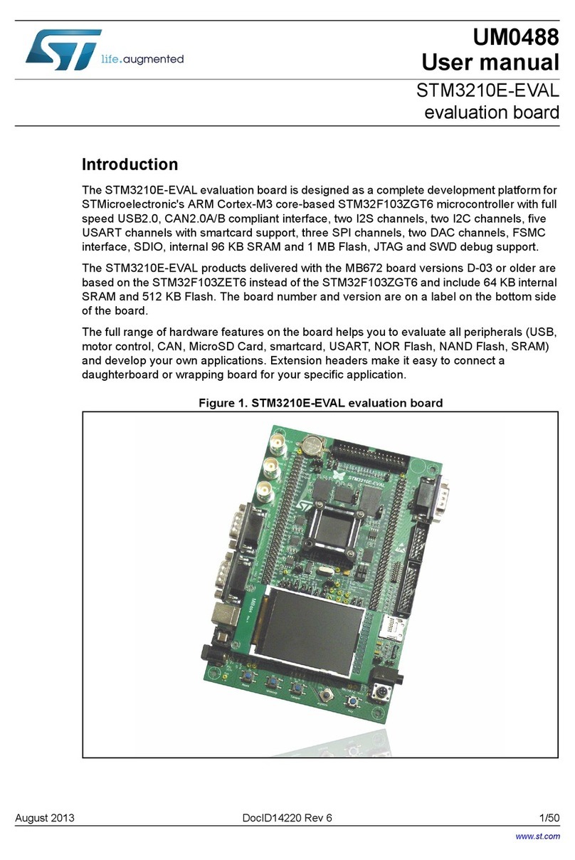
The STM32MP157F-EV1 Evaluation board is designed as a complete demonstration and development platform for
STMicroelectronics Arm®-based dual Cortex®‑A7 32 bits and Cortex®‑M4 32 bits MPUs in the STM32MP1 Series. It leverages
the capabilities of increased-frequency 800 MHz STM32MP1 Series microprocessors for the user to develop applications, using
STM32 MPU OpenSTLinux Distribution software for the main processor, and STM32CubeMP1 software for the co-processor. It
includes an ST-LINK embedded debug tool, LEDs, push-buttons, one joystick, 1-Gbps Ethernet, CAN FD, one USB OTG Micro-
AB connector, four USB Host Type-A connectors, LCD display with touch panel, camera, stereo headset jack with analog
microphone input, four digital microphones, one SPDIF Rx/Tx, smartcard, microSD™ card, and eMMC, NOR and NAND Flash
memories.
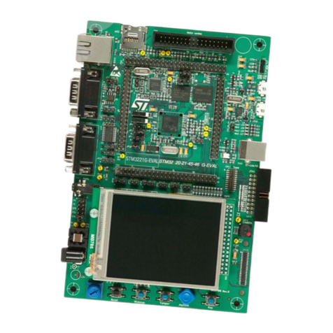
STM32MP157F-EV1, shown in Figure 1 and Figure 2, is used as the reference design for user application development,
although it is not considered as final application.
To expand the functionality of the STM32MP157F-EV1 Evaluation board, two GPIO expansion connectors are also available for
motor control and Raspberry Pi® shields.
An ST-LINK/V2-1 is integrated on the board, as embedded in-circuit debugger and programmer for the STM32 MPU and the
USB Virtual COM port bridge.
Figure 1. STM32MP157F-EV1 top view Figure 2. STM32MP157F-EV1 bottom view
Pictures are not contractual.
Evaluation board with increased-frequency 800 MHz STM32MP157 MPU
UM2648
User manual
UM2648 - Rev 1 - June 2020
For further information contact your local STMicroelectronics sales office. www.st.com

1Features
• STM32MP157 Arm®-based dual Cortex®‑A7 800 MHz 32 bits + Cortex®‑M4 32 bits MPU in LFBGA448
package
• ST PMIC STPMIC1
• 2 × 4-Gbit DDR3L, 16 bits, 533 MHz
• 2 × 512-Mbit Quad-SPI Flash memory
• 32-Gbit eMMC v5.0
• 8-Gbit SLC NAND, 8 bits, 8-bit ECC, 4-KB PS
• 1-Gbit/s Ethernet (RGMII) compliant with IEEE-802.3ab
• USB Host 4-port hub
• USB OTG HS
• CAN FD
• 5.5" TFT 720×1280 pixels with LED backlight, MIPI DSISM interface, and capacitive touch panel
• SAI audio codec
• 5-megapixel, 8-bit camera
• 4 × ST-MEMS digital microphones
• Smartcard
• microSD™ card
• 2 user LEDs
• 2 user and reset push-buttons, 1 wake-up button
• 4-direction joystick with selection button
• 5 V / 4 A power supply
• Board connectors:
– Ethernet RJ45
– 4 × USB Host Type-A
– USB OTG Micro-AB
– SPDIF RCA input and output
– CAN FD
– Stereo headset jack including analog microphone input
– Audio jack for external speakers
– Motor control
– External I2C
– LTDC
– Trace, JTAG, RS-232
– GPIO expansion connector (Raspberry Pi® shields capability)
– MEMS-microphone daughterboard expansion connector
• On-board ST-LINK/V2-1 debugger/programmer with USB re-enumeration capability: Virtual COM port and
debug port
•STM32CubeMP1 and full mainline open-source Linux® STM32 MPU OpenSTLinux Distribution (such as
STM32MP1Starter) software and examples
• Support of a wide choice of Integrated Development Environments (IDEs) including IAR Embedded
Workbench®, MDK-ARM, and STM32CubeIDE
STM32 Arm Cortex MPUs are based on the Arm® Cortex®-A and Cortex®-M processors.
Note: Arm is a registered trademark of Arm Limited (or its subsidiaries) in the US and/or elsewhere.
UM2648
Features
UM2648 - Rev 1 page 2/61

2Ordering information
To order an STM32MP157 Evaluation board, refer to Table 1. Additional information is available from the
datasheet and reference manual of the target STM32.
Table 1. List of available products
Order code Board reference Target STM32 Differentiating
features
STM32MP157F-EV1
• MB1262: mother board
•MB1263: MPU subsystem daughterboard
• MB1230: DSI display board
• MB1379: camera board
STM32MP157FAA1 Secure Boot and
cryptography
2.1 Product marking
Evaluation tools marked as “ES” or “E” are not yet qualified and therefore not ready to be used as reference
design or in production. Any consequences deriving from such usage will not be at ST charge. In no event, ST will
be liable for any customer usage of these engineering sample tools as reference designs or in production.
“E” or “ES” marking examples of location:
•On the targeted STM32 that is soldered on the board (For an illustration of STM32 marking, refer to the
STM32 datasheet “Package information” paragraph at the www.st.com website).
• Next to the evaluation tool ordering part number that is stuck or silk-screen printed on the board.
2.2 Codification
The meaning of the codification is explained in Table 2.
Table 2. Codification explanation
STM32MP1XXY-EVZ Description Example: STM32MP157F-EV1
STM32MP1 MPU series in STM32 Arm Cortex MPUs STM32MP1 Series
XX MPU product line in the series STM32MP157
Y
Options:
•F: Secure Boot, cryptography hardware, 800 MHz
increased frequency
Secure Boot, cryptography hardware,
800 MHz increased frequency
EVZ Evaluation board configuration
•EV1: with PMIC PMIC
The order code is mentioned on a sticker placed on the top or bottom side of the board.
UM2648
Ordering information
UM2648 - Rev 1 page 3/61

3Development environment
3.1 System requirements
• Windows® OS (7, 8 and 10), Linux® 64-bit, or macOS®
•USB Type-C™ to Type-A cable
• USB Type-A to Micro-B cable
• USB Type-A to Micro-AB cable
Note: macOS® is a trademark of Apple Inc. registered in the U.S. and other countries.
3.2 Development toolchains
• IAR Systems - IAR Embedded Workbench®(1)
•Keil® - MDK-ARM(1)
• STMicroelectronics - STM32CubeIDE
• GCC
1. On Windows® only.
3.3 Demonstration software
The STM32 MPU OpenSTLinux Distribution and STM32CubeMP1 base demonstration software is preloaded in
the microSD™ for easy demonstration of the device peripherals in standalone mode. The latest versions of the
demonstration source code and associated documentation can be downloaded from www.st.com.
UM2648
Development environment
UM2648 - Rev 1 page 4/61

4Conventions
Table 3 provides the conventions used for the ON and OFF settings in the present document.
Table 3. ON/OFF convention
Convention Definition
Jumper JPx ON Jumper fitted
Jumper JPx OFF Jumper not fitted
Jumper JPx [1-2] Jumper fitted between Pin 1 and Pin 2
Solder bridge SBx ON SBx connections closed by 0 Ω resistor
Solder bridge SBx OFF SBx connections left open
Resistor Rx ON Resistor soldered
Resistor Rx OFF Resistor not soldered
UM2648
Conventions
UM2648 - Rev 1 page 5/61

5Delivery recommendations
Before the first use, make sure that no damage occurred to the board during shipment and no socketed
components are loose in their sockets or fallen into the plastic bag.
In particular, pay attention to the following components:
1. MB1263 daughterboard connected to the MB1262 mother board
2. microSD card in its MB1263/CN9 receptacle
3. LCD MB1230 daughterboard in MB1262/CN19 DSI connector, and screw, spacer and nut are in place
4. Camera module MB1379 board in MB1262/CN7 connector, and screw, spacer and nut are in place
For product information related to the STM32MP157 microprocessors, visit the www.st.com website.
UM2648
Delivery recommendations
UM2648 - Rev 1 page 6/61

6Hardware layout and configuration
The STM32MP157F-EV1 Evaluation board is designed around the STM32MP157FAA1 target microprocessor in
LFBGA 448-pin package. Figure 3 illustrates the STM32MP157F-EV1 hardware block diagram. Figure 4 shows
the location of main components on the Evaluation board.
UM2648
Hardware layout and configuration
UM2648 - Rev 1 page 7/61

Figure 3. STM32MP157F-EV1 hardware block diagram
STM32MP157xAAx
RTC 32 kHz crystal
Capacitive
touch screen
USB OTG Micro-AB USB
OTG HS
5.5" TFT 720x1280
USB
Host HS
USB Hub
4x USB Type-A
microSD™ card
connector
SDMMC
HSI
I2C
GPIO
2 user LEDs
2 user buttons
1 reset button
Smartcard
connector
Smartcard
SAI Audio codec
STPMIC1
5V_VIN
24 MHz crystal
GPIO 40-pin
connector
GPIOs
DDR3L DDR
LTDC LTDC connector
DSI
eMMC SDMMC
NAND FMC
Quad-SPI NOR
Flash Quad-SPI
Gigabit Ethernet RGMII DFSDM MEMS microphones
SPDIF
Tx/Rx SPDIF Tx/Rx
DCMI Camera
CAN FDCAN FD connector
UART
RS-232 DB9
connector
JTAG/
SWD
ST-LINK/V2-1
USB Micro-B
Motor-control
connector
Shared
GPIOs
I2C
ADC/DAC ADC/DAC
connector
MICTOR-38
connector ETM
JTAG connector
Wake-up button
MFX I/O expander
Joystick
Stereo Jack
Line Out / MIC_IN
I2CI2C_EXT connector
UM2648
Hardware layout and configuration
UM2648 - Rev 1 page 8/61

Table 4. STM32MP157F-EV1 overview
Position Description
1 MB1262 mother board
2 MB1263 daughterboard
3MB1230 DSI (MIPI® standard) 720p display
4 MB1379 daughterboard camera
5microSD™ card
Table 5. MB1263 daughterboard overview
Position Description Position Description
50 (B1) Reset button 59 (CN1) MB1263 power 5 V-3 A
51 (LD2) User LED (red) 60 (SW1) Boot mode selection
52 (B2) User button (PA13) 61 (U3) PMIC (STPMIC1A)
53 (LD3) User LED (green) 62 (LD6) ST-LINK LED (bicolor)
54 (B3) User button (PA14) 63 (CN4) USB Micro-B (ST-LINK/V2-1)
55 (LD5) User LED (blue) 64 (U4) STM32MP157FAA1 LFBGA448
56 (LD4) User LED (orange) 65 (U5) eMMC
57 (B4) Wake-up button 66 (U6/U7) 2 x DDR3L 16 bits
58 (LD1) Power LED (green) 67 (µSD)microSD™ 3.0 card (back side slot)
Table 6. MB1262 mother board overview
Position Description Position Description
10 (CN3) Ethernet 11 (CN8) Microphone MEMS daughterboard connector
12 (CN4) Speaker audio output 13 (CN5) Headset audio output
14 (U8) Audio codec (Wolfson WM8994) 15 (CN1) SPDIF RX
16 (CN2) SPDIF TX 17 (U5) Smartcard (back side slot)
18 (LD1) Ethernet LED (green) 19 (CN6) Ethernet daughterboard connector
20 (U10) Trace connector 21 (CN11)LTDC LCD TFT display controller (STM32
specific) connector
22 (CN12) RS-232 (UART4) 23 (CN13) External E2P connector
24 (CN16) USB Micro-AB (USB OTG) 25 (LD2) USB OTG LED (green)
26 (LD3) USB Type-A port LED (red) 27 (CN17) MFX header 4 pins
28 (CN14) JTAG connector 29 (CN15) CAN FD
30 (CN18) 2 USB Type-A port (host) 31 (CN20) 2 USB Type-A port (host)
32 (B2) Reset button 33 (B1) Joystick
34 (CN22) Motor control connector 35 (CN21) GPIO expansion connector
4 (CN7) Camera sensor connector - -
UM2648
Hardware layout and configuration
UM2648 - Rev 1 page 10/61
6.1 Power supply management
6.1.1 5 V power supply
STM32MP157F-EV1 Evaluation board is designed to be powered from the 5 V DC power supply provided in the
package.
MB1263/LD1 Green LED turns on when this power supply is connected to the power jack MB1263/CN1.
Figure 5. 5 V power supply connector: MB1263/CN1
6.1.2 Platform power tree
All supply lines required for the operation of the components on STM32MP157F-EV1 are derived from the 5 V
power source. Indeed, this 5 V power source is the input supply of the STPMIC1 that distributes then all the
supplies to the subsystems as described in the power tree Figure 6.
The voltage on the VBAT pin of the STM32MP157FAA1 can be provided by an external battery. Use MB1263/BT1
to plug a CR1220 3 V lithium battery. Table 7 describes the HW configuration for the VBAT connection.
Table 7. HW configuration for the VBAT connection
Jumpers Setting Configuration(1)
MB1263/JP3 JP3[1-2] VBAT connected to VDD
JP3[2-3] VBAT connected to CR1220 battery holder MB1263/BT1
1. Default configuration in bold
UM2648
Power supply management
UM2648 - Rev 1 page 11/61

Figure 6. STM32MP157F-EV1platform power tree
STM32MP157xAAx
VDD
VDDCORE
VDDQ_DDR
DDR_VREF
VDDA
VDD_OTP
VDD_DSI
BYPASS_REG1V8
VDDA1V8_REG
VDDA1V8_DSI
PDR_ON
PDR_ON_CORE
NRST_CORE
VDD1V2_DSI_REG
VDD1V2_DSI_PHY
VDD3V3_USBHS
VDDA1V1_REG
VBAT
VDD3V3_USBFS
PA0 (WKUP1)
PZ4 (I2C4_SCL)
PZ5 (I2C4_SDA)
PWR_ON
NRST
PC13 (RTC_OUT1)
VDD_PLL
VREF+
VREF-
VSSA
VDD_ANA
DDR3 x16
2x DDR3L
VDD
VDDQ
VREFCA
VREFDQ
termination
4Gb / 16-bits /
1066Mbps
VTT_DDR (0.675 V)
VDD_DDR (1.35 V)
VREF_DDR (0.675 V)
VDDCORE (1.2 V)
VDD (3.3 V)
BUCK1
0.725-1.5 V,1.5 A
BUCK1IN
VLX1
VOUT1
1uH
22uF
BUCK2
BUCK2IN
VLX2
VOUT2
1uH
22uF
BUCK3
1.0-3.4 V, 0.5 A
BUCK3IN
VLX3
VOUT3
22uF
LDO1
1.7-3.3V,350mA
LDO16IN LDO1OUT
4.7uF
LDO2
1.7-3.3V,350mA
LDO25IN LDO2OUT
LDO3IN LDO3OUT
10uF
LDO4
3.3V,50mA
VIN LDO4OUT
LDO5
1.7-3.9V,400mA LDO5OUT
LDO6
0.9-3.3V,100mA LDO6OUT
BOOST (5 V)
5.2 V,1 A BOUT
VREF VREF
1uF
Logic / Control
VDD
PONKEY
5V DC
3A
WAKEUP
SCL
SDA
PWREN
INT1
VBUSOT
G
RSTn
VBUSOTG_SW 0.5 A
(w/ OCP and VBUSdet)
LDO3
VLXB1
1uH
BUCK4
0.6-3.9V,2A
BUCK4IN
VLX4
VOUT4
22uF
Vin_max
PWR
MUX
INTLDO INTLDO
BYPASS_SW
PWR_SW 1 A
(w/ OCP and VBUSdet) SWOUT
SWIN VBUS_SW
22uF
10uF
10uF
10uF
10uF
1uH
1uH
10uF
220uF
10uF
1uF
1uF
4.7uF
4.7uF
4.7uF
4.7uF
4.7uF
4.7uF
STPMIC1
VDDA
VBUS_OTG
VDD_USB (3.3 V)
3V3
VDD_SD (2.9V)
VDD
microSD card
3V3
POWER JACK
MB1263
MB1262
2x High Speed Connectors
3V3
VDD
VIN
VIN
3V3
1V8
VBUS_OTG
1V8
2V8
2V8 MotorC
conn.
Smartcard
GPIO
40-pin conn.
Camera
DSI
LCD
Gigabit
Ethernet
SN65HVD230
CAN FD
RS-232
JTAG &
Trace
connectors
Audio
codec
x4 MEMS
micro
SPDIF
USB Host
Type-A x4
WAKE-UP
PUSH
BUTTON
NAND VCC
Q-SPI NOR VCC
Micro-AB
USB OTG
Protection
LC
LowPass
VIN TYPE-µB
Embedded STLINK V2.1
MFX I/O expander
4.7uF
VBUS
BST_OUT
eMMC
3V3
VDD VCCQ
VCC
PWR_LP
NC
VIO
VDD_DDR
RESET
PUSH
BUTTON
VBUS_SW
6.1.3 STPMIC1
For general information concerning the STPMIC1, please refer to STPMIC1 datasheet at the www.st.com website.
UM2648
Power supply management
UM2648 - Rev 1 page 12/61

6.2 Clocks
Two clocks are available on STM32MP157F-EV1 for the STM32MP157FAA1 target microprocessor.
6.2.1 LSE clock
• External 32.768 kHz crystal
6.2.2 HSE clock
• External 24 MHz crystal
6.3 Reset sources
The reset signal of the STM32MP157F-EV1 platform is active low.
The sources of the platform reset are:
•Two reset buttons MB1263/B1 and MB1262/B2 (black buttons)
• STM32MP157FAA1 microprocessor: internal voltage monitor, SW request or watchdog
• STPMIC1
• JTAG/SWD connector MB1262/CN14
• ETM Trace Mictor-38 connector MB1262/U10
• Embedded ST-LINK/V2-1
The STM32MP157FAA1 microprocessor also drives a subsystem reset, SUB_NRST signal on PD10 IO, to the
peripherals: USB Host Hub, MFX, Ethernet, and RGB_LTDC connector.
6.4 User buttons and LEDs
Table 8 describes the HW configuration for the user buttons and LEDs.
Table 8. HW configuration for the user buttons and LEDs
I/O LED color and label Button label
PD8 PD8 is connected to the orange LD4. Active High -
PD9 PD9 is connected to the blue LD5. Active High -
PA13 PA13 is connected to red LD2. Active Low User PA13
PA14 MFX_IO13 is connected to orange LED LD7. Active Low User PA14
6.5 Physical input devices: buttons
The STM32MP157F-EV1 board provides a number of input devices for physical human control:
•Two reset buttons (MB1263/B1 and MB1262/B2)
• Four-way joystick controller with select key (MB1262/B1)
• Wake-up button (MB1263/B4)
Table 9. Physical user devices: buttons
Devices Purpose - I/O
Wake-up button (MB1263/B4)
Awakes the platform from low-power modes.
Connected to STPMIC1 PONKEY, which
generates a wake-up signal on STM32MP157
PA0
Reset buttons (MB1263/B1 or MB1262/B2) NRST signal
JOY_CENTER: Joystick select key (MB1262/B1 pin2) MFX_IO0
JOY_DOWN: Joystick down direction (MB1262/B1 pin3) MFX_IO1
UM2648
Clocks
UM2648 - Rev 1 page 13/61

Devices Purpose - I/O
JOY_LEFT: Joystick left direction (MB1262/B1 pin1) MFX_IO2
JOY_RIGHT: Joystick right direction (MB1262/B1 pin6) MFX_IO3
JOY_UP: Joystick up direction (MB1262/B1 pin4) MFX_IO4
6.6 Boot options
The STM32MP157x-EV1 board may boot from different sources as described in Table 10.
Table 10. HW configuration for the boot mode MB1263/SW1
Boot mode BOOT2 BOOT1 BOOT0
Serial NOR 0 0 1
microSD card 1 0 1
eMMC 0 1 0
NAND 0 1 1
UART and USB 000
110
Reserved 1 0 0
The boot related switches (MB1263/SW1) must be configured as illustrated by one of the following pictures:
UM2648
Boot options
UM2648 - Rev 1 page 14/61

Figure 7. STM32MP157F-EV1 boot-related switch configuration
6.7 Embedded ST-LINK/V2-1
The ST-LINK/V2-1 programming and debugging tool is integrated in the STM32MP157F-EV1 Evaluation board.
The embedded ST-LINK/V2-1 supports JTAG, SWD and VCP for the target STM32 Arm Cortex MPUs.
UM2648
Embedded ST-LINK/V2-1
UM2648 - Rev 1 page 15/61

For information about debugging and programming features refer to the ST-LINK/V2 in-circuit debugger/
programmer for STM8 and STM32 user manual (UM1075) available on www.st.com, which describes in details all
the ST-LINK/V2-1 features.
Figure 8 shows the ST-LINK USB Micro-B connector pinout.
Figure 8. ST-LINK USB Micro-B connector pinout MB1263/CN4
Table 11 describes the ST-LINK USB Micro-B connector pinout.
Table 11. ST-LINK USB Micro-B connector pinout MB1263/CN4
Pin Board function ST-LINK STM32 pin
1 VBUS Power -
2 DM PA11
3 DP PA12
4 ID GND
5 GND GND
Since the current consumption of the STM32MP157F-EV1 Evaluation board exceeds the permissible current on
the USB, it is not possible to power the board through the ST-LINK/V2-1 USB. To use the ST-LINK/V2-1 for
programming and debugging, it is mandatory to power the board first using the 5 V power supply, then connect
the ST-LINK/V2-1 USB cable to the PC. Proceeding this way, the USB enumeration succeeds with the support of
the external power source.
The user must respect the following power sequence procedure:
1. Check that MB1263/JP1 is OFF, MB1263/JP4 [2-3] and JP5 [2-3] are ON to connect UART4 as ST-
LINK VCP.
2. Connect the 5 V power source, MB1263/LD1 LED turns green, MB1263/LD6 LED flashes red.
3. Connect the PC to USB connector MB1263/CN4, MB1263/LD6 LED is red and becomes green once the
connection with the ST-LINK is established.
6.7.1 Drivers
The ST-LINK/V2-1 requires a dedicated USB driver, which, for Windows 7®, Windows 8® and Windows 10®, is
found at www.st.com.
In case the STM32MP157F-EV1 Evaluation board is connected to the PC before the driver is installed, some of
its interfaces may be declared as “Unknown” in the PC device manager. In this case, the user must install the
dedicated driver files, and update the driver of the connected device from the device manager as shown in
Figure 9.
Note: Prefer using the USB Composite Device handle for a full recovery.
UM2648
Embedded ST-LINK/V2-1
UM2648 - Rev 1 page 16/61

Figure 9. USB composite device
6.7.2 ST-LINK/V2-1 firmware upgrade
For its own operation, ST-LINK/V2-1 embeds a dedicated microcontroller with Flash memory. Its firmware
determines ST-LINK/V2-1 functionality and performance.
The ST-LINK/V2-1 embeds a firmware mechanism for the in-situ upgrade through the USB port. As the firmware
may evolve during the lifespan of the ST-LINK/V2-1 product (for example new functionalities, bug fixes, support
for new microcontroller families), it is recommended to visit the www.st.com website before starting to use the
STM32MP157F-EV1 Evaluation board and periodically, to stay up-to-date with the latest firmware version.
6.8 ETM TRACE Mictor-38 connector
The Mictor-38 connector MB1262/U10 may output trace signals used for debug, as well as JTAG signals.
Table 12 describes the HW configuration for the TRACE function.
Table 12. HW configuration for the TRACE connector MB1262/U10
I/O Bridge Setting(1) Comment
PI14 SB38
ON PI14 may be used for the trace function TRACE CLK
OFF PI14 is not connected to Trace
PI14 may be used for LTDC CLK
PI12 SB43
ON PI12 may be used for the trace function TRACE_D0
OFF PI12 is not connected to Trace
PI12 may be used for LTDC HSYNC
PI13 SB42
ON PI13 may be used for the trace function TRACE_D1
OFF PI13 is not connected to Trace
PI13 may be used for LTDC VSYNC
PJ5 SB36
ON PJ5 may be used for the trace function TRACE_D2
OFF PJ5 is not connected to Trace
PJ5 may be used forLTDC_R6
PJ6 SB41
ON PJ6 be used for the trace function TRACE_D3
OFF PJ6 is not connected to Trace
PJ6 may be used for LTDC_R7
PK1 SB40 ON PK1 may be used for the trace function TRACE_D4
UM2648
ETM TRACE Mictor-38 connector
UM2648 - Rev 1 page 17/61

I/O Bridge Setting(1) Comment
PK1 SB40 OFF PK1 is not connected to Trace
PK1 may be used for LTDC_G6
PK2 SB39
ON PK2 may be used for the trace function TRACE_D5
OFF PK2 is not connected to Trace
PK2 may be used for LTDC_G7
PK5 SB49
ON PK5 may be used for the trace function TRACE_D6
OFF PK5 is not connected to Trace
PK5 may be used for LTDC_B6
PK6 SB35
ON PK6 may be used for the trace function TRACE_D7
OFF PK6 is not connected to Trace
PK6 may be used for LTDC_B7
PJ0 SB34
ON PJ0 may be used for the trace function TRACE_D8
OFF PJ0 is not connected to Trace
PJ0 may be used for LTDC_R1
PJ1 SB37
ON PJ1 may be used for the trace function TRACE_D9
OFF PJ1 is not connected to Trace
PJ1 may be used for LTDC_R2
PJ2 SB48
ON PJ2 may be used for the trace function TRACE_D10
OFF PJ2 is not connected to Trace
PJ2 may be used for LTDC_R3
PJ3 SB47
ON PJ3 may be used for the trace function TRACE_D11
OFF PJ3 is not connected to Trace
PJ3 may be used for LTDC_R4
PJ4 SB46
ON PJ4 may be used for the trace function TRACE_D12
OFF PJ4 is not connected to Trace
PJ4 may be used for LTDC_R5
PJ7 SB45
ON PJ7 may be used for the trace function TRACE_D13
OFF PJ7 is not connected to Trace
PJ7 may be used for LTDC_G0
PJ8 SB44
ON PJ8 may be used for the trace function TRACE_D14
OFF PJ8 is not connected to Trace
PJ8 may be used for LTDC_G1
PJ9 SB50
ON PJ9 may be used for the trace function TRACE_D15
OFF PJ9 is not connected to Trace
PJ9 may be used for LTDC_G2
1. Default configuration is shown in bold
Figure 10 shows the TRACE Mictor-38 connector
UM2648
ETM TRACE Mictor-38 connector
UM2648 - Rev 1 page 18/61

Figure 10. TRACE Mictor-38 connector: MB1262/U10
Table 13 describes the MICTOR-38 connector pinout for TRACE and JTAG signals.
Table 13. TRACE MICTOR-38 connector pinout: MB1262/U10
Board function Pin Pin Board function
NC 1 2 NC
NC 3 4 NC
GND 5 6 TRACE_CLK
Pull-down 7 8 Pull-down
NRST 9 10 Pull-down
TDO/SWO 11 12 VDD
Pulldown 13 14 VDD
TCK/SWCLK 15 16 TRACE_D7
TMS/SWDIO 17 18 TRACE_D6
TDI 19 20 TRACE_D5
NJTRST 21 22 TRACE_D4
TRACE_D15 23 24 TRACE_D3
TRACE_D14 25 26 TRACE_D2
TRACE_D13 27 28 TRACE_D1
TRACE_D12 29 30 GND
TRACE_D11 31 32 GND
TRACE_D10 33 34 VDD
TRACE_D9 35 36 GND
TRACE_D8 37 38 TRACE_D0
6.9 JTAG connector
A JTAG/Serial Wire Debug 20-pin IDC connector (ARM JTAG 20, IDC 2.54 mm) MB1262/CN14 outputs the JTAG
signals. The JTAG function is a dedicated interface of the STM32MP157FAA1 microprocessor.
Table 14 describes the JTAG connector pinout.
UM2648
JTAG connector
UM2648 - Rev 1 page 19/61

Table 14. MB1262/CN14 JTAG connector pinout
Board function Pin Pin Board function
Power 1 2 Power
NJTRST 3 4 GND
JTDI 5 6 GND
JTMS/SWDIO 7 8 GND
JTCK/SWCLK 9 10 GND
Pull down 11 12 GND
JTDO/SWO 13 14 GND
NRST 15 16 GND
Pull down 17 18 GND
Pull down 19 20 GND
6.10 DDR3L
Two 16-bit DDR3L NT5CC256M16ER-EK of 4 Gbytes are implemented in flyby topology in MB1263/U6 and U7
positions. They are connected to the dedicated DDR interface of STM32MP157FAA1. For detailed information
concerning the DDR HW design implementation, refer to the application note AN5122 available on the
www.st.com website.
6.11 eMMC
The STM32MP157FAA1 SDMMC2 in 8-bit wide bus mode drives a THGBMNG5D1LBAIL 32-Gbit eMMC in
MB1263/U5 position.
6.11.1 eMMC I/O interface
Table 15 describes the HW configuration for the eMMC interface.
Table 15. HW configuration for the eMMC interface
I/O Configuration(1)
PB14 SDMMC2_D0 connected to MB1263/U5 DAT0
PB15 SDMMC2_D1 connected to MB1263/U5 DAT1
PB3 SDMMC2_D2 connected to MB1263/U5 DAT2
PB4 SDMMC2_D3 connected to MB1263/U5 DAT3
PA8 SDMMC2_D4 connected to MB1263/U5 DAT4
PA9 SDMMC2_D5 connected to MB1263/U5 DAT5
PE5 SDMMC2_D6 connected to MB1263/U5 DAT6
PD3 SDMMC2_D7 connected to MB1263/U5 DAT7
PE3 SDMMC2_CK connected to MB1263/U5 CLK
PG6 SDMMC2_CMD connected to MB1263/U5 CMD
1. Minimum set of signals required by the boot ROM during eMMC boot in bold
6.12 NAND Flash memory
The STM32MP157FAA1 FMC interface is connected to an 8-Gbit SLC NAND, 8-bit, 8-bit ECC, and 4-KByte PS
MT29F8G08ABACAH4 in MB1262/U11 position.
UM2648
DDR3L
UM2648 - Rev 1 page 20/61
Table of contents
Other ST Motherboard manuals

ST
ST SPC560D-DIS User manual

ST
ST STSW-S2LP-KNX-DK User manual

ST
ST EVAL-L9963E-MCU User manual

ST
ST STM32F746G-DISCO User manual

ST
ST UM2313 User manual

ST
ST STEVAL-LLL011V1 User manual

ST
ST STEVAL-SPIN3202 User manual

ST
ST STM8T141-EVAL User manual

ST
ST STM32F401 Discovery User manual

ST
ST B-L4S5I-IOT01A User manual

ST
ST STEVAL-ICB008V1 User manual

ST
ST STEVAL-IDB007V1 User manual

ST
ST ST25DV-I2C User manual

ST
ST STM32MP157 Series User manual

ST
ST STEVAL-BLUEPIRV1 User manual

ST
ST AEKD-USBTYPEC1 User manual

ST
ST STEVAL-MKI005V1 User manual

ST
ST STEVAL-IDB011V1 User manual

ST
ST STEVAL-PCC001V1 User manual

ST
ST STM32439I-EVAL User manual