2.2.4 Bus voltage sensing circuit
The STEVAL-SPIN3202 evaluation board provides the bus voltage sensing. This signal is
set through a voltage divider by the motor supply voltage (VBUS, R10 and R16) and sent to
the PB1 GPIO (the ADC channel 9) of the embedded MCU. The signal is also available on
the TP6.
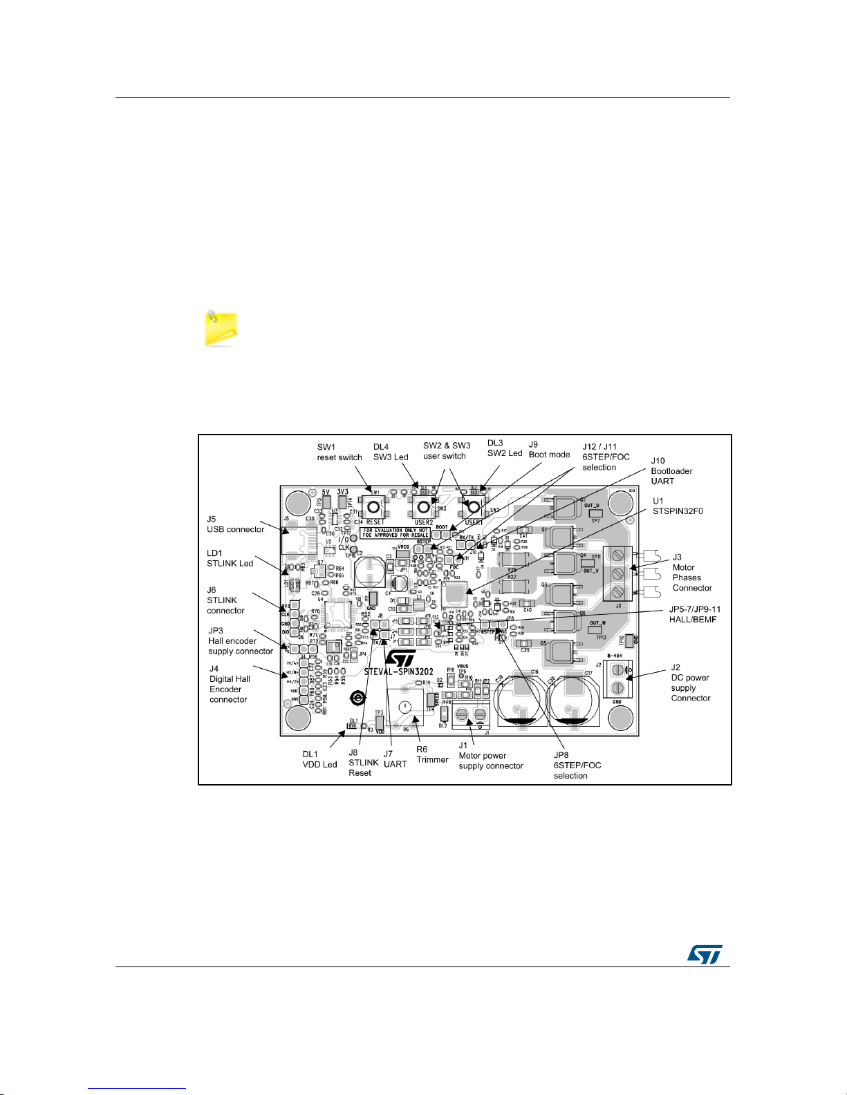
2.2.5 Hardware user interface
The board provides the following hardware user interface:
potentiometer (R6 setting, for example, the target speed)
switch SW1 (to reset STSPIN32F0A MCU and ST-LINK V2)
switch SW2 (user button 1)
Switch SW3 (user button 2)
LED DL3 (user LED 1, turned on when the user 1 button is pressed too)
LED DL4 (user LED 2, turned on when the user 2 button is pressed too)
2.2.6 Debug
The STEVAL-SPIN3202 evaluation board embeds an ST-LINK/V2-1
debugger/programmer.
The ST-LINK features:
USB software re-enumeration
virtual com port interface on USB connected to the STSPIN32F0A (UART1) PB6/PB7
pins
mass storage interface on USB
The ST-LINK is supplied by the host PC through the USB cable connected to the board.
The LED LD1 provides ST-LINK communication status information:
Red LED flashing slowly: at power-on before USB initialization
Red LED flashing quickly: following the first successful communication between the
PC and ST-LINK/V2-1 (enumeration)
Red LED ON: the initialization between the PC and ST-LINK/V2-1 is complete
Green LED ON: successful target communication initialization
Red/green LED flashing: during communication with target
Green ON: communication successfully completed
The reset function is activated by removing the jumper J8.