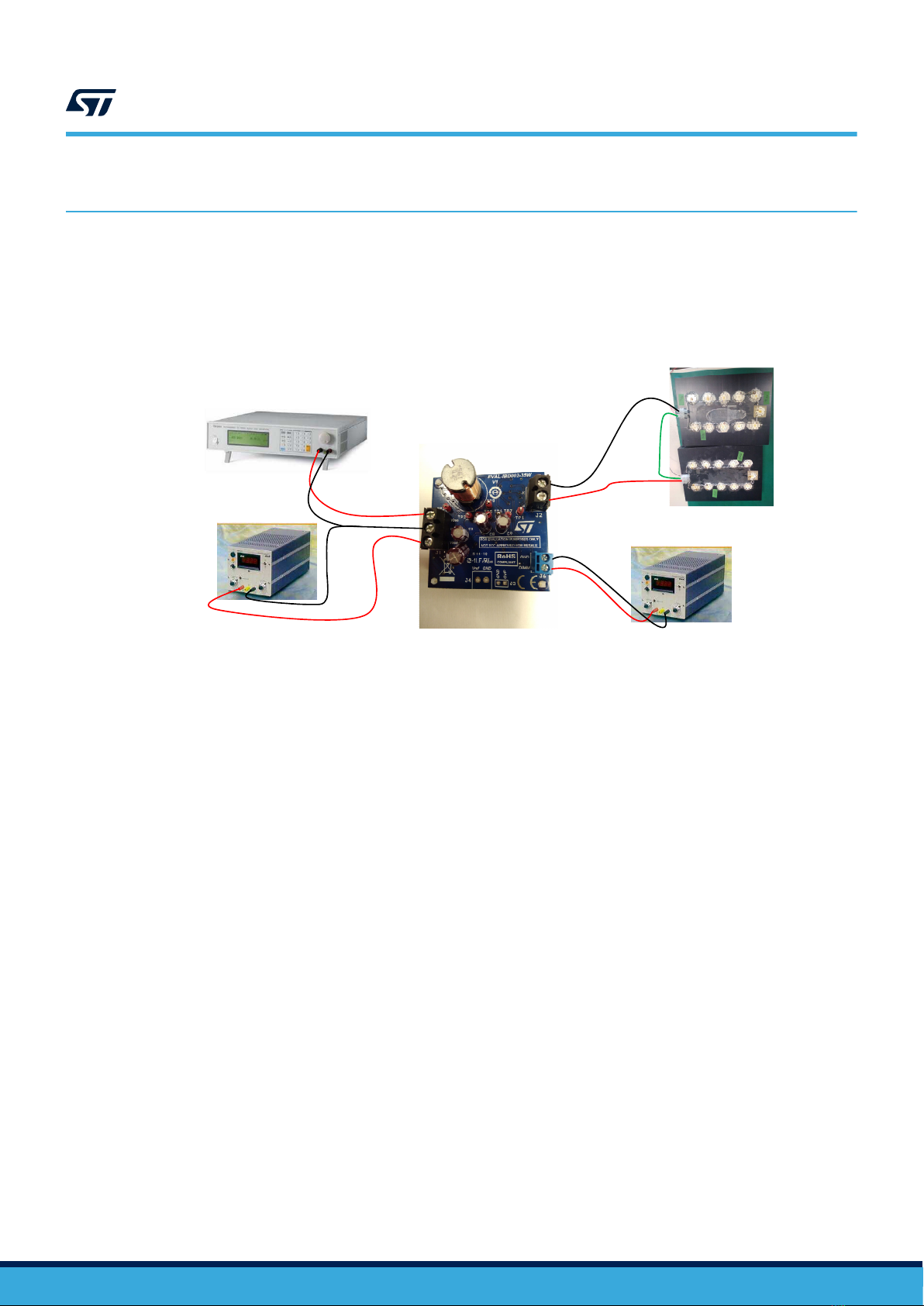
ST EVAL-IBD002-35W User manual

Introduction
This document describes the EVAL-IBD002-35W demonstration board behavior, designed to manage a dimmable 35 W LED
load with a single inverse buck stage.
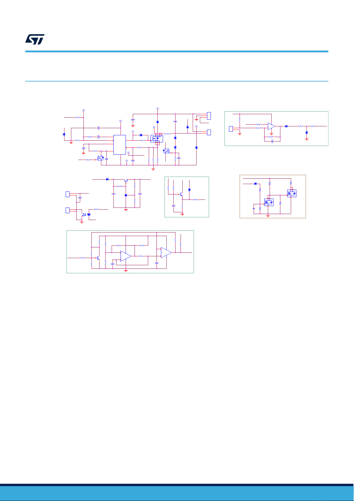
The HVLED002 controller manages the inverse buck circuit mainly composed by D1, L1 and Q1 components. This circuit
provides around 700 mA as maximum LED load current. The board operates in peak current mode with FOT (Fixed Off Time)
and it has been designed to operate with wide input (48 V - 60 V) and wide output (24 V - 48 V) voltages. The on-time changes
according to the operating condition to keep output current regulated and the switching frequency is consequently adapted.
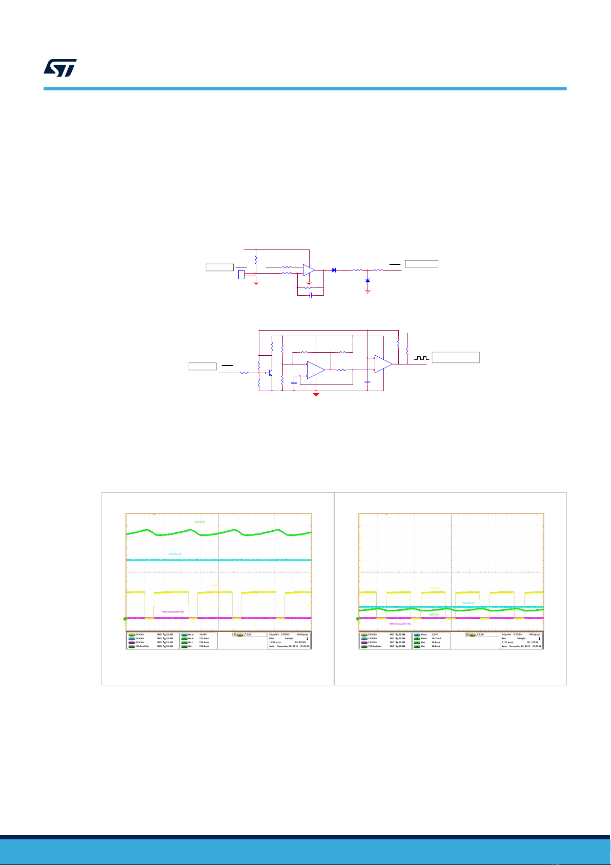
In steady-state condition the pin COMP works at its maximum value because the FB signal is zero, providing the maximum
average current.. In this condition, decreasing VDimm input below 10 V, the Analog dimming circuit injects an ever higher offset
signal on HVLED002 current sense, so decreasing the output average current. When VDimm input voltage decreases under 2
V, the PWM Dimming circuit starts to generate a PWM output voltage with 5 V - 0 V amplitude. When PWM state is 0 V the FB
signal is zero providing the maximum average current and when the PWM state is 5 V the pin FB is pulled up to VREF and the
switching activity of HVLED002 is stopped providing zero output current. In this way, when the Vdimm is under 2 V, the output
average current increases/decreases depending on the PWM state condition. . Decreasing VDimm voltage level, the PWM high
level percentage increases, further decreasing the output average current too. So, the external 0 -10 V dimming signal is
dedicated to managing a dimmed output LED current between 1%-100% of its maximum value with both Analog control
100%÷10% (10 V÷2 V) and PWM control 10%÷1% (2 V÷0 V).
An external 15 Vdc of auxiliary voltage is needed to power up the HVLED002 controller while the D6, Q3 and U2 components
regulate a precise 12 V to the Vcc of HVLED002 and manage a constant pull-up voltage used for both dimming circuits.
The short-circuit protection is guaranteed by Zener diode D10 which detects a sudden fast slope rise of LED load Cathode
Voltage activating Q6 MOSFET and bringing the pin FB high and stopping the switching activity. On the PCB there are also
available (not mounted) the Discharge and OVP circuit positions, usable and useful with a primary stage connection (converter):
the first needed to discharge the C2 output capacitance after power turn-off and the second to stop the primary activity when an
Overvoltage occurs on the Output LED load.
Inverse buck 35W with LED current controlled by HVLED002 with Analog/PWM
dimming regulation
UM2683
User manual
UM2683 - Rev 1 - August 2020
For further information contact your local STMicroelectronics sales office.
www.st.com

1EVAL-IBD002-35W schematic diagrams
Figure 1. EVAL-IBD002-35W circuit schematic
Vled compe ns a tion
Option a l
Vbus=48Vdc-60Vdc
Vaux=15Vdc
Vout=24Vdc-48Vdc
A
K
Vbus
GND
Vaux
PWM Dimming p ortion
Analog Dimming portion
Disc harge
PCB=> CB1 3 .PR1
NM => No t Mo u n te d
35W Inverse Buck with Mixed Dimming
NM
NM
NM
NM NM
NM NM
NM
CS
GD_B
VREF
GD_B
COMP
12Vcc
VFB
Vcc_unre g
RT/CT
PWM
COMP
12Vcc
GD_B
RT/CT
VREF
CS _FLT
VREF
OVP
OVP
VREF
Vcc_unre g
Vbus
VREF
VFB
12Vcc
VK
PWM
VREF12Vcc
DIM
VREF
12Vcc
CS _FLT
DIM
Vbus
Vcc_unre g
Vbus
Pha s e
C5
100nF
Q1
STL4N10F 7
C4
NM
R56
100K
R17
120k
R24
470k
R6
200k
R19
220k
J2
LED
1
2
R57
1K
R28
100k
R26
43k
D9
SZMM3Z6V2T1G
C16
1uF
D2
BZT52C 47 S NM
R4
100R
J5
OVP_dis
1
2
R1
0R0
TP3
NM
TP6
NM
R35
100K
TP4
NM
TP5
NM
C9
10uF
35V
L1
560uH ELC12 D56 1E
D11
1N4148WS
TP7
NM
R7
NM
1%
R20
4.99k
C11
2.2 uF NM
D3
BZX84J -C5 V6
C15
47n
R29
3k3
C8
10uF
35V
C3
100nF TP 2
NM
R61
33K
C2
4.7 uF
100V
TP8
NM
R30
100k
R36
1M
R21
27k
R5
1k D5
STPS2H100AF
U5A LM293S T
3+
2-
8
V+
4
V-
1
OUT
D4
1N4148WS
R31
220k
D22
1N4148WS NM
R16
470k
R11
NM
R32
10k
Q2
2N7002
TP1
NM
Q7A
STL20DN10 F7
2
71
8
U5B LM293S T
5+
6-
8
V+
4
V-
7
OUT
R22
470k
R13
2k7
R33
100k
Q6
2N7002
R2
NM
R15
7.5 k
Q7B
STL20DN10 F7
4
53
6
J4
5V_Out
1
2
U3
TCLT100 7 NM
12
43
U1
HVLED002
VREF
8
OUT 6
VCC 7
GND
5
RT/CT
4
VFB
2
COMP
1
ISENSE 3
R12
100k
R18
200k
C6
470pF
C7
470pF
D1
STPS2H100AF
C1
10uF
100V
R25
150k
J6
0_10 Dim
1
2
D6
1N4148WS
D10
SMZJ3804 B-E3 /52
R54
0R0
C10
10nF
R23
430k
R14
442k
R27
2.2 k NM
R34
2k2
D8
1N4148WS
U2
TL432AIL3T
R55
1M
C14
4n7
Q3
BC817-25L
D7
1N4148WS
R8
0R68
1%
R9
0R62
1%
R10
1k
J1
VIN
1
2
3
C31
1uF
-
+
U4
TS321
4
1
52
3
R3
100k
Q5
BC847
Q4
BC817-25L
C12
10nF
UM2683
EVAL-IBD002-35W schematic diagrams
UM2683 - Rev 1 page 2/24

2EVAL-IBD002-35W demonstration board layout
Figure 2. EVAL-IBD002-35W component side
UM2683
EVAL-IBD002-35W demonstration board layout
UM2683 - Rev 1 page 3/24

Figure 3. EVAL-IBD002-35W solder side
UM2683
EVAL-IBD002-35W demonstration board layout
UM2683 - Rev 1 page 4/24

3EVAL-IBD002-35W demonstration board overview
The main specifications of the EVAL-IBD002-35W power board can be seen below.
Table 1. EVAL-IBD002-35W specification
Parameter Specs
Vin at J1 Connector (Vbus) 48Vdc ÷ 60Vdc
Vout at J6 Connector (Vout A-K) 24Vdc ÷ 48Vdc
Vaux at J1 Connector (Vaux) 15Vdc
Iout Led max. (J2) 700mA
Dimming range 1% ÷ 100%
No load consumption 50mW
Pout max. 35W
Efficiency Full Load: 97%
Load Over 20% (analog dimming): > 95%
Output ripple current max. <80mA@worst case 50Vindc-48Voutdc
Short-circuit protection OK
RoHS compliant OK
Table 2 shows a Legend of all connector and Test Point available on the EVAL-IBD002-35W demonstration board
Table 2. EVAL-IBD002-35W Connectors and Test Point description
Reference Type Specs
J1 PCB terminal Vbus - GND
J1 PCB terminal Vaux - GND
J2 PCB terminal Output A/K LED load
J4 PCB terminal 5v_Out – VREF - Not mounted
J5 PCB terminal OVP_dis - Not mounted
J6 PCB terminal VDIMM - GND
TP1 Test Point Vbus - Not mounted
TP2 Test Point VKathode - Not mounted
TP3 Test Point VGS - Not mounted
TP4 Test Point VDS - Not mounted
TP5 Test Point VCS - Not mounted
TP6 Test Point GND - Not mounted
TP7 Test Point VCC - Not mounted
TP8 Test Point VFB - Not mounted
UM2683
EVAL-IBD002-35W demonstration board overview
UM2683 - Rev 1 page 5/24

4EVAL-IBD002-35W measurement
Figure 4 shows the efficiency measured covering the whole dimming range (1%-100%), supplying the
demonstration board with 60 Vdc (15 Vdc as Auxiliary Voltage) with three different LED loads of 48 V(16LED), 45
V(15LED) and 24 V (8LED), while Figure 5 shows the efficiency measurement with a different input voltage of 48
Vdc and 50 Vdc. In both cases the Efficiency is 97% in Full Load conditions of 35 W (48 Vout-16LED) and higher
than the 95% for Load over the 20% of its maximum Load.
Figure 4. EVAL-IBD002-35W Efficiency vs. dimming@60Vindc
Figure 5. EVAL-IBD002-35W Efficiency vs. dimming@48/50Vindc
UM2683
EVAL-IBD002-35W measurement
UM2683 - Rev 1 page 6/24

5EVAL-IBD002-35W set-up
Figure 6 here below shows a typical set-up, an example of the equipment needed to turn on the EVAL-
IBD002-35W and how/where to connect each one of them.
Figure 6. EVAL-IBD002-35W demonstration board
Power Supply Vdc n.1 (15Vdc)
Power Supply Vdc n.3 (60Vdc)
Led Load
K Load
A Load
EVAL-IBD002-35W
Vbus
Auxiliary Voltage Dimming
Power Supply n.2 (0Vdc÷10Vdc)
Here below a brief guide list to switch on the EVAL-IBD002-35W demonstration board:
• Set the voltage of the Power Supply n.1 to 15 Vdc and from OFF conditions connect it to J1 with (+) to Vaux
and (-) to GND;
• Set the voltage of the Power Supply n.2 to 10 Vdc and from OFF conditions connect it to J6 with (+) to DIMM
and (-) to GND;
• Set the voltage of the Power Supply n.3 to 60 Vdc and from OFF conditions connect it to J1 with (+) to Vbus
and (-) to GND;
• Connect the LED load to the J2 connector with the A output connected to the LED’s anodes and with the K
output connected to the LED’s cathodes. In order to have 24 V or 48 V output voltage, it must be selected
several LED appropriate depending on the total LED drop voltage desired. The measurements shown in this
document have been executed between 8LED (24 V) and 16LED (48 V) taking into account that single LED
drop voltage is around 3 V. Alternatively an Electronic Load settled as an LED voltage can be used.
• Turn on the Power Supply n.1, Power Supply n.2 and then Power Supply n.3 and the Output Current LED,
independently by the Voltage Load Settled, it will be the maximum and thus around 700 mA.
• In order to decrease the output current, it is possible to act on Power Supply n.2. and more precisely
decreasing its own voltage value:
– between 10 V to 2 V and so injecting an analog offset on pin CS, lowering the output average current.
– between 2 V to 0 V, it manages an output PWM signal which acts on FB pin stopping the switching
activity and so further decreasing the average LED current to 1% of its maximum value available.
• Once the system is turned on it is possible to modify Input Voltage, Output Voltage and Output Current
respecting the limits listed in parameter specifications of Table1 and taking also into account that the Input
Voltage must be always at least 2 V higher than Output Voltage. Furthermore, the LEDs have to be selected
also to be capable to support at least 1A of peak current.
In the next chapter the main waveforms behavior is represented.
UM2683
EVAL-IBD002-35W set-up
UM2683 - Rev 1 page 7/24

6EVAL-IBD002-35W waveforms
Here below in Figure 7 and Figure 8 are shown the signal behavior during startup and steady-state conditions
when 60 Vindc and Full Load (16LED) has been settled. As can be seen, no LED Iout and Vout overshoot have
been highlighted during startup and that a 60mA output ripple current is managed during steady-state operations.
Figure 7. EVAL-IBD002-35W startup 60Vindc
(16LED)
Ch.1: Vbus (TP1) - Ch.2: VKathode (TP2)
Ch.3: VDS (TP4) - Ch.4: LED Output Current
Ch.Math1: Vout LED (Vbus-VKathode/TP1-TP2)
Figure 8. EVAL-IBD002-35W steady-state 60Vindc
(16LED)
Ch.1: Vbus (TP1) - Ch.2: VKathode (TP2)
Ch.3: VDS (TP4) - Ch.4: LED Output Current
Ch.Math1: Vout LED (Vbus-VKathode/TP1-TP2)
Figure 9 and Figure 10 show the same operative conditions as seen before but setting an input voltage of 48 V
with a minimum voltage LED load of 24 V (8LED). In this case a slight current overshoot (around 880 mA) has
been noted during start-up operations and also a different 70 mA output ripple current.
Figure 9. EVAL-IBD002-35W startup 48Vindc
(8LED)
Ch.1: Vbus (TP1) - Ch.2: VKathode (TP2)
Ch.3: VDS (TP4) - Ch.4: LED Output Current
Ch.Math1: Vout Led (Vbus-VKathode/TP1-TP2)
Figure 10. EVAL-IBD002-35W steady-state 48Vindc
(8LED)
Ch.1: Vbus (TP1) - Ch.2: VKathode (TP2)
Ch.3: VDS (TP4) - Ch.4: LED Output Current
Ch.Math1: Vout Led (Vbus-VKathode/TP1-TP2)
UM2683
EVAL-IBD002-35W waveforms
UM2683 - Rev 1 page 8/24

Figure 11 and Figure 12 show ,during steady-state conditions, other signal behavior. It is possible to monitor the
Vcc stabilized at around 12 V, the VGate and VCurrent sense behavior in steady-state conditions for different Vin
and Vout settings.
Figure 11. EVAL-IBD002-35W main waveforms
60Vindc (16LED)
Ch.1: VGS (TP3) - Ch.2: VCS
Ch.3: VCC (TP7) - Ch.4: LED Output Current
Figure 12. EVAL-IB002-35W main waveforms
48Vindc (8LED)
Ch.1: VGS (TP3) - Ch.2: VCS
Ch.3: VCC (TP7) - Ch.4: LED Output Current
Figure 13 and Figure 14 show a different managing of Analog and PWM dimming status regarding the main
signals (focused on ILed current). The demo is working at 60 Vin Full Load (16LED) and two different dimming
levels have been settled. Figure13, with 3 V of dimming input voltage, shows a level of Analog dimming current
(ILED is around 155 mA) while in Figure14 with 1 V of dimming input voltage as highlighted, a PWM dimming with
a hiccup current (ILED average is around 35 mA).
Figure 13. EVAL-IBD002-35W VDIMM = 3 V 60Vindc
(16LED)
Ch.1: VCOMP - Ch.2: VCS
Ch.3: VCC (TP7) - Ch.4: LED Output Current
Figure 14. EVAL-IBD002-35W VDIMM = 1 V 60Vindc
(16LED)
Ch.1: COMP (TP3) - Ch.2: VCS
Ch.3: VCC (TP7) - Ch.4: LED Output Current
UM2683
EVAL-IBD002-35W waveforms
UM2683 - Rev 1 page 9/24

Figure 15 shows Analog and PWM schematic with dimming’s portion both managed via J6 connector. For Input
Voltage between 10 V to 2 V the Analog dimming circuit injects an ever higher offset signal on HVLED002 current
sense, so decreasing the output current. When VDimm input voltage decreases under 2 V, the PWM dimming
circuit starts to generate a PWM output voltage with 5 V - 0 V amplitude, the FB pin is pulled up to VREF and the
switching activity of HVLED002 is stopped as much as FB=VREF, further decreasing the output average current.
Figure 15. EVAL-IBD002-35W Analog and PWM dimming schematic
Dimming circuitry
Analog Dimming Portion
PWM Dimming Portion
J 6
0_1 0 Dim
1
2
D8
1N4148W S
-
+
U4
TS32 1
4
1
52
3
VREF
R19
22 0k
12Vc c
R20
4. 99 k
R21
27k
CS_F LT
R22
47 0k
R1 8
200 k
R23
430 k
DIM
D9
SZMM3Z6V2T1G
C12
10n F
Ana log D im m ing p or t ion
C14
4n7
C16
1u F
R36
1M
R32
10 k R33
100 k
R34
2k2
12Vc c VRE F
PWM
R28
100 k
R29
3k 3
U5A LM2 93 ST
3+
2-
8
V+
4
V-
1
OUT
U5B LM293 ST
5+
6-
8
V+
4
V-
7
OUT
R25
150 k
R24
470 k
R26
43k
PW M Dim m in g p or t ion
DIM
R30
100 k
R31
220 k
Q5
BC8 47
From 10V to 2V
From 2V to 0V
From 0V to 250mV
Amplitude 5V
Duty from 0% to 100%
Images showing several dimming states are shown in the following pages.
From Figure 16 to Figure 19 we see 4 different levels of dimming input voltage that manage both Analog and
PWM dimming control for 60 Vin at Full Load (16Led 48 V).
Figure 16. EVAL-IBD002-35W VDIMM = 10 V
Ch.1: VGS (TP3) - Ch.2: VDimming (J6)
Ch.3: PWM dim/FB(TP8) - Ch.4: Led Output Current
Figure 17. EVAL-IBD002-35W VDIMM = 2 V
Ch.1: VGS (TP3) - Ch.2: VDimming (J6)
Ch.3: PWM dim/FB(TP8) - Ch.4: Led Output Current
Note: Figure16 (Vdimm=10 V) → Iled = 733 mA
Figure17 (Vdimm= 2 V) → Iled = 76 mA
Figure18 (Vdimm= 1 V) → Iled = 32 mA
Figure19 (Vdimm= 0.2 V) → Iled = 5 mA
UM2683
EVAL-IBD002-35W waveforms
UM2683 - Rev 1 page 10/24

Figure 18. EVAL-IBD002-35W VDIMM = 1 V
Ch.1: VGS (TP3) - Ch.2: VDimming (J6)
CCh.3: PWM dim/FB(TP8) - Ch.4: LED Output Current
Figure 19. EVAL-IBD002-35W ILed average = 1%
Ch.1: VGS (TP3) - Ch.2: VDimming (J6)
Ch.3: PWM dim/FB(TP8) - Ch.4: LED Output Current
From Figure 20 to Figure 23 we see 4 different levels of dimming input voltage that manage both Analog and
PWM dimming control for 48 Vin at Low Load (8LED 24 V).
Figure 20. EVAL-IBD002-35W VDIMM = 10 V
Ch.1: VGS (TP3) - Ch.2: VDimming (J6)
Ch.3: PWM dim/FB(TP8) - Ch.4: LED Output Current
Figure 21. EVAL-IBD002-35W VDIMM = 8 V
Ch.1: VGS (TP3) - Ch.2: VDimming (J6)
Ch.3: PWM dim/FB(TP8) - Ch.4: LED Output Current
Note: Figure20 (Vdimm=10 V) → Iled = 765 mA
Figure21 (Vdimm= 8 V) → Iled = 612 mA
Figure22 (Vdimm=0.5 V) → Iled = 27 mA
Figure23 (Vdimm= 0 V) → Iled = 0 mA
UM2683
EVAL-IBD002-35W waveforms
UM2683 - Rev 1 page 11/24

Figure 22. EVAL-IBD002-35W VDIMM = 0.5 V
Ch.1: VGS (TP3) - Ch.2: VDimming (J6)
Ch.3: PWM dim/FB(TP8) - Ch.4: LED Output Current
Figure 23. EVAL-IBD002-35W VDIMM = 0 V
Ch.1: VGS (TP3) - Ch.2: VDimming (J6)
Ch.3: PWM dim/FB(TP8) - Ch.4: LED Output Current
Figure 24 shows the ILed trend vs. VDimming input voltage from 10 V to 0 V (100%÷0%) and even the Analog
dimming area and PWM dimming area have been highlighted. Both 60 Vin-48 Vout and 48 Vin-24 Vout
measurements are shown.
Figure 24. Dimming 0V÷10V (No Load ÷ Full Load) vs. ILed output current
UM2683
EVAL-IBD002-35W waveforms
UM2683 - Rev 1 page 12/24

7EVAL-IBD002-35W short-circuit protection
Figure 26. EVAL-IBD002-35W output short-circuit
60Vindc (16LED)
Ch.1: VAnode (TP1) - Ch.2: VKathode (TP2)
Ch.3: VGS Q6 - Ch.4: LED Current + Ishort
Figure 27. EVAL-IBD002-35W output short-circuit
removal 60Vindc (16LED)
Ch.1: VAnode (TP1) - Ch.2: VKathode (TP2)
Ch.3: VGS Q6 - Ch.4: LED Current + Ishort
Figure 28. EVAL-IBD002-35W output short-circuit
48Vind (8LED)
Ch.1: VAnode (TP1) - Ch.2: VKathode (TP2)
Ch.3: VGS Q6 - Ch.4: LED Current + Ishort
Figure 29. EVAL-IBD002-35W output short-circuit
removal 48Vindc (8LED)
Ch.1: VAnode (TP1) - Ch.2: VKathode (TP2)
Ch.3: VGS Q6 - Ch.4: LED Current + Ishort
UM2683
EVAL-IBD002-35W short-circuit protection
UM2683 - Rev 1 page 14/24

8EVAL-IBD002-35W thermography
Figure 30. EVAL-IBD002-35W 60 Vindc (16LED) -
Top View
A: L1 (pcb) Hottest Front area
Figure 31. EVAL-IBD002-35W 60 Vindc (16LED) -
Bottom View
A: U1 - B: Q1 - C: R9
Figure 32. EVAL-IBD002-35W Short - Top View
A: L1 (pcb) Hottest Front area
Figure 33. EVAL-IBD002-35W Short - Bottom View
A: R9 - B: Q1 - C: U1
UM2683
EVAL-IBD002-35W thermography
UM2683 - Rev 1 page 15/24

9EVAL-IBD002-35W Bill of Material
Reference Description Value PCB Footprint Supplier
C1 Elcap 10uF C6.3\P2.54 Nichicon
C2 Elcap 4.7uF C5P2 Nichicon
C3 Ceramic Capacitor 100nF 0805 Several
C4 Ceramic Capacitor NM 0603 Several
C5 Ceramic Capacitor 100nF 0805 Several
C6 Ceramic Capacitor 470pF 0603 Several
C7 Ceramic Capacitor 470pF 0603 Several
C8 Elcap 10uF C5P2 Nichicon
C9 Elcap 10uF C5P2 Nichicon
C10 Ceramic Capacitor 10nF 0603 Several
C11 Ceramic Capacitor 2.2uF NM 1206 AVX
C12 Ceramic Capacitor 10nF 0603 Several
C14 Ceramic Capacitor 4n7 0805 Several
C15 Ceramic Capacitor 47n 0805 Vishay
C16 Ceramic Capacitor 1uF 1206 Several
C31 Ceramica Capacitor 1uF NM 0805 Several
D1 Diode STPS2H100AF SMA STMicroelectronics
D2 Diode Zener BZT52C47S NM SOD323 Taiwan
D3 Diode Zener BZX84J-C5V6 SOD323 Nexperia
D4 Diode 1N4148WS SOD323 Several
D5 Diode STPS2H100AF SMA Several
D6 Diode 1N4148WS SOD323 Several
D7 Diode 1N4148WS SOD323 Several
D8 Diode 1N4148WS SOD323 Several
D9 Diode Zener SZMM3Z6V2T1G SOD323 On Semi
D10 Diode Zener SMZJ3804B-E3/52 SMB Vishay
D11 Diode 1N4148WS SOD323 Several
D22 Diode 1N4148WS NM SOD323 Several
J1 Connector VIN Morsetti vite 3posi
P.5.08 Weidmuller
J2 Connector LED morsetti vite 2pos
P.5.08 Weidmuller
J4 Connector 5V_Out NM morsetti vite 2pos
p.3.5 TE Connectivity
J5 Connector OVP_dis NM 2pins Molex
J6 Connector 0_10 Dim morsetti vite 2pos
p.3.5 TE Connectivity
L1 Inductor 560uH ELC12D561E Dia14, h16.5 p7.5 Panasonic
Q1 Power Mosfet STL4N10F7 PF3.3X3.3 STMicroelectronics
UM2683
EVAL-IBD002-35W Bill of Material
UM2683 - Rev 1 page 16/24

Reference Description Value PCB Footprint Supplier
Q2 Power Mosfet 2N7002 SOT23 Infineon
Q3 Transistor BC817-25L SOT23 On Semi
Q4 Transistor BC817-25L SOT23 On Semi
Q5 Transistor 863-BC847BLT1G SOT23 On Semi
Q6 Power Mosfet 2N7002 SOT23 Infineon
Q7 Power Mosfet STL20DN10F7 NM PF5X6_DOUBLE STMicroelectronics
R1 Resistor 0R0 0603 Several
R2 Resistor NM 0603 Several
R3 Resistor 100k 0603 Several
R4 Resistor 100R 0603 Several
R5 Resistor 1k 0805 Several
R6 Resistor 200k 0603 Several
R7 Resistor NM 0805 Several
R8 Resistor 0R68 1% 0805 Several
R9 Resistor 0R62 1% 0805 Several
R10 Resistor 1k 0603 Several
R11 Resistor NM 0805 Several
R12 Resistor 100k 0603 Several
R13 Resistor 2k7 1206 Several
R14 Resistor 442k 1% 0603 Several
R15 Resistor 7.5k 1% 0603 Several
R16 Resistor 470k 0603 Several
R17 Resistor 120k 1% 0603 Several
R18 Resistor 200k 0603 Several
R19 Resistor 220k 0603 Several
R20 Resistor 4.99k 1% 0603 Several
R21 Resistor 27k 1% 0603 Several
R22 Resistor 470k 0603 Several
R23 Resistor 430k 0603 Several
R24 Resistor 470k 0603 Several
R25 Resistor 150k 0603 Several
R26 Resistor 43k 0603 Several
R27 Resistor 2.2k NM 1206 Several
R28 Resistor 100k 0603 Several
R29 Resistor 3k3 0603 Several
R30 Resistor 100k 0603 Several
R31 Resistor 220k 0603 Several
R32 Resistor 10k 0603 Several
R33 Resistor 100k 0603 Several
R34 Resistor 2k2 0603 Several
UM2683
EVAL-IBD002-35W Bill of Material
UM2683 - Rev 1 page 17/24

Reference Description Value PCB Footprint Supplier
R35 Resistor 100K 0805 Several
R36 Resistor 1M 0603 Several
R54 Resistor 0R0 NM 0805 Several
R55 Resistor 1M NM 0805 Several
R56 Resistor 100K NM 0805 Several
R57 Resistor 1K NM 0805 Several
R61 Resistor 33K NM 0805 Several
TP1 Test Point Red TP1 NM KEYSTONE-5000 KEYSTONE
TP2 Test Point Red TP2 NM KEYSTONE-5000 KEYSTONE
TP3 Test Point Red TP3 NM KEYSTONE-5000 KEYSTONE
TP4 Test Point Red TP4 NM KEYSTONE-5000 KEYSTONE
TP5 Test Point Red TP5 NM KEYSTONE-5000 KEYSTONE
TP6 Test Point Black TP6 NM KEYSTONE-5000 KEYSTONE
TP7 Test Point Red TP7 NM KEYSTONE-5000 KEYSTONE
TP8 Test Point Red TP8 NM KEYSTONE-5000 KEYSTONE
U1 Controller HVLED002 SO8 STMicroelectronics
U2 Voltage Reference TL432AIL3T SOT23 STMicroelectronics
U3 Optocoupler TCLT1007 NM SO4L Vishay
U4 OpAmp TS321 SOT23-5 STMicroelectronics
U5 OpAmp LM293ST MiniSO8 STMicroelectronics
UM2683
EVAL-IBD002-35W Bill of Material
UM2683 - Rev 1 page 18/24

Revision history
Table 3. Document revision history
Date Version Changes
11-Aug-2020 1 Initial release.
UM2683
UM2683 - Rev 1 page 20/24
Table of contents
Other ST Motherboard manuals

ST
ST EVAL-7803APSO-SA User manual

ST
ST NUCLEO-F207ZG User manual

ST
ST P-NUCLEO-USB002 User manual

ST
ST L9678-S-EVB User manual

ST
ST STM32H743I-EVAL User manual

ST
ST Contiki6LP User manual

ST
ST STM32100B-EVAL User manual

ST
ST SPC560P-DISP User manual

ST
ST X-NUCLEO-NFC03A1 User manual

ST
ST STMPE801 User manual

ST
ST STM3240G-EVAL User manual

ST
ST STM32CubeH7 User manual

ST
ST STM32F3DISCOVERY User manual

ST
ST SPC582B-DIS User manual

ST
ST STM32 Nucleo User manual

ST
ST AN3954 Installation and operating instructions

ST
ST EVALSP1340CPU User manual

ST
ST X-NUCLEO-IDB05A1 User manual

ST
ST eMotion STEVAL-MKI109V1 User manual

ST
ST EVB-LIV3F User manual