UM2174 Rev 3 7/23
UM2174 Hardware overview
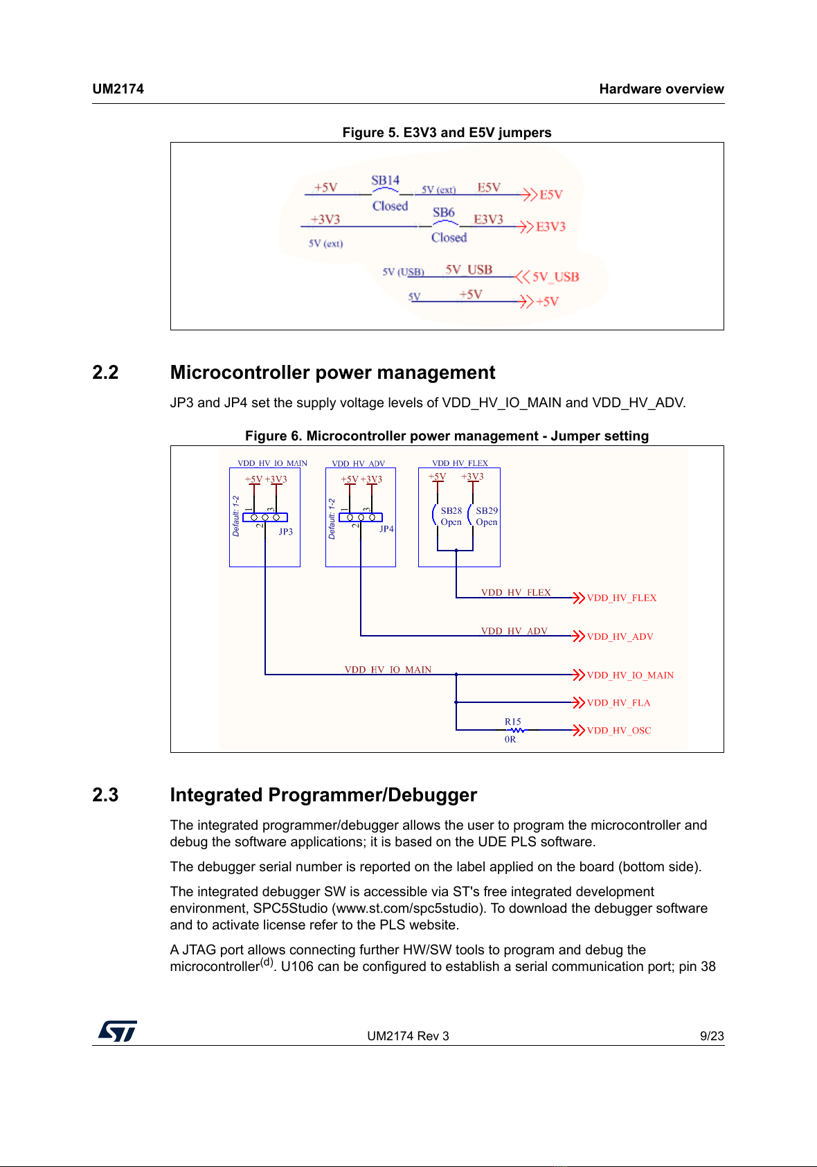
21
2 Hardware overview
2.1 Power supply section
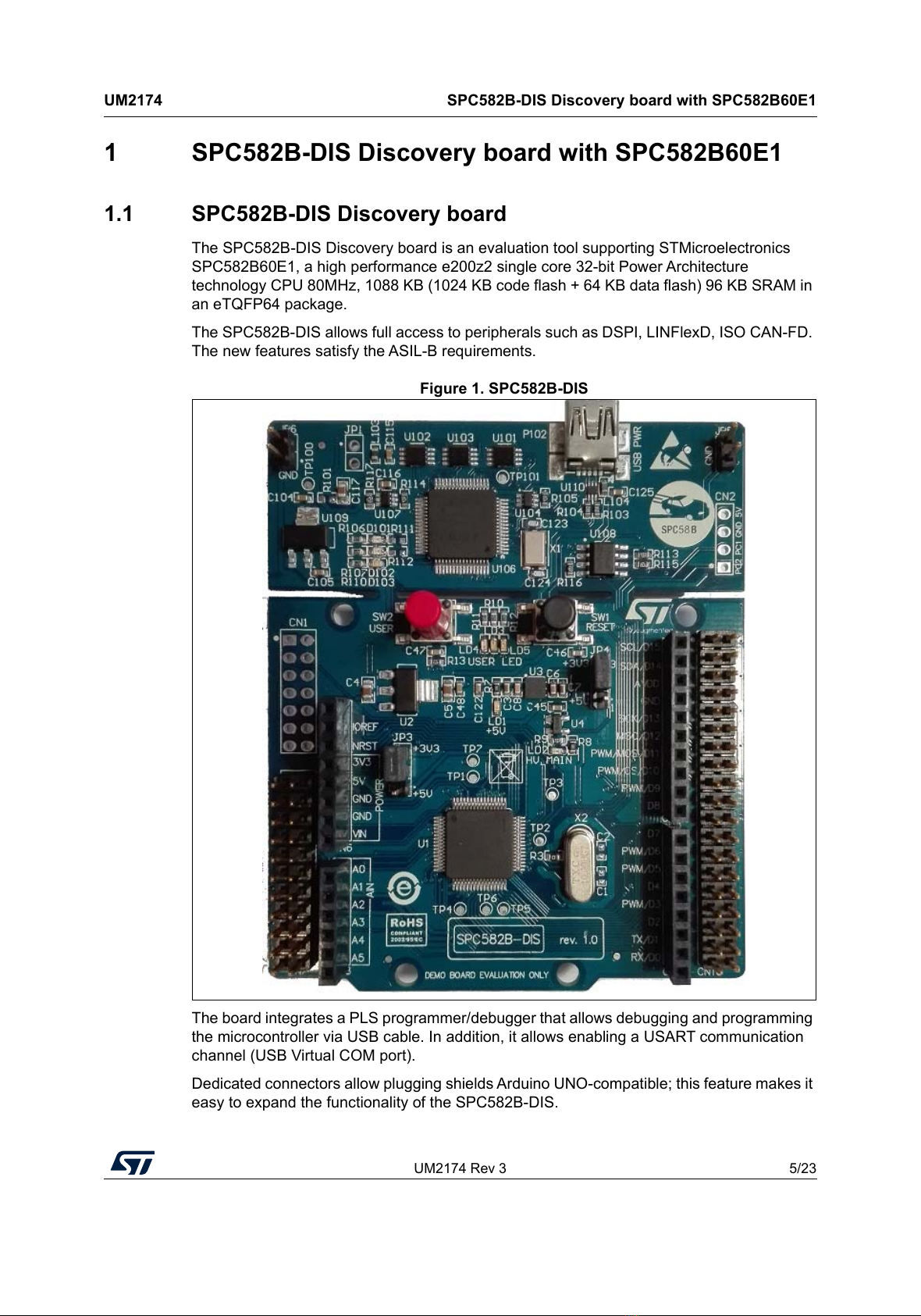
SPC582B-DIS can be supplied by using some DC sources, setting some jumpers properly:
by the host PC through the USB cable (+5 V; this is the default configuration);
by an external source connected to VIN pin (CN6 pin 8, CN7 pin 8) (7÷12V(b))
by an external source connected to E5V (CN6 pin 5, CN7 pin 17 and CN10 pin 8)
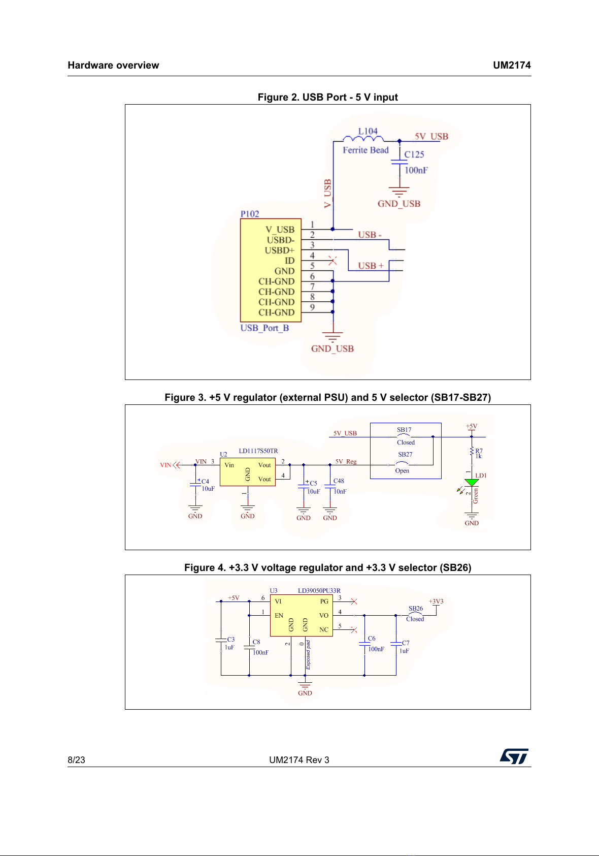
by an external source connected both to E3V3 (CN6 pin4 and CN7 pin 15) and to E5V
The external source can be a PSU, or the user application. The external sources or the
PSUs connected to the board must be SELV(c) compliant, self-protected and with limited
current capability.
2.1.1 Jumpers configuration cable
2.1.2 Voltage regulators and jumpers
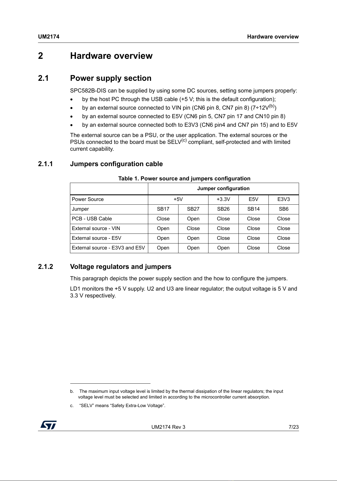
This paragraph depicts the power supply section and the how to configure the jumpers.
LD1 monitors the +5 V supply. U2 and U3 are linear regulator; the output voltage is 5 V and
3.3 V respectively.
b. The maximum input voltage level is limited by the thermal dissipation of the linear regulators; the input
voltage level must be selected and limited in according to the microcontroller current absorption.
c. “SELV” means “Safety Extra-Low Voltage”.
Table 1. Power source and jumpers configuration
Jumper configuration
Power Source +5V +3.3V E5V E3V3
Jumper SB17 SB27 SB26 SB14 SB6
PCB - USB Cable Close Open Close Close Close
External source - VIN Open Close Close Close Close
External source - E5V Open Open Close Close Close
External source - E3V3 and E5V Open Open Open Close Close