ST SPC58NHADPT176S User manual

Introduction
The SPC58NHADPT176S Rev.A evaluation board supports STMicroelectronics SPC58NH92 microcontroller in LQFP
24X24X1.4 176L.
Figure 1. SPC58NHADPT176S Rev.A
Note: picture not contractual
SPC58NHADPT176S Rev.A evaluation board
UM2731
User manual
UM2731 - Rev 1 - September 2020
For further information contact your local STMicroelectronics sales office.
www.st.com

1Overview
The SPC58NHADPT176S Rev. A mini module is an evaluation board supporting STMicroelectronics SPC58NH92
microcontroller in LQFP 24X24X1.4 176L package (LQFP 24X24X1.4 176L P0.5 EXPOSED PAD).
This mini module is designed to be connected onto the SPC58XXMB/SPC57XXMB motherboard, offering a
mechanism for easy customer evaluation of the supported devices, and to facilitate hardware and software
development.
The mini module may be used as a stand-alone unit allowing access to the CPU, but not to access to the I/O pins
nor any motherboard peripherals.
1.1 Package contents
A SPC58NHADPT176S Rev. A adapter package includes the following items:
• SPC58NHADPT176S Rev. A mini module
1.2 Supported devices
The SPC58NHADPT176S Rev. A mini module supports the SPC58NH family in LQFP 24X24X1.4 176L package.
UM2731
Overview
UM2731 - Rev 1 page 2/37

2License agreement
The packaging of this evaluation board was sealed with a seal stating, “by breaking this seal, you agree to the
terms and conditions of the evaluation board license agreement, the terms and conditions of which are available
at http://www.st.com/ebla”. Upon breaking the seal, you and STMicroelectronics entered into the evaluation board
license agreement, a copy of which is also enclosed with the evaluation board for convenience.
Attention: This evaluation board only offers limited features for evaluating ST products. It has not been tested for use with
other products and is not suitable for any safety or other commercial or consumer application. This evaluation
board is otherwise provided “AS IS” and STMicroelectronics disclaims all warranties, express or implied,
including the implied warranties of merchantability and fitness for a particular purpose.
UM2731
License agreement
UM2731 - Rev 1 page 3/37

3Handling precautions
Please take care to handle the package contents in a manner such as to prevent electrostatic discharge.
Before the EVB is used or power is applied, please fully read the following sections on how to correctly configure
the board. Failure to correctly configure the board may cause irreparable component, MCU or EVB damage.
UM2731
Handling precautions
UM2731 - Rev 1 page 4/37

4Hardware description
4.1 Hardware features
The SPC58NHADPT176S Rev. A mini module board has the following features:
• Connector for external power supplies input (5V) used in stand-alone mode
• Reset button with driver and led indicator
• Socket for device in LQFP 24X24X1.4 176L package
• Debug interfaces:
– 14-pin header connector for JTAG interface
– 10-pin header connector for JTAG/LFAST LVDS interface
– 10-pin header connector for SIPI interface
• 40 MHz crystal main oscillator with jumpers to optionally disconnect it
• 8 MHz oscillator with jumpers to optionally disconnect it
• Clock input through SMA connector with jumper to optionally disconnect it
• 2 X SAMTEC QSH series, 240-way connector to connect mini module to Motherboard
• 1 Gb/s Ethernet port
• HyperRAM and HyperFlash connected to HyperBUS interface
• Embedded eMMC device
• SD/MMC Card Reader
• 12x2 I/O connector
UM2731
Hardware description
UM2731 - Rev 1 page 5/37

4.2 Hardware dimension
The mini module has the following dimensions:
• PCB area: 127 mm x 114.3 mm
• Top components height: 19 mm max
• Bottom components height: 3.5 mm max
• PCB thickness: 1.6 mm
Figure 2. SPC58NHADPT176S Rev. A top component view
UM2731
Hardware dimension
UM2731 - Rev 1 page 6/37

5Power and system configuration
5.1 Power supplies
The mini module can be powered by providing voltages either supplied externally by the 2-Way PCB screw
connector (CN1) or supplied by the motherboard.
When the mini module is connected to the motherboard (MB), 3V3 and 5V0 are supplied by MB connector
selecting the associated jumpers. In this setup the external power supply input available on the mini module
MUST NOT BE USED.
When the SPC58NHADPT176S Rev. A mini module is used as a stand-alone board, 5V0 voltages must be
supplied externally, 3V3 and 1V2 voltages will be generated internally by specific circuit on the mini module.
The following jumpers are used to configure the power supply (common for all supported devices):
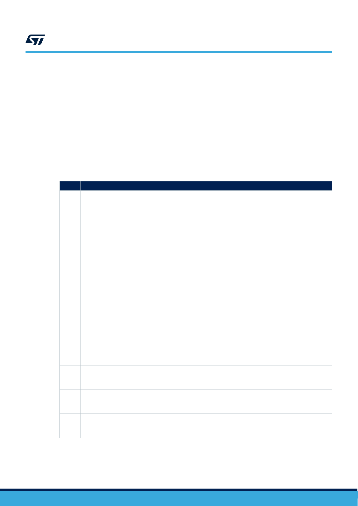
Table 1. Power configuration jumpers
Jumper Description Default Position
J1
5.0V source for J3 pin1 (MB_5.0V_LR or 5.0
V_ADC) voltage configuration:
• 1-2 MB_5.0V_LR
• 2-3 5.0 V_ADC
2-3
(5.0V_ADC)
Figure 8. Overview of
SPC58NHADPT176S Rev. A mini
module - Top - C3
J2
5.0V switching voltage configuration:
• 1-2 5 V EXT (external 5.0V supply)
• 2-3 MB_5.0V_SR (5.0V from
Motherboard)
2-3
(MB_5.0V_SR)
Figure 8. Overview of
SPC58NHADPT176S Rev. A mini
module - Top - D4
J3
VDD_HV_ADR_S / VDD_HV_ADV voltage
configuration:
• 1-2 5.0V source from J1 pin2
• 2-3 3.3 V_ADC source from J4 pin2
1-2
(5.0V_ADV)
Figure 8. Overview of
SPC58NHADPT176S Rev. A mini
module - Top - C3
J4
3V3 source (3.3V or MB_3.3V_SR) voltage
configuration:
• 1-2 3.3V (3.3V from mini module)
• 2-3 MB_3.3V_SR
1-2
(3.3V)
Figure 8. Overview of
SPC58NHADPT176S Rev. A mini
module - Top - D3
J5
Main MCU supply (VDD_HV_IO_MAIN) voltage
configuration:
• 1-2 5.0V_SR
• 2-3 3.3 V_SR from J4 pin2
1-2
(5.0V_SR)
Figure 8. Overview of
SPC58NHADPT176S Rev. A mini
module - Top - D3
J6
Supply for BALLAST circuit configuration
• 1-2 VDD_HV_IO_MAIN
• 2-3 5.0V_SR
1-2
(VDD_HV_IO_MAIN)
Figure 8. Overview of
SPC58NHADPT176S Rev. A mini
module - Top - D3
J7
BALLAST CIRCUIT ENABLE
• Closed: enable
• Open: disable
Closed
(enable)
Figure 8. Overview of
SPC58NHADPT176S Rev. A mini
module - Top - D2
J8
VDD_LV voltage configuration:
• 1-2 (1.2V_SR from J9 pin2)
• 2-3 (BALLAST circuit)
1-2
(1.2V_SR)
Figure 8. Overview of
SPC58NHADPT176S Rev. A mini
module - Top - C3
J9
1.2V_SR switching configuration:
• 1-2 MB_1.25V_SR (1.25V from MB)
• 2-3 1.2V (1.2V from mini module)
2-3
(1.2V from mini module)
Figure 8. Overview of
SPC58NHADPT176S Rev. A mini
module - Top - D3
UM2731
Power and system configuration
UM2731 - Rev 1 page 7/37

5.2 JTAG/LFAST LVDS interface configuration
The following jumpers need to configure the JTAG/LFAST LVDS/SIPI:
Table 2. JTAG/LFAST/SIPI Configuration jumpers
Jumper Description Default Position
J10
SIPI pin 3 configuration
• 1-2: RDY
• 2-3: PA14
1-2
(RDY) Figure 8. Overview of SPC58NHADPT176S Rev. A mini module - Top - A4
J11
TDI_LF configuration
• 1-2: TDI_LF
• 2-3: PA8
1-2
(TDI_LF) Figure 8. Overview of SPC58NHADPT176S Rev. A mini module - Top - A4
J12
TDO_LF configuration
• 1-2: TDO_LF
• 2-3: PA9
1-2
(TDO_LF) Figure 8. Overview of SPC58NHADPT176S Rev. A mini module - Top - A4
J13
JTAG pin 13 configuration
• 1-2: EVTO
• 2-3: PJ3/PQ4
1-2
(EVTO) Figure 8. Overview of SPC58NHADPT176S Rev. A mini module - Top - B4
J14
PC1 / ESR0
• 1-2 ESR0
• 2-3 PC1
1-2
(ESR0) Figure 8. Overview of SPC58NHADPT176S Rev. A mini module - Top - B4
J15
EVTO/ESR0
• 1-2 ESR0
• 2-3 EVTO
1-2
(ESR0) Figure 8. Overview of SPC58NHADPT176S Rev. A mini module - Top - B4
UM2731
JTAG/LFAST LVDS interface configuration
UM2731 - Rev 1 page 8/37

5.3 System clock configuration
The mini module supports the usage of crystal clock sources as well as external clock source:
Table 3. Clock configuration jumpers
Jumper Description Default Position
J20
XTAL32 configuration
• Close: connect pin 2 of 32.768 KHz crystal
(Y2) to XTAL32
Open Figure 8. Overview of SPC58NHADPT176S
Rev. A mini module - Top - C3
J21
EXTAL32 configuration
• Close: connect pin 1 of 32.768 KHz crystal
(Y2) to EXTAL32
Open Figure 8. Overview of SPC58NHADPT176S
Rev. A mini module - Top - C3
J17
EXTAL configuration
• 1-2 connect pin 2 of 40 MHz crystal (Y1) to
EXTAL
• 2-3 connect EVB-EXTAL to EXTAL
1-2
(Y1 pin2 to
EXTAL)
Figure 8. Overview of SPC58NHADPT176S
Rev. A mini module - Top - C2
J19
XTAL configuration
• 1-2 connect pin 1 of 40 MHz crystal (Y1) to
XTAL
• 2-3 connect XTAL to GND
1-2
(Y1 pin1 to
XTAL)
Figure 8. Overview of SPC58NHADPT176S
Rev. A mini module - Top - C2
J18
Enable 8 MHz oscillator power supply
• open - power off
• closed - power on
Open
(power off)
Figure 8. Overview of SPC58NHADPT176S
Rev. A mini module - Top - C1
J22
External 8 MHz clock source
• 1-2 OSC-MOD (from oscillator)
• 2-3 EXTAL-SMA (from SMA connector)
1-2
(8 MHz from
oscillator)
Figure 8. Overview of SPC58NHADPT176S
Rev. A mini module - Top - C2
5.4 Reset circuit
The mini module supports different ways to reset the microcontroller. To use and perform the reset driving there
are different jumpers and switches:
Table 4. Reset configuration jumpers
Jumper Description Default Position
SW1 Reset push button Open Figure 8. Overview of SPC58NHADPT176S Rev. A
mini module - Top - A4
J24
Connect the external
reset to the reset driver
for ESR0 and PORST
pins
Close Figure 8. Overview of SPC58NHADPT176S Rev. A
mini module - Top - C4
J23 Connect the external
reset to ESR0 pin Close Figure 8. Overview of SPC58NHADPT176S Rev. A
mini module - Top - C4
J25 Connect the external
reset to PORST pin Close Figure 8. Overview of SPC58NHADPT176S Rev. A
mini module - Top - C4
UM2731
System clock configuration
UM2731 - Rev 1 page 9/37

5.5 Other Jumpers
Table 5. Other jumpers
Jumper Description Default Position
J16 TESTMODE settings Close
(10 KΩ down)
Figure 8. Overview of SPC58NHADPT176S Rev. A
mini module - Top - B2
5.6 Configuration for pin shared between HyperBus & eMMC
The jumpers described into the following table allow you to configure the pins shared between HyperBus and
eMMC.
Table 6. Pin shared between HyperBus & eMMC jumper
Jumper Description Default configuration Position
J27
Data4 - PF9 configuration
• 1-2 DQ4_HB
(HyperBus)
• 2-3 D4_eMM
(eMMC)
1-2
(HyperBus)
Figure 8. Overview of SPC58NHADPT176S Rev. A
mini module - Top - B2
J29
Data5 – PF10
configuration
• 1-2 DQ5_HB
(HyperBus)
• 2-3 D5_eMM
(eMMC)
1-2
(HyperBus)
Figure 8. Overview of SPC58NHADPT176S Rev. A
mini module - Top - B2
J31
Data6 - PF11
configuration
• 1-2 DQ6_HB
(HyperBus)
• 2-3 D6_eMM
(eMMC)
1-2
(HyperBus)
Figure 8. Overview of SPC58NHADPT176S Rev. A
mini module - Top - B2
J34
Data7 - PF12
configuration
• 1-2 DQ7_HB
(HyperBus)
• 2-3 D7_eMM
(eMMC)
1-2
(HyperBus)
Figure 8. Overview of SPC58NHADPT176S Rev. A
mini module - Top - B2
UM2731
Other Jumpers
UM2731 - Rev 1 page 10/37

5.7 Configuration for pin shared between eMMC & SD-card reader
The jumpers described into the following table allow you to configure the pins shared between SD-CARD
READER and eMMC.
Table 7. Pin shared between eMMC & SD-card reader jumper
Jumper Description Default configuration Position
J30
Data1 - PJ4 configuration
• 1-2 D1_SD (SD-
CARD)
• 2-3 D1_eMM
(eMMC)
1-2
(SD-CARD)
Figure 8. Overview of SPC58NHADPT176S Rev. A
mini module - Top - C1/C2
J32
Data2 - PH5 configuration
• 1-2 D2_SD (SD-
CARD)
• 2-3 D2_eMM
(eMMC)
1-2
(SD-CARD)
Figure 8. Overview of SPC58NHADPT176S Rev. A
mini module - Top - C1/C2
J35
Data3 - PH6 configuration
• 1-2 D3_SD (SD-
CARD)
• 2-3 D3_eMM
(eMMC)
1-2
(SD-CARD)
Figure 8. Overview of SPC58NHADPT176S Rev. A
mini module - Top - C1/C2
J28
CLK - PJ2 configuration
• 1-2 CLK_SD (SD-
CARD)
• 2-3 CLK_eMM
(eMMC)
1-2
(SD-CARD)
Figure 8. Overview of SPC58NHADPT176S Rev. A
mini module - Top - C1/C2
J33
FBCLK - PJ0
configuration
• 1-2 FBCLK_SD
(SD-CARD)
• 2-3 FBCLK_eMM
(eMMC)
1-2
(SD-CARD)
Figure 8. Overview of SPC58NHADPT176S Rev. A
mini module - Top - C2/C3
J36
CMD - PJ1 configuration
• 1-2 CMD_SD (SD-
CARD)
• 2-3 CMD_eMM
(eMMC)
1-2
(SD-CARD)
Figure 8. Overview of SPC58NHADPT176S Rev. A
mini module - Top - C2
UM2731
Configuration for pin shared between eMMC & SD-card reader
UM2731 - Rev 1 page 11/37

6Hardware description
6.1 1 Gb/s ethernet interface
This paragraph describes the 1 Gb/s Ethernet interface present on the mini module.
The Ethernet connector is RJ-45 with integrated magnetics.
The following figure shows the functional diagram of the Ethernet interface.
Figure 3. 1 Gb/s Ethernet functional diagram
The figure below shows the Ethernet ESD protection schema.
Figure 4. 1 Gb/s Ethernet ESD protection schema
U9
HSP061-4M10Y
I/0 1
1
I/0 2
2
GND
3
I/0 3
4
I/0 4
5NC1 6
NC2 7
GND 8
NC3 9
NC4 10
TXRXM_B
TXRXP_B
GND GND
TXRXM_A
TXRXP_A TXRXP_A
TXRXP_B
TXRXM_B
TXRXM_A
U10
HSP061-4M10Y
I/0 1
1
I/0 2
2
GND
3
I/0 3
4
I/0 4
5NC1 6
NC2 7
GND 8
NC3 9
NC4 10
GND GND
TXRXM_D
TXRXP_D
TXRXM_C
TXRXP_C
TXRXM_D
TXRXP_C
TXRXM_C
TXRXP_D
The following table describes all hardware of 1 Gb/s Ethernet interface of the mini module, their position on PCB.
Table 8. 1 Gb/s Ethernet interface
Jumper Description Position
U9 ESD Protection Figure 8. Overview of SPC58NHADPT176S Rev. A mini module - Top - A3
U10 ESD Protection Figure 8. Overview of SPC58NHADPT176S Rev. A mini module - Top - A3
U11 Ethernet 1-Port GigabitEthrnt
Ethernet PHY Figure 8. Overview of SPC58NHADPT176S Rev. A mini module - Top - A2/A3
U19 Ethernet connector Figure 8. Overview of SPC58NHADPT176S Rev. A mini module - Top - A3/B3
UM2731
Hardware description
UM2731 - Rev 1 page 12/37

6.2 Hyperbus interface
This paragraph describes the Hyperbus interface present on the mini module.
The SPC58NHADPT176S contains only one CS (CNS), whereas the memory device contains two CSs lines, one
for RAM and one for FLASH.
The second CS is emulated using one GPIO signal (PA[15]).
The following table shows the logic between CS/GPIO from SPC58NHADPT176S and CS0/CS1 from HyperRAM/
HyperFlash device.
Table 9. Hyperbus CS truth table
CSN GPIO CS0 CS1
0 0 1 0
0 1 0 1
1 0 1 1
1 1 0 1
The logic can be realized using the scheme of the figure below.
Figure 5. Hyperbus CS scheme
The following table describes all hardware HyperBus of the mini module, their position on PCB.
Table 10. Hyperbus interface
Symbol Description Position
U14 CMOS inverter Figure 9. Overview of SPC58NHADPT176S Rev. A mini module - Bottom - C1
IC1 TTL OR gate Figure 8. Overview of SPC58NHADPT176S Rev. A mini module - Top - B1
U13 RAM 256 Mbit Figure 8. Overview of SPC58NHADPT176S Rev. A mini module - Top - B2
UM2731
Hyperbus interface
UM2731 - Rev 1 page 13/37

6.3 eMMC interface
This paragraph describes the embedded eMMC device present on the mini module.
The figure below shows the functional diagram of the eMMC interface.
Figure 6. eMMC functional diagram
The following table describes all hardware the eMMC interface of the mini module and their position on PCB.
Table 11. eMMC interface
Symbol Description Position
U15 eMMC Memory 8 GB Figure 8. Overview of SPC58NHADPT176S Rev. A mini module - Top - B1
UM2731
eMMC interface
UM2731 - Rev 1 page 14/37

6.4 SD/MMC interface
This paragraph describes the card reader JEDED/MMC standard version 5.0 compliant.
The filter used is EMIF06-MSD02N16 by ST.
The SD/MMC card reader needs to use a power switch to limit the output current to a safe level in case the output
load exceeds the current limits threshold or a short is present.
Use a STMPS2151MTR by ST.
The figure below shows SD/MMC card reader diagram.
Figure 7. SD/MMC card reader diagram
The following table describes all hardware of the SD/MMC interface of the mini module and their position on PCB.
Table 12. SD/MMC interface
Symbol Description Position
U16 CMOS switch Figure 9. Overview of SPC58NHADPT176S Rev. A mini module - Bottom - A2
U17 Filter EMI 6-line Micro Figure 9. Overview of SPC58NHADPT176S Rev. A mini module - Bottom - B2
U18 Connector SD reverse push-push Figure 8. Overview of SPC58NHADPT176S Rev. A mini module - Top - D1/D2
UM2731
SD/MMC interface
UM2731 - Rev 1 page 15/37

6.5 Test points
The mini module has several test points, described in the table below.
Table 13. Test points
Test point Description Position
TP0 VDD_HV_IO_MAIN Figure 8. Overview of SPC58NHADPT176S Rev. A mini module - Top - D3
TP1 VSS_OSC Figure 8. Overview of SPC58NHADPT176S Rev. A mini module - Top - C2
TP2 AGND Figure 8. Overview of SPC58NHADPT176S Rev. A mini module - Top - C3
TP3 JCOMP_RxDATA_N/PA[5] Figure 8. Overview of SPC58NHADPT176S Rev. A mini module - Top - A2
TP4 TCK/PA[6] Figure 8. Overview of SPC58NHADPT176S Rev. A mini module - Top - A1
TP5 TMS_TxDATA_P/PA[7] Figure 8. Overview of SPC58NHADPT176S Rev. A mini module - Top - A2
TP6 TXD0 Figure 8. Overview of SPC58NHADPT176S Rev. A mini module - Top - B3
TP7 TXD1 Figure 8. Overview of SPC58NHADPT176S Rev. A mini module - Top - B3
TP8 TXD2 Figure 8. Overview of SPC58NHADPT176S Rev. A mini module - Top - B2
TP9 TXD3 Figure 8. Overview of SPC58NHADPT176S Rev. A mini module - Top - B2
TP10 GTX_CLK Figure 8. Overview of SPC58NHADPT176S Rev. A mini module - Top - B2
TP11 INT_N (on U11) Figure 8. Overview of SPC58NHADPT176S Rev. A mini module - Top - A2
TP12 MDC Figure 8. Overview of SPC58NHADPT176S Rev. A mini module - Top - B2
TP13 MDIO Figure 8. Overview of SPC58NHADPT176S Rev. A mini module - Top - B2
TP14 CK_HB Figure 8. Overview of SPC58NHADPT176S Rev. A mini module - Top - B2
TP15 D0_HB Figure 8. Overview of SPC58NHADPT176S Rev. A mini module - Top - C2
TP16 D1_HB Figure 8. Overview of SPC58NHADPT176S Rev. A mini module - Top - B2
TP17 D2_HB Figure 8. Overview of SPC58NHADPT176S Rev. A mini module - Top - B2
TP18 D3_HB Figure 8. Overview of SPC58NHADPT176S Rev. A mini module - Top - B2
TP19 D4_HB Figure 8. Overview of SPC58NHADPT176S Rev. A mini module - Top - B2
TP20 D5_HB Figure 8. Overview of SPC58NHADPT176S Rev. A mini module - Top - B2
TP21 D6_HB Figure 8. Overview of SPC58NHADPT176S Rev. A mini module - Top - B2
TP22 D7_HB Figure 8. Overview of SPC58NHADPT176S Rev. A mini module - Top - B2
TP23 RWDS_HB Figure 8. Overview of SPC58NHADPT176S Rev. A mini module - Top - B2
TP24 CMD_eMM Figure 8. Overview of SPC58NHADPT176S Rev. A mini module - Top - B2
TP25 FAULT (on U16) Figure 8. Overview of SPC58NHADPT176S Rev. A mini module - Top - C2
TP26 RDAT3_GND (on U17) Figure 8. Overview of SPC58NHADPT176S Rev. A mini module - Top - C2
TP27 1.2V_ETH Figure 8. Overview of SPC58NHADPT176S Rev. A mini module - Top - A2
TP28 GND Figure 8. Overview of SPC58NHADPT176S Rev. A mini module - Top - A4
TP29 GND Figure 8. Overview of SPC58NHADPT176S Rev. A mini module - Top - A1
TP30 GND Figure 8. Overview of SPC58NHADPT176S Rev. A mini module - Top - D1
TP31 GND Figure 8. Overview of SPC58NHADPT176S Rev. A mini module - Top - D4
UM2731
Test points
UM2731 - Rev 1 page 16/37

6.6 Connectors
The mini module has other connectors described in the table below:
Table 14. Other connectors
Connectors Description
CN3 14-pin header connector for JTAG interface
CN4 10-pin header connector for JTAG/LFAST LVDS interface
CN2 10-pin header connector for SIPI interface
CN5, CN6 2 X SAMTEC QSH series, 240-way connector to connect mini module to Motherboard
CN1 External power supplies input (5V)
P1 SMA connector for external clock input
U18 SD revers connector
FCCU1 FCCU TEST CONNECTOR
UM2731
Connectors
UM2731 - Rev 1 page 17/37

7Layout overview
Figure 8. Overview of SPC58NHADPT176S Rev. A mini module - Top
PCB CODE: SCI20180510
A B C D
1
2
3
4
UM2731
Layout overview
UM2731 - Rev 1 page 18/37

Figure 9. Overview of SPC58NHADPT176S Rev. A mini module - Bottom
A B C D
1
2
3
4
UM2731
Layout overview
UM2731 - Rev 1 page 19/37

8BOM
Table 15. BOM
Itm Qty Ref.
designator Value Description Manufacturer Manufcode
1 39
CF1, C11,
C12, C16,C19,
C22, C25,
C28, C42,
C47, C50,
C53, C56,
C79, C85,
C86, C87,
C89, C90,
C92, C95,
C96, C97,
C99, C103,
C104,
C105 ,C106,
C107, C108,
C110, C111,
C112, C113,
C114, C115,
C116, C117,
C118
100 nF Mult. cer. cap. Murata GCM188R71H104KA57D
2 1 CN1 2V1P Screw terminal block,
1 row (N4)
3 1 CN2 ERF8-005-05.0-L-DV-L-
TR
Conn rugged female
10 pin, high speed Samtec ERF8-005-05.0-L-DV-L-
TR
4 1 CN3 N2514-6002RB Conn flat male 14 pin,
180° 3M N2514-6002RB
5 1 CN4 Samtec TFM-105-02-L-
D-WT
Conn TFM 10 pin,
with weld tabs Samtec TFM-105-02-L-D-WT
6 2 CN5, CN6 SAMTEC QSH-120-01-
L-D-A
Female conn 240 pin,
2 row Samtec QSH-120-01-L-D-A
7 4 C1, C2, C3, C4 4.7 uF Mult. cer. cap. Murata GRM32ER71H475KA88L
8 8
C5, C6, C9,
C10, C74,
C75, C76, C77
DNM Mult. cer. cap. - not
mounted
9 7
C7, C8, C15,
C30, C33,
C36, C39
2.2 uF Mult. cer. cap. Murata GCM21BR71C225KA64L
10 19
C13, C14,
C17, C20,
C23, C26,
C29, C32,
C35, C38,
C41, C43,
C45, C48,
C51,
C54 ,C57,
C93, C100
10 nF Mult. cer. cap. Murata GCM188R71H103KA37D
11 8
C18, C21,
C24, C27,
C46, C49,
C52, C55
4.7 uF Mult. cer. cap. Murata GCM21BR71C475KA73
UM2731
BOM
UM2731 - Rev 1 page 20/37
Table of contents
Other ST Motherboard manuals

ST
ST STM32303C-EVAL User manual

ST
ST L9679E-EVB User manual

ST
ST STM32H7B3I-EVAL User manual

ST
ST EVAL-TDA7803A User manual

ST
ST ST9 EPB User manual

ST
ST User Manual User manual

ST
ST SPC58XXADPT144S REV.B User manual

ST
ST STM32F746G-DISCO User manual

ST
ST STEVAL-ILH007V1 User manual

ST
ST SPC58NG-DISP User manual

ST
ST STM32F407 Series User manual

ST
ST STM32 Nucleo-64 User manual

ST
ST SPC58XXADPT292S User manual

ST
ST STM32G4 Nucleo-64 User manual

ST
ST AEK-MOT-TK200G1 User manual

ST
ST EVAL-IBD002-35W User manual

ST
ST STEVAL-ISF003V1 User manual

ST
ST NUCLEO-F207ZG User manual

ST
ST SPC574KADPT144S User manual

ST
ST NUCLEO-F207ZG User manual