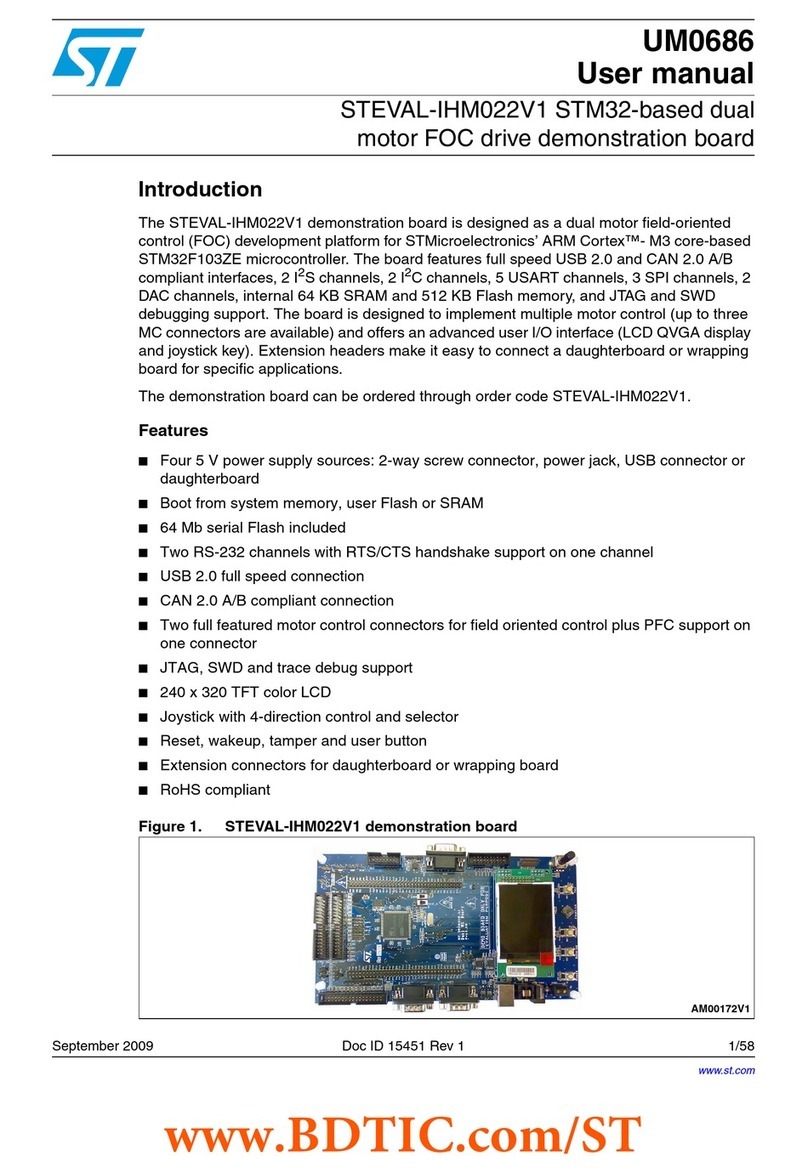
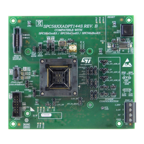
ST STM32H757I-EVAL User manual

Introduction
The STM32H747I-EVAL and STM32H757I-EVAL Evaluation boards (STM32H7x7I-EVAL) are high-end development platforms
for the Arm® Cortex®-M7-based STM32H747XI and STM32H757XI microcontrollers (STM32H7x7XI), respectively. The
STM32H7x7I-EVAL Evaluation boards provide access to all the STM32 peripherals for user applications, and include an
embedded STLINK-V3E debugger/programmer.
The full range of the STM32H7x7I-EVAL hardware features helps develop applications and evaluate all peripherals: USB
OTG_HS and FS, Ethernet, FDCAN, USART, Audio DAC and ADC, digital microphone, SRAM, SDRAM, NOR Flash memory,
Twin Quad-SPI Flash memory, microSD™ 3.0 card, 4” 480×800 TFT color LCD with MIPI DSISM interface and capacitive
touchpanel, and cryptographic hardware accelerator (available only on STM32H757XI devices) .
The expansion connectors provide an easy way to add specialized features, while ETM trace is supported through external
probes.
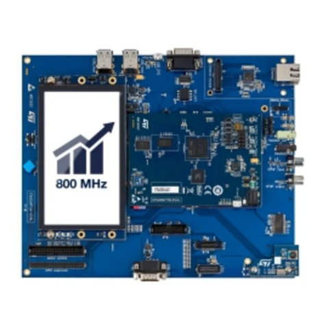
Figure 1. STM32H7x7I-EVAL board (top view)
Picture is not contractual.
Evaluation boards with STM32H747XI and STM32H757XI MCUs
UM2525
User manual
UM2525 - Rev 3 - May 2019
For further information contact your local STMicroelectronics sales office. www.st.com

1Features
• STM32H747XIH6 and STM32H757XIH6 microcontrollers with 2 Mbytes of Flash memory and 1 Mbyte of
RAM in TFBGA240+25 package
• 4” 480×800 TFT color LCD with MIPI DSISM interface and capacitive touchpanel
• Ethernet compliant with IEEE-802.3-2002
• USB OTG_HS and OTG_FS
• I2C compatible serial interface
• RTC with rechargeable backup battery
• SAI audio DAC
• ST-MEMS digital microphones
• 8-Gbyte (or more) SDIO3.0 interface microSD™ card
• 8 M×32bit SDRAM, 1 M×16bit SRAM and 8 M×16bit NOR Flash memory
• 1-Gbit Twin Quad-SPI NOR Flash memory or two 512-Mbit Quad-SPI NOR Flash memories
• Potentiometer
• 4 color user LEDs
• Reset, wakeup, tamper or key buttons
• Joystick with 4-direction control and selector
• Board connectors
– Power jack
– 3 USB interfaces with Micro-AB connector
– RS-232 communications
– Ethernet RJ45
– FDCAN compliant connection
– Stereo headset jack including analog microphone input
– 2 audio jacks for external speakers
– microSD™ card
– JTAG/SWD and ETM trace
– Extension connectors and memory connectors for daughterboard or wire-wrap board
• Flexible power-supply options: ST-LINK USB VBUS or external sources
• On-board STLINK-V3E debugger/programmer with USB re-enumeration capability: mass storage, Virtual
COM port, and debug port
• Comprehensive free software libraries and examples available with the STM32Cube MCU Package
• Support of a wide choice of Integrated Development Environments (IDEs) including IAR™, Keil®, GCC-
based IDEs
Note: Arm is a registered trademark of Arm Limited (or its subsidiaries) in the US and/or elsewhere.
UM2525
Features
UM2525 - Rev 3 page 2/69

2Ordering information
To order STM32H747I-EVAL and STM32H757I-EVAL refer to Table 1. Ordering information. Additional information
is available from the datasheet and reference manual of the target STM32.
Table 1. Ordering information
Order code Board reference Target STM32 Differentiating features
STM32H747I-EVAL • MB1246
• MB1166(1)
STM32H747XIH6U -
STM32H757I-EVAL STM32H757XIH6U Cryptography
1. LCD board.
2.1 Product marking
Evaluation tools marked as “ES” or “E” are not yet qualified and therefore not ready to be used as reference
design or in production. Any consequences deriving from such usage will not be at ST charge. In no event, ST will
be liable for any customer usage of these engineering sample tools as reference design or in production.
“E” or “ES” marking examples of location:
• On the targeted STM32 that is soldered on the board (for illustration of STM32 marking, refer to the STM32
datasheet “Package information” paragraph at the www.st.com website).
• Next to the evaluation tool ordering part number that is stuck or silk-screen printed on the board.
Some boards feature a specific STM32 device version, which allows the operation of any bundled commercial
stack/library available. This STM32 device shows a "U" marking option at the end of the standard part number
and is not available for sales.
In order to use the same commercial stack in his application, a developer may need to purchase a part number
specific to this stack/library. The price of those part numbers includes the stack/library royalties.
2.2 Codification
The meaning of the codification is explained in Table 2. The order code is mentioned on a sticker placed on the
top side of the board.
Table 2. Codification explanation
STM32H7X7I-EVAL Description Example: STM32H757I-EVAL
H7 MCU series in STM32 Arm Cortex MCUs STM32H7 Series
X7 MCU product line in the series STM32H757
ISTM32 Flash memory size:
• I for 2 Mbytes 2 Mbytes
UM2525
Ordering information
UM2525 - Rev 3 page 3/69

3Development environment
3.1 System requirements
• Windows® OS (7, 8 and 10), Linux® 64-bit, or macOS®
• USB Type-A to Micro-B cable
Note: macOS® is a trademark of Apple Inc. registered in the U.S. and other countries.
3.2 Development toolchains
• Keil® MDK-ARM (see note)
• IAR™ EWARM (see note)
• GCC-based IDEs
Note: On Windows® only.
3.3 Demonstration software
The demonstration software, included in the STM32Cube MCU Package corresponding to the on-board
microcontroller, is preloaded in the STM32 Flash memory for easy demonstration of the device peripherals in
standalone mode. The latest versions of the demonstration source code and associated documentation can be
downloaded from www.st.com.
UM2525
Development environment
UM2525 - Rev 3 page 4/69

4Conventions
Table 3 provides the conventions used for the ON and OFF settings in the present document.
Table 3. ON/OFF convention
Convention Definition
Jumper JPx ON Jumper fitted
Jumper JPx OFF Jumper not fitted
Jumper JPx [1-2] Jumper should be fitted between Pin 1 and Pin 2
Solder bridge SBx ON SBx connections closed by 0 Ω resistor
Solder bridge SBx OFF SBx connections left open
Resistor Rx ON Resistor soldered
Resistor Rx OFF Resistor not soldered
UM2525
Conventions
UM2525 - Rev 3 page 5/69

5Delivery recommendations
Some verifications are needed before using the Evaluation board for the first time, to make sure that no damage
occurred during shipment and that no components are unplugged or lost.
When the board is extracted from its plastic bag, check that no component remains in the bag. The main
component to verify is the microSD card that may have been ejected from the connector CN13 (right side of the
board).
Caution: There is an explosion risk if the battery is replaced by an incorrect one. Make sure to dispose of used batteries
according to the instructions.
UM2525
Delivery recommendations
UM2525 - Rev 3 page 6/69

6STM32H7x7I-EVAL hardware layout and configuration
The STM32H7x7I-EVAL Evaluation boards are designed around the STM32H7x7XIH6U (240+25-pin TFBGA
package) microcontroller. Figure 2 shows the hardware block diagram for STM32H7x7XIH6U and illustrates the
connection between the microcontroller and the peripherals (SDRAM, SRAM, NOR Flash, Twin Quad-SPI Flash,
color LCD, USB OTG connectors, USART, Ethernet, Audio, FDCAN, microSD 3.0 card and embedded ST-LINK).
Figure 3. STM32H7x7I-EVAL Evaluation board (top side) helps users to locate these features on the Evaluation
board. The mechanical dimensions of the board are showed in Figure 4. STM32H7x7I-EVAL Evaluation board
mechanical drawing .
Figure 2. Hardware block diagram
STM32H7x7XIH6U
3V Battery
RTC
PHY &
Ethernet
connector
JTAG & trace
connector DAP
1 RS232 DB9
connector
32 KHz
Crystal
VBAT
STLINK-V3E
I2C
USB connector
SW & trace
connector TPIU
RMII
I2C connector
4" DSI LCD
MFX
Joystick and
LED
microSD card
CAN connector
FDCAN
Key, Wakeup &
Tamper buttons GPIO
ADC
SDMMC 3.0 HS PHY & USB
connector
OTG1
NOR Flash
memory
SRAM
FMC
SDRAM
QSPI
1Gb/
2x512Mb
Twin QSPI
Flash
memory(ies)
OTG2
FS USB connector
UART1
MIPI DSI
DFSDM
PDM
3.3V Power
supply
1.8V Power
supply
2.9V SD3.0
Power supply
Potentiometer
SAI1
Audio DAC &
amplifier
UM2525
STM32H7x7I-EVAL hardware layout and configuration
UM2525 - Rev 3 page 7/69

6.1 STM32H7x7I-EVAL Evaluation board layout
Figure 3. STM32H7x7I-EVAL Evaluation board (top side)
CN4
I2C extension
connector
CN2
USART1
CN3
FDCAN
U27 (CN25)
Left Digital
Microphone
(Coupon
connectors)
B3
Tamper
Button
B4
Joystick
B2
Wakeup
Button
B1
Reset
Button
RV1
Potentiometer
4 colors
LEDs
LD12
ST-LINK/V3E
COM LED
CN23
ST-LINK/V3E
USB
CN18
USB OTG2
FS
CN16
USB OTG1 FS
CN14
USB OTG1
HS
CN10
Power jack
CN11,CN12
Memory header
U7
STM32H7xxI
CN6,CN7
Extension
header
CN1
Ethernet RJ45
Connector
CN8
ETM TRACE
CN24
STDC14
CN9
JTAG/SWD
CN15
LCD Connector
CN13
MicroSD card
CN20
LCD Connector
CN17
Headset
Audio jack
CN19
Speaker out
jack
LD11
STLINK-V3E
Power
overcurrent
Alarm
U26 (CN26)
Right Digital
Microphone
(Coupon
connectors)
UM2525
STM32H7x7I-EVAL Evaluation board layout
UM2525 - Rev 3 page 8/69

6.2 Ordering information
Figure 4 and Table 4 show the mechanical dimensions for the MB1246 board with the 5.7” LCD daughterboard.
Figure 4. STM32H7x7I-EVAL Evaluation board mechanical drawing
Table 4. Mechanical dimensions
Symbol Size(mm) Symbol Size(mm) Symbol Size(mm)
A1 68.58 H 8 P1 16.76
A2 48.62 Lx1 13.7 P2 55.32
a 1.27 Lx2 25 Q1 39.23
D 4.5 Ly1 5 Q2 9.98
d 3.5 Ly2 6.4 X 141.60
E 37.7 Mx 12.5 Y 172.72
e 116.5 My 32.7
UM2525
Ordering information
UM2525 - Rev 3 page 9/69

6.3 Embedded STLINK-V3E
The STLINK-V3E programming and debugging tool is integrated on the STM32H7x7I-EVAL Evaluation board.
The key STLINK-V3E features are the following:
• Standalone probe with modular extensions
• Self-powered through a USB connector (Micro-B)
• USB 2.0 high-speed compatible interface
• Direct firmware update support (DFU)
• JTAG/serial wire debugging (SWD) specific features:
– 3 to 3.6 V application voltage support and 5 V tolerant inputs
– Flat cables STDC14 to MIPI10 / STDC14 / MIPI20 (connectors with 1.27 mm pitch)
– JTAG communication support
– SWD and serial wire viewer (SWV) communication support
• Virtual COM port (VCP) specific features:
– 3 to 3.6 V application voltage support on the UART interface and 5 V tolerant inputs
– VCP frequency up to 15 MHz
– Available on STDC14 debug connector (not available on MIPI10)
• Multipath bridge USB to SPI/UART/I2C/CAN/GPIOs specific features:
– 3 to 3.6 V application voltage support and 5 V tolerant inputs
– Signals available on adapter board only (MB1440)
• Drag-and-drop Flash programming
• Two color LEDs: communication, power
Refer to http://www.st.com for details about STLINK-V3E.
Note: It is possible to power the Evaluation board through CN23 (Embedded STLINK/V3E USB connector) even if an
external tool is connected to CN8 (ETM Trace connector) or CN9 (External JTAG and SWD connector).
ETM can only work at 50 MHz clock by default because ETM signals are shared with other peripherals. If better
performance of ETM is required (84 MHz/98 MHz), R217, R230, R231, R234, R236, SB2, SB5, SB8, SB11,
SB42, SB57 must be removed to reduce the stub on ETM signals. In this configuration SAI and PDM are not
functional and NOR Flash and the address of SRAM are limited on A18.
ETM trace function would be abnormal as SAI_SDB share the same pins with TRACE_D0, and TRACE_D0
would be forced high by SAI_SDB. When using ETM trace it is necessary to set ADCDAT1 pin (SAI_SDB signal
of the STM32) of audio codec WM8994ECS/R (U22) by software to be tri-state.
6.3.1 Drivers and firmware upgrade
The STLINK-V3E requires drivers to be installed on Windows®. It embeds a firmware which needs to be updated
from time to time to benefit from new functionalities and bug corrections. Refer to technical note "Overview of ST-
LINK derivated" (TN1235) for details.
6.4 Power supply
The STM32H7x7I-EVAL Evaluation board is designed to be powered by 5 V DC power supply and is protected by
PolyZen from wrong power plug-in events. It is possible to configure the Evaluation board to use any of the
following six sources for the power supply:
• 5 V DC power adapter connected to CN10, the power jack on the board (Power Supply Unit on silk screen of
JP10 (PSU)).
• 5 V DC power with 500 mA limitation from CN23, the USB Micro-B connector of STLINK-V3E (USB 5 V
power source on silkscreen of JP10 (STlk)). If the USB enumeration succeeds (as explained below), the ST-
LINK U5V power is enabled, by asserting the PWR_EN pin. This pin is connected to a power switch (ST890)
that powers the board. This power switch features also a current limitation to protect the PC in case of short-
circuit on the board. If overcurrent (more than 600 mA) happens on the board, the LED LD11 lights up.
• 5 V DC power with 500 mA limitation from CN14, the USB OTG1_HS Micro-AB connector (USB 5V power
source on silkscreen of JP10 (HS)).
UM2525
Embedded STLINK-V3E
UM2525 - Rev 3 page 10/69
• 5 V DC power with 500 mA limitation from CN18, the USB OTG2_FS Micro-AB connector (USB 5V power
source on silkscreen of JP10 (FS2)).
• 5 V DC power with 500 mA limitation from CN16, the USB OTG1_FS Micro-AB connector (USB 5V power
source on silkscreen of JP10 (FS1)).
• 5 V DC power from CN6 and CN7, the extension connectors for daughterboard (daughterboard power
source on silkscreen of JP10 (D5V)).
The STM32H7x7I-EVAL Evaluation board can be powered from the STLINK-V3E USB connector CN23 (U5V),
but only the ST-LINK/V2-1 circuit has the power before USB enumeration, because the host PC only provides
100 mA to the board at that time. During the USB enumeration phase the STM32H7x7I-EVAL board requires
300 mA power from the host PC. If the host is able to provide the required power, the enumeration succeeds, the
power transistor U19 is switched ON, the green LED LD9 is turned ON, and thus the STM32H7x7I-EVAL board is
powered and can consume maximum 300 mA current. If the host PC is not able to provide the requested current,
the enumeration fails. Therefore the STM32 part including the extension board is not powered. As a consequence
the green LED LD9 remains turned OFF. In this case it is mandatory to use an external power supply to supply
extra power.
E5V (from PSU) or D5V can be used as an external power supply in case the current consumption of the
STM32H7x7I-EVAL board exceeds the allowed current on USB. In this condition it is still possible to use USB for
communication, programming or debugging only, but it is mandatory to power the board first using E5V or D5V,
and then connecting the USB cable to the PC. Proceeding this way ensures that the enumeration succeeds
thanks to the external power source.
The following power sequence procedure must be respected:
1. Connect jumper JP10 for PSU or D5V side
2. Check that SB35 is removed
3. Connect the external power source to PSU or D5V (daughterboard mounted)
4. Check green LED LD9 is turned ON
5. Connect the PC to USB connector CN23
If this order is not respected, the board may be powered by VBUS first then by E5V or D5V, and the following risks
may be encountered:
1. If more than 300 mA current is needed by the board, the PC may be damaged or current can be limited by
PC. As a consequence the board is not powered correctly.
2. 300 mA is requested at the enumeration phase (since JP15 must be OFF), so there is risk that the request is
rejected and the enumeration does not succeed if PC cannot provide such current. Consequently the board
is not powered (LED LD9 remains OFF).
Note: In case the STM32H7x7I-EVAL board is powered by a USB charger, there is no USB enumeration, so the led
LD9 remains set to OFF permanently and the board is not powered. Only in this specific case the jumper JP15
needs to be set to ON, to allow the board to be powered anyway.
The power supply is configured by setting the related jumpers JP9, JP10 and JP11 as described in Table 5.
Table 5. Power related jumpers
Jumper Description
JP9 JP9 is used to measure STM32 current consumption manually by a multimeter.
Default setting: ON
UM2525
Power supply
UM2525 - Rev 3 page 11/69

Jumper Description
JP10
JP10 is used to select one of the six possible power supply resources.
To supply the STM32H7x7I-EVAL board through the USB connector of the STLINK-V3E (CN23) set JP10 as shown
below: (default setting)
HS
FS1
FS2
D5V
PSU
STlk
To supply the STM32H7x7I-EVAL board through the jack (CN10), set JP10 as shown below:
HS
FS1
FS2
D5V
PSU
STlk
To supply the STM32H7x7I-EVAL board through the daughterboard connectors (CN6 and CN7), set JP10 as
shown below:
HS
FS1
FS2
D5V
PSU
STlk
To supply the STM32H7x7I-EVAL board through the USB OTG1_FS (CN16), set JP10 as shown below:
HS
FS1
FS2
D5V
PSU
STlk
To supply the STM32H7x7I-EVAL board through the USB OTG2_FS (CN18), set JP10 as shown below:
HS
FS1
FS2
D5V
PSU
STlk
UM2525
Power supply
UM2525 - Rev 3 page 12/69

Jumper Description
JP10
To supply the STM32H7x7I-EVAL board through the USB OTG1_HS (CN14), set JP10 as shown below:
HS
FS1
FS2
D5V
PSU
STlk
To supply the STM32H7x7I-EVAL board and the daughterboard connected on CN6 and CN7 through the power
supply jack (CN10), set JP10 as shown below (daughterboard must not have its power supply connected)
HS
FS1
FS2
D5V
PSU
STlk
JP11
VBAT is connected to +3.3 V when JP11 is set as shown below: (Default setting)
VBAT is connected to the battery when JP11 is set as shown below:
The LED LD9 lights up when the STM32H7x7I-EVAL Evaluation board is powered by the 5 V correctly.
Note: To avoid the impact of USB PHY, Ethernet PHY and get precise results about current consumption on JP9, take
into account the following cautions:
1. Remove JP5 to avoid Ethernet PHY influence.
2. Configure USB HS PHY into low-power mode (Register Address=04, bit 6 in USB PHY)
UM2525
Power supply
UM2525 - Rev 3 page 13/69

6.4.1 SMPS/LDO power supply
There are three solutions to provide power to the microcontroller VCORE logic supply: SMPS, LDO, and SMPS+
LDO. Power consumption in Run mode is significantly improved by generating VCORE from the internal DC/DC
converter (SMPS) and the default connection must be set to SMPS. Some modifications are required to supply
the microcontroller from the LDO. Below the board configuration for each case:
• SMPS mode (default):
– SB13, SB23 and SB18 mounted
– SB14, SB16, SB20, SB10, SB17 and SB53 removed
• LDO mode:
– SB14, SB20, SB10 and SB53 mounted
– SB13, SB17, SB23, SB16 and SB18 removed
• SMPS+ LDO mode:
– SB13, SB23, SB10 and SB53 mounted
– SB14, SB16, SB17, SB18 and SB20 removed
Caution: Using inconsistent firmware and hardware configurations for VCORE SMPS/LDO mode will cause the board to be
bricked and unable to start up. To recover from this status, resoldered the component according to the below
steps:
1. Check the microcontroller firmware configuration regarding the VCORE power mode.
2. Resolder the solder bridges as described above for SMPS or LDO mode.
3. At power-on, check that the ST-LINK operates normally.
4. When the ST-LINK is connected, use the right SMPS/LDO configuration for your application.
6.5 Clock source
Two clock sources (X1 and X2) are available on the STM32H7x7I-EVAL Evaluation board for the STM32H7x7XI,
and embedded RTC. Other clock sources (X3 and X4) are used for their peripherals:
• X1, 25-MHz crystal for the STM32H7x7XI, it can be disconnected by removing R15 and R16 when internal
RC clock is used
• X2, 32-kHz crystal for embedded RTC
• X3, 25-MHz crystal for Ethernet PHY
• X4, 24-MHz crystal for USB OTG2_HS PHY
Table 6. 25-MHz crystal X1 related solder bridges
Solder
bridge Description
SB39
PH0 is connected to 25-MHz crystal when SB39 is OFF (Default setting).
PH0 is connected to extension connector CN6 when SB39 is ON. In such case R15 must be removed to avoid
disturbance due to the 25-MHz quartz.
SB40
PH1 is connected to 25-MHz crystal when SB40 is OFF (Default setting).
PH1 is connected to extension connector CN6 when SB40 is ON. In such case R16 must be removed to avoid
disturbance due to the 25-MHz quartz.
Table 7. 32 kHz crystal X2 related solder bridges
Solder
bridge Description
SB1
PC14 is connected to 32-kHz crystal when SB1 is OFF (Default setting).
PC14 is connected to extension connector CN7 when SB1 is ON. In such case R18 must be removed to avoid
disturbance due to the 32-kHz quartz.
UM2525
Clock source
UM2525 - Rev 3 page 14/69

Solder
bridge Description
SB4
PC15 is connected to 32-kHz crystal when SB4 is OFF (Default setting).
PC15 is connected to extension connector CN7 when SB4 is ON. In such case R17 must be removed to avoid
disturbance due to the 32-kHz quartz.
Note: For Ethernet clock and jumper JP5 configuration refer to Section Ethernet.
6.6 Reset sources
The reset signal of STM32H7x7I-EVAL Evaluation board is low active and the reset sources include:
• Reset button B1
• Debugging tools from JTAG/SWD connector CN9 and ETM trace connector CN8
• Daughterboard from CN6
• Embedded STLINK-V3E
• RS232 connector CN2 for ISP.
Note: The jumper JP6 has to be ON for RESET handled by pin 8 of RS232 connector CN2 (CTS signal).
6.7 Boot option
The STM32H7x7I-EVAL Evaluation board can boot from:
• Embedded user Flash
• System memory with boot loader for ISP
• Embedded SRAM for debugging
The boot option is configured by setting the switch SW1 (BOOT) and the boot base address programmed in the
BOOT_ADD0 and BOOT_ADD1 option bytes. The BOOT can be also configured through the RS232 connector
CN2.
Table 8. Boot selection switch
Switch configuration Boot address option bytes Boot space
(Default setting)
BOOT_ADD0 [15:0]
CPU boot address defined by user option byte
BOOT_ADD0[15:0]
ST programmed value: Flash at 0x0800 0000.
BOOT_ADD1
[15:0]
CPU boot address defined by user option byte
BOOT_ADD1[15:0]
ST programmed value: System boot loader at 0x0000 0000.
Table 9. Boot related jumpers
Jumper Description
JP3
The Bootloader_BOOT0 is managed by pin 6 of connector CN2 (RS232 DSR signal) when JP3 is ON. This
configuration is used for boot-loader application only.
Default Setting: OFF
UM2525
Reset sources
UM2525 - Rev 3 page 15/69

6.8 Audio
An audio codec WM8994ECS/R with 4 DACs and 2 ADCs inside is connected to the SAI interface of the
STM32H7x7XI microcontroller to support the TDM feature on SAI port. This feature is able to implement audio
recording on digital and analog microphones and audio playback of various audio streams on headphone and
lineout at the same time.
It communicates with the STM32H7x7XI through I2C1 bus which is shared with LCD and MFX (Multi Function
eXpander).
The analog microphone on the headset is connected to the ADC of the WM8994ECS/R through the audio jack
CN17. External speakers can be connected to WM8994ECS/R through the audio jack CN19.
Two digital microphones (ST-MEMS microphones) MP34DT01TR are on the STM32H7x7I-EVAL Evaluation
board. They can be connected to either an audio codec DFSDM or to the PDM port of the STM32H7x7XI, by
setting the switch SW2 shown in Table 10. Audio related switch and jumper. The coupon connectors CN25 and
CN26 can be used to support ST-MEMS microphone STEVAL-MKI129V1 after removing SB54 and SB55 solder
bridges.
Table 10. Audio related switch and jumper
Switch/
Jumper Description
SW2
Digital microphone is connected to the audio codec when SW2 is set as shown below (Default setting):
Digital microphone is connected to the DFSDM port of STM32H7x7XI when SW2 is set as shown below:
Digital microphone is connected to the PDM port of STM32H7x7XI when SW2 is set as shown below:
JP12
Digital microphone power source is connected to +3.3 V power when JP12 is set as shown below (Default
setting):
Digital microphone power source is connected to MICBIAS1 from WM8994ECS/R when JP12 is set as shown
below:
Note: I2C address of WM8994ECS/R is 0b0011010.
PDM clock is on PE2 and it conflicts with SAI_CLK on PE2 by default. When PDM and SAI functions are used at
the same time, SB57 must be OFF and SB56 must be ON to move SAI_CLK to PG7.
6.9 USB OTG1_HS and FS
The STM32H7x7I-EVAL Evaluation board supports USB OTG1:
• High-speed communication through a USB Micro-AB connector (CN14), USB high-speed PHY (U13) for
high-speed function
• Full-speed communication through another USB Micro-AB connector (CN16)
UM2525
Audio
UM2525 - Rev 3 page 16/69

The Evaluation board can be powered by these USB connectors (CN14 or CN16) at 5 V DC with 500 mA current
limitation.
As several OTG1_FS signals are shared with the OTG1_HS ULPI bus and USART1, some PCB reworks are
needed when using OTG1_FS (CN16) as shown in Table 11.
Table 11. USB OTG1 and USART1 function configuration
Function Mount Remove
OTG1_HS-CN14 (Default) R104,R105,SB27,SB30 R254,SB48,SB28,SB29
OTG1_FS-CN16 R254,SB48,SB28,SB29
SB47,SB49 R104,R105,SB27,SB30, SB46,SB51
USART1 (Default) SB46,SB51 SB47,SB49
A USB power switch (U14) is also connected on VBUS and provides power to either CN14 (with SB27 and SB30
ON and SB28 and SB29 OFF) or CN16 (with SB28 and SB29 ON and SB27 and SB30 OFF).
Green LED LD5 (for CN14) or LD7 (for CN16) lights up in one of these cases:
• Power switch (U14) is ON and the STM32H7x7I-EVAL board works as a USB host.
• VBUS is powered by another USB host when the STM32H7x7I-EVAL board works as a USB device.
The red LED LD6 lights up when an overcurrent occurs (IVBUS > 500 mA).
Note: The STM32H7x7I-EVAL board should be powered by an external power supply when using OTG function.
6.10 USB OTG2_FS
The STM32H7x7I-EVAL Evaluation board supports USB OTG2 full-speed communication through a USB Micro-
AB connector (CN18) and USB power switch (U18) connected to VBUS. The Evaluation board can be powered by
this USB connection at 5 V DC at a current up to 500 mA.
A green LED (LD10) lights up if either one of the following events occurs:
• Power switch (U18) is ON and the STM32H7x7I-EVAL board works as a USB host.
• VBUS is powered by another USB host when the STM32H7x7I-EVAL board works as a USB device.
The red LED (LD8) lights up when an overcurrent occurs (IVBUS > 500 mA).
Note: The STM32H7x7I-EVAL board must be powered by an external power supply when using the OTG function.
Note: JP2 and SB50 must be removed when using USB OTG_FS as mentioned in Table 13. CAN related jumpers and
solder bridges.
Note: .
6.11 RS232
Communication through RS232 is supported by the D-type, 9-pins connector CN2, which is connected to the
USART1 of the STM32H7x7XI on the STM32H7x7I-EVAL Evaluation board. The signals Bootloader_RESET and
Bootloader_BOOT0 are added on the RS232 connector CN2 for ISP support.
The USART1 of the STM32H7x7XI is shared with the RS232 of the STLINK-V3E controller. Connection is
switched by setting JP7 and JP8.
UM2525
USB OTG2_FS
UM2525 - Rev 3 page 17/69

Table 12. USART1 related jumpers
Jumper Description
JP7
USART1_TX is connected to RS232 when JP7 is set as shown below (Default setting):
USART1_TX is connected to the USART_RX of the STLINK-V3E controller when JP7 is set as shown below:
JP8
USART1_RX is connected to RS232 when JP8 is set as shown below (Default setting):
USART1_RX is connected to the USART_TX of the STLINK-V3E controller when JP8 is set as shown below:
6.12 microSD™ card
The 8-Gbyte (or more) microSD™ card connected to the SDIO 3.0 port of the STM32H7x7XI microcontroller is
available on the Evaluation board. Detection of the microSD card is managed by MFX GPIO15.
IP4856CX25/C (M1) is an SD 3.0-compliant, 6-bit-bidirectional, dual-voltage-level translator. It is implemented on
the STM32H7x7I-EVAL board and it supports SD 3.0, SDR104, SDR50, DDR50, SDR25, SDR12 and SD 2.0 in
high-speed (50 MHz) and default-speed (25 MHz) modes.
6.13 External I2C connector
The I2C1 bus of the STM32H7x7XI is connected to CN4 on the STM32H7x7I-EVAL. The I2C functional
daughterboard can be mounted on the CN4 connector and accessed by the microcontroller through the I2C1 bus.
6.14 FDCAN
The STM32H7x7I-EVAL Evaluation board supports one channel of the Flexible Data Rate CAN (FDCAN)
communication bus, based on the 3.3 V CAN transceiver.
The standby signal on the FDCAN transceiver is controlled by PD3 of the STM32H7x7XI. Other FDCAN signals
are shared with USB OTG1_FS signals.
Table 13. CAN related jumpers and solder bridges
Jumper Description
JP1 CAN terminal resistor is enabled when JP1 is ON.
Default setting: OFF
JP2 PA11 is connected with FDCAN RX signal when JP2 is ON.
Default setting: OFF
6.15 Ethernet
The STM32H7x7I-EVAL Evaluation board supports 10M/100M Ethernet communication by a PHY LAN8742A
(U5) and integrated RJ45 connector (CN1). Ethernet PHY is connected to STM32H7x7XI through the RMII
interface.
A 50-M reference clock can be generated by PHY with 25-M crystal or with 25-M MCO from STM32H7x7XI.
These two resources can be selected by setting jumper JP5 as shown in Table 14. Ethernet related jumpers.
UM2525
microSD™ card
UM2525 - Rev 3 page 18/69

Table 14. Ethernet related jumpers
Jumper Description
JP5
50M RMII reference clock is generated by an external crystal X3 when JP5 is set as shown below: (Default setting)
50M RMII reference clock is generated by MCO at PA8 when JP5 is set as shown below:
6.16 Memories
An 8M x 32-bit SDRAM is connected to the SDRAM bank1 of the FMC interface of the STM32H7x7XI
microcontroller.
A 1Mx16-bit SRAM is connected to the NOR/PSRAM2 bank1 of the FMC interface and both 8-bit and 16-bit
accesses are allowed by BLN0 and BLN1, connected to BLE and BHE of SRAM respectively.
A 128-Mbit NOR Flash is connected to the NOR/PSRAM1 bank1 of the FMC interface. The 16-bit operation mode
is selected by pull-up resistor connected to the BYTE pin of NOR Flash memory. The write protection can be
enabled or disabled, depending on how the jumper JP13 is set, as showed in Table 15. NOR Flash related
jumpers.
Table 15. NOR Flash related jumpers
Jumper Description
JP13 Write protection is enabled when JP13 is ON while write protection is disabled when JP13 is OFF.
Default Setting: OFF
All signals for memory are also connected on memory connectors CN11 and CN12 for memory daughterboards.
Limitations can happen when using other peripherals:
1. FMC addressing limitation depending on number of trace data bus used (A18 max for 4 bit ETM to A21 max
for 1 bit ETM)
2. FMC addresses limited to A18 when SAI used
3. FMC addresses limited to A22 when PDM is used
In such cases, serial resistors R236 (A19), R231 (A20), R217 (A21) and R230 (A22) should be removed. Thus
memory addresses A19 to A22 are not connected to FMC and they are pulled down on the board. Memories can
be addressed within a limited address range.
By default, all these serial resistors are soldered on the board. If A19 is required, it is necessary to configure
(SAI_SDB) ADCDAT1 pin of audio codec WM8994ECS/R (U22) by software to be tri-state.
6.17 Twin Quad-SPI NOR Flash memory
The Quad-SPI Flash memory is implemented on the STM32H7x7XI microcontroller of the Evaluation board either
as 1 Twin Quad-SPI NOR Flash memory (1-Gbit (2*512 Mb)) memory or as two Quad-SPI NOR Flash (512 Mb)
memories.
The two dies in the Twin Quad-SPI Flash memory share the same clock and chip select signals of the
STM32H7x7XI microcontroller.
6.18 Analog input
The two-pin header CN5 and 10 KΩ potentiometer RV1 is connected to PA0_C of STM32H7x7XI as analog input.
A low-pass filter can be implemented by replacing R11 and C7 with the right value of resistor and capacitor as
requested by the end-user application.
UM2525
Memories
UM2525 - Rev 3 page 19/69

6.19 Display and input devices
Four general-purpose-color LEDs (LD 1, 2, 3 and 4) are available as display device.
The 4-direction joystick (B4) with selection, Wakeup (B2) and Tamper/key button (B3) are available as input
devices.
A 4” 800x480 TFT color LCD with capacitive touch panel is connected to the MIPI DSI interface of the
STM32H7x7XI microcontroller.
Table 16. LCD module connector (CN15)
Pin number Description Pin connection Pin number Description Pin connection
1 GND - 2 - -
3 DSI_CK_P - 4 TOUCH_INT MFX GPIO14
5 DSI_CK_N - 6 GND -
7 GND - 8 RFU GND
9 DSI_D0_P - 10 RFU GND
11 DSI_D0_N - 12 GND -
13 GND - 14 RFU GND
15 DSI_D1_P - 16 RFU GND
17 DSI_D1_N - 18 GND -
19 GND - 20 - -
21 BLVDD(5V) - 22 - -
23 BLVDD(5V) - 24 - -
25 - - 26 - -
27 BLGND - 28 - -
29 BLGND - 30 - -
31 - - 32 - -
33 - - 34 - -
35 SCLK/MCLK PE5 36 3.3V -
37 LRCLK PE4 38 - -
39 I2S_DATA PE6 40 I2C1_SDA PB7
41 - - 42 -
43 - - 44 I2C1_SCL PB6
45 CEC_CLK PA8 46 - -
47 CEC PA15 48 - -
49 DSI_TE PJ2 50 - -
51 - - 52 - -
53 BL_CTRL PA6 54 - -
55 - 56 - -
57 DSI_RESET PF10 58 - -
59 - 60 1.8V -
UM2525
Display and input devices
UM2525 - Rev 3 page 20/69
This manual suits for next models
1
Table of contents
Other ST Motherboard manuals

ST
ST M24LR64-R User manual

ST
ST EVALSP820-XS User manual

ST
ST PractiSPIN UM0696 User manual

ST
ST STM32F401 Discovery User manual

ST
ST STM32 Nucleo User manual

ST
ST M24LR-DISCOVERY User manual

ST
ST STM3210E-EVAL User manual

ST
ST STM32L4 Series User manual

ST
ST STM8L1528-EVAL User manual

ST
ST STEVAL-IHM022V1 User manual