ST MB1367 User manual

Introduction
The STM32G4 Nucleo-64 boards based on the MB1367 reference board (NUCLEO-G431RB, NUCLEO-G474RE, NUCLEO-
G491RE) provide an affordable and flexible way for users to try out new concepts and build prototypes with the STM32G4
Series microcontrollers, choosing from the various combinations of performance, power consumption and features. The
ARDUINO® Uno V3 connectivity and the ST morpho headers provide an easy means of expanding the functionality of the
Nucleo open development platform with a wide choice of specialized shields. The STM32G4 Nucleo-64 boards do not require
any separate probe as they integrate the STLINK-V3E debugger/programmer. The STM32G4 Nucleo-64 boards come with the
comprehensive free software libraries and examples available with the STM32CubeG4 MCU Package.
Figure 1. NUCLEO-G474RE top view Figure 2. NUCLEO-G474RE bottom view
Pictures are not contractual.
STM32G4 Nucleo-64 boards (MB1367)
UM2505
User manual
UM2505 - Rev 3 - November 2020
For further information contact your local STMicroelectronics sales office. www.st.com

1Features
• STM32G4 microcontroller (Arm® Cortex®-M4 at 170 MHz) in LQFP64 package featuring:
– 128 KBytes of Flash memory and 32 Kbytes of SRAM for STM32G431RBT6
– 512 KBytes of Flash memory and 96 Kbytes of SRAM for STM32G491RET6
– 512 KBytes of Flash memory and 128 Kbytes of SRAM for STM32G474RET6
• Fully compatible with STM32G473RET6 (512 Kbytes of Flash memory and 128 Kbytes of SRAM)
• 1 user LED
• 1 user and 1 reset push-buttons
• 32.768 kHz LSE crystal oscillator
• 24 MHz HSE on-board oscillator
• Board connectors:
– USB with Micro-AB
–MIPI® debug connector
–ARDUINO® Uno V3 expansion connector
– ST morpho extension pin headers for full access to all STM32G4 I/Os
• Flexible power-supply options: ST-LINK, USB VBUS, or external sources
• On-board STLINK-V3E debugger/programmer with USB re-enumeration capability: mass storage, Virtual
COM port, and debug port
• Comprehensive free software libraries and examples available with the STM32CubeG4 MCU Package
• Support of a wide choice of Integrated Development Environments (IDEs) including IAR Embedded
Workbench®, MDK-ARM, and STM32CubeIDE
Note: Arm is a registered trademark of Arm Limited (or its subsidiaries) in the US and/or elsewhere.
UM2505
Features
UM2505 - Rev 3 page 2/43

2Ordering information
To order an STM32G4 Nucleo-64 board, refer to Table 1. Additional information is available from the datasheet
and reference manual of the target STM32.
Table 1. List of available products
Order code Board reference Target STM32
NUCLEO-G431RB
MB1367
STM32G431RBT6U
NUCLEO-G474RE STM32G474RET6U
NUCLEO-G491RE STM32G491RET6U
2.1 Codification
The meaning of the codification is explained in Table 2.
Table 2. Codification explanation
NUCLEO-G4XXRY Description Example: NUCLEO-G474RE
G4 MCU series in STM32 Arm Cortex MCUs STM32G4 Series
XX MCU line in the series STM32G474 line
R STM32 package pin count 64 pins
Y
STM32 Flash memory size:
• B for 128 Kbytes
• E for 512 Kbytes
512 Kbytes
UM2505
Ordering information
UM2505 - Rev 3 page 3/43

3Development environment
3.1 System requirements
• Windows® OS (7, 8, or 10), Linux® 64-bit, or macOS®
• USB Type-A or USB Type-C® to Micro-B cable
Note: macOS® is a trademark of Apple Inc. registered in the U.S. and other countries.
All other trademarks are the property of their respective owners.
3.2 Development toolchains
• IAR Systems - IAR Embedded Workbench®(1)
• Keil® - MDK-ARM(1)
• STMicroelectronics - STM32CubeIDE
1. On Windows® only.
3.3 Demonstration software
The demonstration software, included in the STM32Cube MCU Package corresponding to the on-board
microcontroller, is preloaded in the STM32 Flash memory for easy demonstration of the device peripherals in
standalone mode. The latest versions of the demonstration source code and associated documentation can be
downloaded from www.st.com.
UM2505
Development environment
UM2505 - Rev 3 page 4/43

4Conventions
Table 3 provides the conventions used for the ON and OFF settings in the present document.
Table 3. ON/OFF convention
Convention Definition
Jumper JPx ON Jumper fitted
Jumper JPx OFF Jumper not fitted
Jumper JPx [1-2] Jumper fitted between Pin 1 and Pin 2
Solder bridge SBx ON SBx connections closed by 0 Ω resistor
Solder bridge SBx OFF SBx connections left open
Resistor Rx ON Resistor soldered
Resistor Rx OFF Resistor not soldered
UM2505
Conventions
UM2505 - Rev 3 page 5/43

5Quick start
The STM32G4 Nucleo-64 board is a low-cost and easy-to-use development kit, used to evaluate and start
a development quickly with an STM32G4 Series microcontroller in LQFP64 package. Before installing and
using the product, accept the Evaluation Product License Agreement from the www.st.com/epla webpage. For
more information on the STM32G4 Nucleo-64 and for demonstration software, visit the www.st.com/stm32nucleo
webpage.
5.1 Getting started
Follow the sequence below to configure the STM32G4 Nucleo-64 board and launch the demonstration application
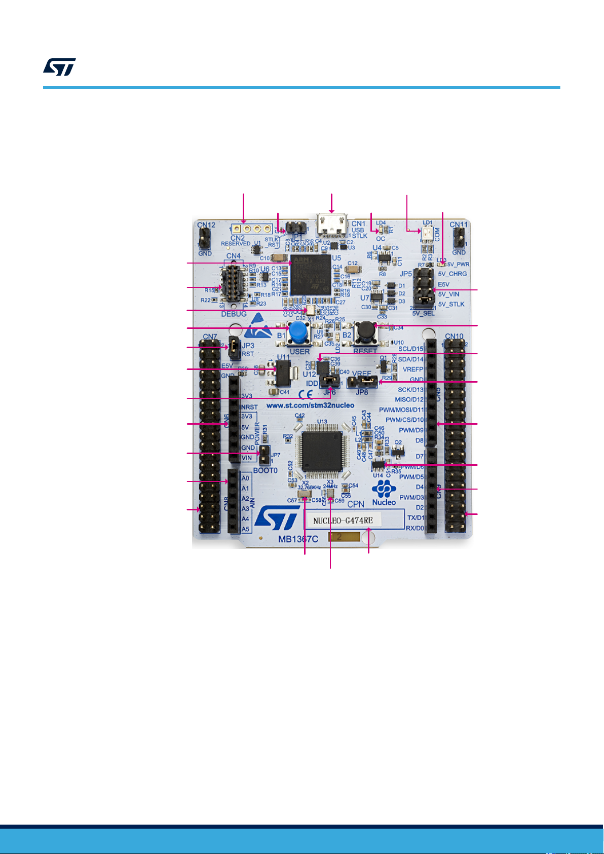
(refer to Figure 4 for component location):
1. Check the jumper position on the board (refer to Table 4)
2. For the correct identification of the device interfaces from the host PC and before connecting the board,
install the Nucleo USB driver available on the www.st.com/stm32nucleo website
3. To power the board, connect the STM32G4 Nucleo-64 board to a PC with a USB cable (Type-A to Micro-B)
through the USB connector CN1 of the board
4. Then, green LED LD3 (5V_PWR) and red LED LD1 (COM) light up, green LED LD2 (USER) blinks
5. Press user button B1 (left blue USER button)
6. Observe how the blinking of the green LED LD2 changes according to the clicks on button B1
7. The software demonstration and the several software examples that allow users exercise Nucleo features,
are available on the www.st.com/stm32nucleo webpage
8. Develop your own application using the available examples
Table 4. Jumper configuration
Jumper Definition Position(1) Comment(1)
JP1 NRST OFF STLINK-V3E reset
JP3 T_RST ON -
JP5 5 V power-source selection
ON [1-2] (Default) 5V_USB_STLK (from ST-LINK)
ON [3-4] (optional) 5V_VIN
ON [5-6] (optional) E5V
ON [7-8] (optional) 5V_USB_CHGR
JP6 IDD ON
JP7 BOOT0 OFF
JP8 VREF+ selection (VREF or VDD
voltage supply selection)
ON [1-2] (Default) VREF+ supplied with VREF
ON [2-3] (optional) VREF+ supplied with VDD
1. Default jumper state is shown in bold.
UM2505
Quick start
UM2505 - Rev 3 page 6/43

6Hardware layout and configuration
The STM32G4 Nucleo-64 board is designed around the STM32 microcontrollers in a 64-pin LQFP package.
Figure 3 shows the connections between the STM32 and its peripherals (STLINK-V3E, push-buttons, LEDs, USB,
ARDUINO® Uno and ST morpho headers). Figure 4 and Figure 5 show the location of these features on the
STM32G4 Nucleo-64 board. The mechanical dimensions of the board are shown in Figure 6.
Figure 3. Hardware block diagram
STLINK-V3E part
STM32G4XXRY
OSC_32
SWD
32 kHz
crystal
VCP
UART
GPIO
GPIOGPIO
Embedded
STLINK-V3E
SWD VCP
UART
USB
Micro-B
connector
(CN1)
B1
button
USER
B2
button
RESET
Arduino™
ST morpho
GPIO
Arduino™
ST morpho
5V
PWR SEL
STLK_RST
GND
GND
DEBUG
BOOT0
VREFIDD
OSC
24 MHz
crystal
xxx
Red LED
LD4 (OC)
Green LED
LD2 (USER)
Green LED LD3
(5V_PWR)
Connectors
or jumpers
Green/Orange LED LD1
(COM)
UM2505
Hardware layout and configuration
UM2505 - Rev 3 page 7/43

6.1 PCB layout
Figure 4. Top layout
LD4 red LED
(Over current)
LD1 bicolor LED
(COM)
LD3 green LED
(5V_PWR)
CN1 STLINK-V3E
Micro-B USB connector
LD4 red LED
(Over current)
JP1
STLINK-V3E reset
CN2
DFU connector
U5 STM32F723IEK6
(STLINK-V3E MCU)
CN4
MIPI10 connector
JP3 Target reset
X1 (25 MHz)
B1 USER button
U11 5V_Vin regulator
LD1117S50TR
JP6
IDD measurement
JP7
BOOT0
CN6
ARDUINO® connector
CN8
ARDUINO® connector
CN7
ST morpho pin header
HW102
product sticker
X2
32 kHz X3
24 MHz
CN9
ARDUINO® connector
CN5
ARDUINO® connector
CN10
ST morpho pin header
U14 voltage ref. IC
TL1431CL5T
JP8
VREF selection
U12 3V3 regulator
LD39050PU33R
JP5 5V power
source selection
B2 RESET button
UM2505
PCB layout
UM2505 - Rev 3 page 8/43

Figure 5. Bottom layout
CN1 STLINK-V3E
Micro-B USB connector
JP1
STLINK-V3E reset
CN2
DFU connector
JP5 5V power
source selection
JP8
VREF selection
JP6
IDD measurement
CN5
ARDUINO® connector
CN9
ARDUINO® connector
CN10
ST morpho pin header
CN8
ARDUINO® connector
CN6
ARDUINO® connector
CN7
ST morpho pin header
JP3 Target reset
CN4
MIPI10 connector
JP7 BOOT0
HW101
board sticker
UM2505
PCB layout
UM2505 - Rev 3 page 9/43

6.2 Mechanical drawing
Figure 6. STM32G4 Nucleo 64 board mechanical drawing (in millimeter)
6.3 Embedded STLINK-V3E
There are two different ways to program and debug the onboard STM32 MCU:
• Using the embedded STLINK-V3E
• Using an external debug tool connected to the CN4 MIPI10 connector.
The STLINK-V3E programming and debugging tool is integrated in the STM32G4 Nucleo-64 board.
UM2505
Mechanical drawing
UM2505 - Rev 3 page 10/43

The embedded STLINK-V3E supports only SWD and VCP for STM32 devices. For information about debugging
and programming features of STLINK-V3, refer to the STLINK-V3SET debugger/programmer for STM8 and
STM32 user manual (UM2448), which describes in details all the STLINK-V3 features.
Features supported on STLINK-V3E:
• 5V power supplied by USB connector (CN1)
• USB 2.0 high-speed-compatible interface
• JTAG/serial wire debugging (SWD) specific features:
– 3 V to 3.6 V application voltage on the JTAG/SWD interface and 5 V tolerant inputs
– JTAG
– SWD and serial viewer (SWV) communication
• Direct Firmware Update (DFU) feature (CN2)
• MIPI10 connector (CN4)
• Status LED LD1 (COM) that blinks during communication with the PC
• Fault red LED LD4 (OC) alerting on USB overcurrent request
• 5 V / 300 mA output power supply capability (U4) with current limitation and LED
• 5 V power green LED LD3 (5V_PWR)
6.3.1 Drivers
Before connecting the STM32G4 Nucleo-64 board to a Windows 7®, Windows 8® or Windows 10® PC via USB,
a driver for the STLINK-V3E must be installed (not required for Windows 10®) . It is available at the www.st.com
website.
In case the STM32G4 Nucleo-64 board is connected to the PC before the driver is installed, some STM32G4
Nucleo-64 interfaces may be declared as “Unknown” in the PC device manager. In this case, the user must install
the dedicated driver files, and update the driver of the connected device from the device manager a shown in
Figure 7.
Note: Prefer using the USB Composite Device handle for a full recovery.
Figure 7. USB composite device
Note: 37xx:
• 374E for STLINK-V3E without bridge functions
• 374F for STLINK-V3E with bridge functions
6.3.2 STLINK-V3E firmware upgrade
The STLINK-V3E embeds a firmware upgrade mechanism for in-situ upgrade through the USB port. As the
firmware may evolve during the lifetime of the STLINK-V3E product (for example new functionalities, bug fixes,
support for new microcontroller families), it is recommended to visit the www.st.com website before starting to use
the STM32G4 Nucleo-64 board and periodically, to stay up-to-date with the latest firmware version.
UM2505
Embedded STLINK-V3E
UM2505 - Rev 3 page 11/43

6.3.3 Using an external debug tool to program and debug the on-board STM32
There are two basic ways to support an external debug tool:
1. Keep the embedded STLINK-V3E running. Power on the STLINK-V3E at first until the COM LED turns red.
Then connect the external debug tool through the CN4 STDC14/MIPI-10 debug connector
2. Set the embedded STLINK-V3E in hig-impedance state: when jumper JP1 (STLK_RST) is ON, the
embedded STLINK-V3E is in RESET state and all GPIOs are in high-impedance; then, connect the external
debug tool to debug connector CN4.
Figure 8. Connecting an external debug tool to program the on-board STM32G4
Table 5. MIPI10 / STDC14 debug connector (CN4)
MIPI10 pin STDC14 pin CN4 Function
- 1 NC Reserved
- 2 NC Reserved
1 3 3V3 Target VCC
2 4 T_SWDIO Target SWDIO using SWD protocol or Target JTMS (T_JTMS) using
JTAG protocol
3 5 GND Ground
4 6 T_SWCLK Target SWCLK using SWD protocol or Target JCLK (T_JCLK) using
JTAG protocol
5 7 GND Ground
6 8 T_SWO Target SWO using SWD protocol or Target JTDO (T_JTMS) using
JTAG protocol
7 9 NC Not connected
UM2505
Embedded STLINK-V3E
UM2505 - Rev 3 page 12/43

MIPI10 pin STDC14 pin CN4 Function
8 10 T_JTDI Not used by SWD protocol, Target JTDI (T_JTDI) using JTAG protocol,
only for external tools
9 11 GNDDetect GND detect for plug indicator, used on SWD and JTAG neither
10 12 T_NRST Target NRST using SWD protocol or Target JTMS (T_JTMS) using
JTAG protocol
- 13 T_VCP_RX Target RX used for VCP (must be UART dedicated to bootloader)
- 14 T_VCP_TX Target TX used for VCP (must be UART dedicated to bootloader)
6.4 Power supply
The power supply can be provided by five different sources:
• A host PC connected to CN1 through a USB cable (default setting)
• An external 7 V - 12 V (VIN) power supply connected to CN7 pin 24
• An external 5 V (E5V) power supply connected to CN7 pin 6
• An external 5 V USB charger (5V_USB_CHGR) connected to CN1
• An external 3.3 V power supply (3V3) connected to CN7 pin 16
UM2505
Power supply
UM2505 - Rev 3 page 13/43

Figure 9. STM32G4 Nucleo-64 board power tree
In case 5V_VIN, E5V, 5V_USB_CHGR, or 3V3 is used to power the STM32G4 Nucleo-64 board, this power
source must comply with the EN-60950-1: 2006+A11/2009 standard and must be Safety Extra Low Voltage
(SELV) with limited power capability.
If the power supply is 3V3, the ST-LINK is not powered and cannot be used.
Power supply input from STLINK-V3E USB connector (default setting)
The STM32G4 Nucleo-64 board and shield can be powered from STLINK-V3E connector CN1 (5 V) by placing a
jumper between pins 1-2 of JP5, “5V_SEL”, as illustrated in Figure 10. This is the default setting.
UM2505
Power supply
UM2505 - Rev 3 page 14/43

Figure 10. Power supply input from STLINK-V3E USB connector with PC (5 V, 500 mA max)
CN1
STLINK-V3E
USB
U5
STM32F723
STLINK-V3E
U4
U12
LDO
3V3
5 V
3V3
PC
< 500 mA
Power switch
5 V
Legend: 5 V 3.3 V
If the USB enumeration succeeds, the 5V_USB_STLK power is enabled, by asserting the T_PWR_EN signal
from STM32F723IEK6 “STLINK V3” (U5). This pin is connected to a power switch STMPS2151STR (U4), which
powers the board. The power switch STMPS2151STR (U4) features also a current limitation to protect the PC in
case of short-circuit on board. If an overcurrent (more than 500 mA) happens on board, the red LED LD4 is lit.
The Nucleo board and its shield can be powered from ST-LINK USB connector CN1, but only ST-LINK circuit gets
power before USB enumeration, because the host PC only provides 100 mA to the board at that time.
During the USB enumeration, the Nucleo board requires 500 mA power from the host PC.
UM2505
Power supply
UM2505 - Rev 3 page 15/43

• If the host is able to provide the required power, the enumeration finishes by a “SetConfiguration” command
and then, the power switch STMPS2151STR is switched ON, the green LED LD3 (5V_PWR) is turned ON,
thus Nucleo board and its shield on it can consume 500 mA at the maximum.
• If the host is not able to provide the requested current, the enumeration fails. Therefore, the
STMPS2151STR power switch (U4) remains OFF and the MCU part including the extension board is not
powered. As a consequence, the green LED LD5 remains turned OFF. In this case, it is mandatory to use an
external power supply.
Caution: If the maximum current consumption of the STM32G4 Nucleo-64 board and its shield boards exceeds 300 mA, it
is mandatory to power the STM32G4 Nucleo-64 board with an external power supply connected to E5V, VIN or
3.3 V.
External power supply input from VIN (7 V - 12 V, 800 mA max)
When the STM32G4 Nucleo-64 board is power-supplied by VIN (refer to Table 6 and Figure 11), the jumper
configuration must be the following: jumper JP2 on pins 3-4 “5V_VIN”.
The STM32G4 Nucleo-64 board and its shield boards can be powered in three different ways from an external
power supply, depending on the voltage used. The three cases are summarized in Table 6.
Table 6. External power sources: VIN (7 V - 12 V)
Input power
name
Connector
pins Voltage range Maximum
current Limitation
VIN CN6 pin 8
CN7 pin 24 7 V to 12 V 800 mA
From 7 V to 12 V only and input current capability is
linked to input voltage:
• 800 mA input current when VIN = 7 V
• 450 mA input current when 7 V < VIN < 9 V
• 250 mA input current when 9 V < VIN < 12 V
UM2505
Power supply
UM2505 - Rev 3 page 16/43

Figure 11. Power supply input from VIN (7 V - 12 V, 800 mA max)
U11
LD1117
S50TR
U12
LDO
3V3
5 V
3V3
VIN < 12 V
Legend: VIN < 12 V 5 V 3.3 V
Refer to Section 6.4.1 for debugging when using an external power supply.
External power supply input from E5V (5 V, 500 mA max)
When the STM32G4 Nucleo-64 board is power-supplied by E5V (refer to Table 7 and Figure 12), the jumper
configuration must be the following: jumper JP5 on pins 5-6 “E5V”.
Table 7. External power sources: E5V (5 V)
Input power name Connector pins Voltage range Maximum current
E5V CN7 pin 6 4.75 V to 5.25 V 500 mA
UM2505
Power supply
UM2505 - Rev 3 page 17/43

Figure 12. Power supply input from 5V_EXT (5 V, 500 mA max)
U12
LDO
3V3
5 V
3V3
Legend: 5 V 3.3 V
Refer to Section 6.4.1 for debugging when using an external power supply.
External power supply input from USB charger (5 V)
When the STM32G4 Nucleo-64 board is power-supplied by a USB charger on CN1 (refer to Table 8 and
Figure 13), the jumper configuration must be the following: jumper JP2 on pins 7-8 “5V_CHGR”.
UM2505
Power supply
UM2505 - Rev 3 page 18/43

Table 8. External power sources: 5V_CHGR (5 V)
Input power name Connector pins Voltage range Maximum current
5V_CHGR CN1 5 V -
Figure 13. Power supply input from ST-LINK USB connector with USB charger (5 V)
CN1
STLINK-V3E
USB
No debug
U12
LDO
3V3
5 V
3V3
USB charger
Legend: 5 V 3.3 V
UM2505
Power supply
UM2505 - Rev 3 page 19/43

External power supply input from external 3.3 V
When the 3.3 V is provided by a shield board, it is interesting to use the 3.3 V (CN6 pin 4 or CN7 pin 16) directly
as power input (refer to Table 9 and Figure 14). In this case, the programming and debugging features are not
available, since the ST-LINK is not powered.
Table 9. External power sources: 3V3
Input power name Connector pins Voltage range Maximum current
3V3 CN6 pin 4
CN7 pin 16 3 V to 3.6 V 1.3 A
UM2505
Power supply
UM2505 - Rev 3 page 20/43
This manual suits for next models
4
Table of contents
Other ST Motherboard manuals

ST
ST X-NUCLEO-IKS01A1 User manual

ST
ST STEVAL-USBPD45H User manual

ST
ST STEVAL-PCC010V1 User manual

ST
ST STR910-EVAL User manual

ST
ST STM32429I-EVAL User manual

ST
ST STM32G0C1E-EV User manual

ST
ST STEVAL-WBC86TX User manual

ST
ST STM3221G-EVAL User manual

ST
ST ST9 Series User manual

ST
ST X-NUCLEO-IDB04A1 User manual