TeleVideo 9320 User manual
TELEVIDEO®
9320 VIDEO DISPLAY TERMINAL
MAINTENANCE MANUAL
Document 133002-00
August 1988
Copyright
Copyright © by TeleVideo Systems, Inc. All rights reserved. No
part
of this publication may
be
reproduced, transmitted, transcribed, storedin a retrievalsystem,
or
translatedinto any language or com-
puter
language, inany form
or
by any means, electronic, mechanical, magnetic, optical, chemical, manual,
or
otherwise, without the prior written permission ofTeleVideo Systems, Inc., 1170 MorseAvenue, P.O.
Box3568, Sunnyvale, California 94088-3568.
Disclaimer
TeleVideo Systems, Inc. makes no representations or warranties with respect to this manual. Further,
TeleVideo Systems, Inc. reserves the right to make changesin the specifications
of
the product described
within this manual at any time without notice and without obligation
of
TeleVideo Systems, Inc. to notify
any person
of
such revision
or
changes.
TeleVideo
is
a registered trademark
of
TeleVideo Systems, Inc.
TeleVideo Systems, Inc., 1170 Morse Avenue, P.O. Box3568, Sunnyvale, California 94088-3568
408/745-7760


Contents
1 Introduction
OVERVIEW
.............................................
1-1
DESCRIPTION
OF
THE
MODULES
..............................
1-2
Logic Circuitry
..........................................
1-2
Video Circuitry
.........................................
1-2
Power Supply Circuitry
.....................................
1-2
Keyboard
.............................................
1-3
RS-423 SIGNALASSIGNMENTS
................................
1-3
SPECIFICATIONS
.........................................
1-4
Physical . . . . . . . . . . . . . . . . . . . . . . . . . . . . . . . . . . . . . . . . . . . . . .1-4
Electrical
.............................................
1-5
Display
.............................................
.1-6
Keyboard . . . . . . . . . . . . . . . . . . . . . . . . . . . . . . . . . . . . . . . . . . . . .1-7
Environmental
..........................................
1-8
CRT
Controller Format
.....................................
1-9
PC
Board
.............................................
1-10
2 Theory ofOperation
INTRODUCTION
.........................................
2-1
DETAILED
DESCRIPTIONS
.................................
.2-2
System Clocking
........................................
.2-2
The GateArray
.........................................
2-2
CPU
System
And
Control
.................................
. .2-2
Character Generation
.....................................
.2-5
Video Display Generation
.................................
. .2-5
Screen
Data
Storage . . . . . . . . . . . . . . . . . . . . . . . . . . . . . . . . . . . . . . .2-6
Communications . . . . . . . . . . . . . . . . . . . . . . . . . . . . . . . . . . . . . . . . .2-6
3 Maintenance
VISUAL INSPECTION
.....................................
.3-1
Terminal and Keyboard Exterior
..............................
.3-1
Terminal and Keyboard Interior . . . . . . . . . . . . . . . . . . . . . . . . . . . . . . .
.3-1
TESTS AND ADJUSTMENTS
....
. . . . . . . . . . . . . . . . . . . . . . . . . . . . .
.3-1
Height
and
Width
.......................................
.3-1
Linearity
............................................
.3-2
Brightness
...........................................
.3-2
Trapezoidal Distortion
....................................
.3-2
Concave and Convex Distortion
...............................
.3-2
Display Stability
........................................
.3-2
iii
Making Adjustments
............................
.........
.3-2
TROUBLESHOOTING
...
. . . . . . . . . . . . . . . . . . . . . . . . .
..........
3-3
REMOVING
THE
MODULES
.................................
.3-5
Opening the Case
............................
...........
.3-5
Removing the Circuit Board
.................................
.3-6
Replacing the Circuit Board
.................................
.3-6
Closing the Terminal Case
..................................
.3-8
Opening the Keyboard Case and Removing the Keyboard Circuit . . . . . . . . . . . . .3-8
Replacing the Keyboard Circuit and Closing the Keyboard Case
............
.3-8
4 Parts and Service
ORDERING
SPARE
PARTS
........
;
.........................
.4-1
SERVICEINFORMATION
...................................
.4-8
Return Procedure
..............
. . . . . . . . . . . . . . . . . . . . . . . . . .4-8
Regional Sales Offices
....................................
.4-8
5 Schematics
A Service Bulletins
Illustrations
1-1
Front View
of
the 9320
..
1-2
Rear
View
of
the 9320 . . . . . .
1-3
Keyboard Layout . . . . . . .
2-1 Block Diagram
of
the 9320 .
2-2 Memory Map for the 9320 .
3-1 Discharging Voltages
....
3-2 Opening the Terminal Case .
3-3 Removing
the
Circuit Board
Tables
1-1
Main Port Assignments for DB-25
....
1-2 Main Port Assignments for DECconnect
1-3
Printer Port Assignments for DB-25
....
1-4 Printer PortAssignments for DECconnect
3-1 Troubleshooting Guide .
4-1
Main Parts List
..
. . . . . . . . . . . . . . .
4-2 Parts Reference List
............
.
5-1 Circuit Board
IC
Reference (Logic Board)
iv
· .1-1
· .1-2
.1-7
· .2-1
· .2-3
.3-5
.3-6
.3-7
.1-3
.1-3
.1-3
.
.....
1-3
......
3-3
.4-1
.4-2
.
..
5-1
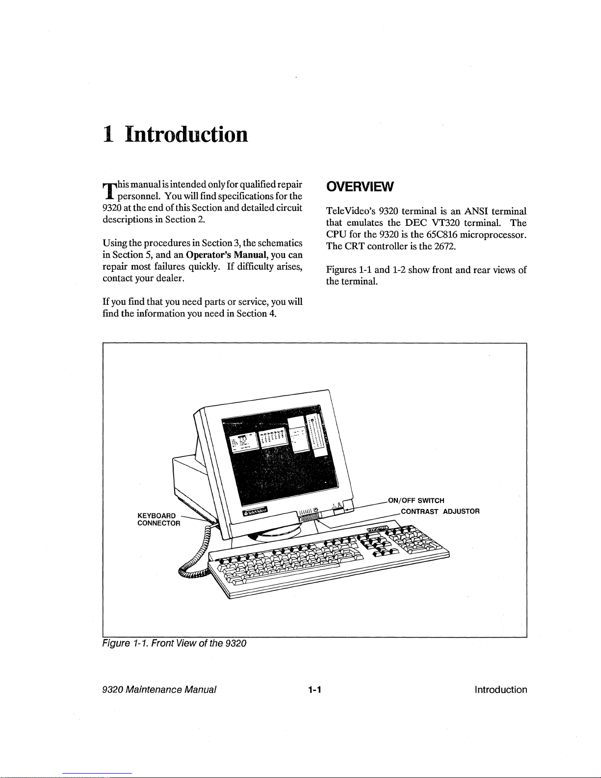
1 Introduction
Thismanualisintendedonlyforqualifiedrepair
personnel. Youwill find specifications for the
9320 at
the
end
of
thisSectionand detailedcircuit
descriptions in Section
2.
Using
the
proceduresinSection
3,
theschematics
inSection
5,
and
an
Operator's
Manual, you can
repair most failures quickly.
If
difficulty arises,
contact your dealer.
If
you fmd thatyou
need
parts or service, youwill
fmd the informationyou
need
in Section
4.
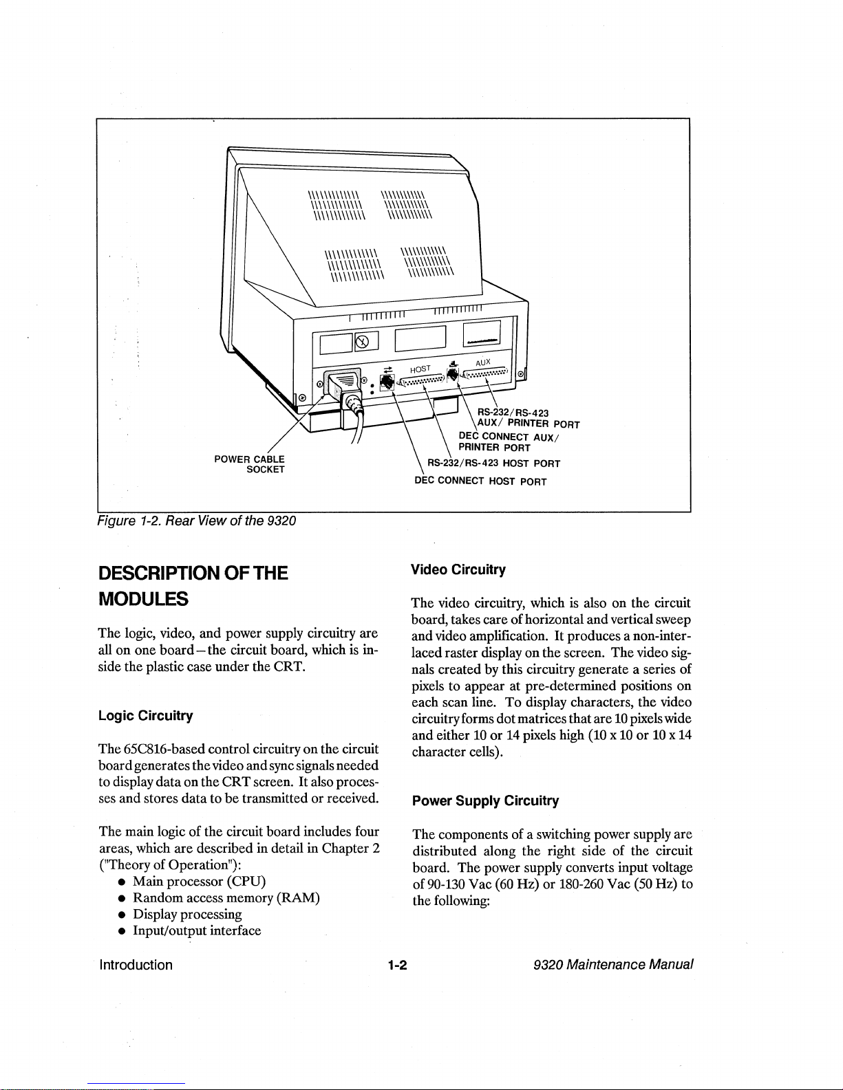
Figure 1-1. FrontView
of
the 9320
9320 Maintenance Manual
1-1
OVERVIEW
TeleVideo's 9320 terminal is
an
ANSI terminal
that emulates the
DEC
VT320 terminal.
The
CPU
for the 9320 is
the
65C816 microprocessor.
The CRT controller is the 2672.
Figures 1-1
and
1-2 show front and
rear
views
of
the terminal.
Introduction
\\\\\\\\\\\\\
\\\\\\\\\\\\\
\\\\\\\\\\\\\
\\\\\\\\\\\\
\\\\\\\\\\\\
\\\\\\\\\\\\
\\\\\\\\\\\\\
\\\\\\\\\\\\\
\\\\\\\\\\\\\
\\\\\\\\\\\\
\\\\\\\\\\\\
\\\\\\\\\\\\
-__
-----=::-,!!,.
AUX
~a~~~'-:-i-n~=~/:~4~
AUX/
PRINTER
PORT
DEC
CONNECT
AUX/
PRINTER
PORT
POWER
CABLE R5-232/RS.423 HOST PORT
SOCKET
Figure 1-2. RearView
of
the 9320
DESCRIPTION
OF
THE
MODULES
The logic, video,
and
power supply circuitry
are
all
on
one
board
-the circuit board, which is in-
side the plastic case under the CRT.
Logic
Circuitry
The65C816-based control circuitry
on
the circuit
board
generatesthevideo
and
syncsignalsneeded
to display
data
on the
CRT
screen.
It
also proces-
ses
and
stores
data
to
be
transmitted
or
received.
The main logic
of
the circuit board includes four
areas, which
are
described in detail in Chapter 2
("Theory
of
Operation"):
• Main processor (CPU)
•
Random
access memory (RAM)
• Display processing
• Input/output interface
Introduction 1-2
DEC
CONNECT
HOST
PORT
Video
Circuitry
The
video circuitry, which is also
on
the circuit
board, takes care
of
horizontal
and
verticalsweep
and
video amplification.
It
producesa non-inter-
lacedraster display
on
the screen.
The
video sig-
nals created by this circuitry generate a series
of
pixels to appear
at
pre-determined positions
on
each scan line.
To
display characters, the video
circuitryforms dotmatricesthat
are
10
pixelswide
and
either
10
or
14 pixels high (10 x
10
or
10
x 14
character cells).
Power
Supply
Circuitry
The
components
of
a switching power supply
are
distributed along
the
right side of the circuit
board. The power supply converts input voltage
of90-130 Vac (60 Hz)
or
180-260
Vac
(50 Hz) to
the following:
9320 Maintenance Manual
+5 Vdc for TTLlogic
on
the circuit board
+12Vdcfor thevideo signals andRS-423 com-
munications
-12
Vdc for RS-423 communications
A user-replaceable fuse near the power plug
protects the circuitry from excess current.
Keyboard
The
9320
has a detachable keyboard connectedto
theterminal
by
a coiled cable. Thiskeyboard con-
tainsanarrayofkeyswitchesmountedonaprinted
circuit
board
(PCB)
that
includes
an 8049
microcontroller and other components.
The
8049
scans the keyboard matrix, encodes the
data, and transmits the appropriate scan codes.
Data
is
transmittedthrough a4-wire cableover an
asynchronous serial port at
9600
baud to the main
logic board.
On the circuit board, the serial data
is
converted
to parallel and decoded by the main processor
using decoding firmware.
RS-423 SIGNAL
ASSIGNMENTS
Main Port Connectors
The
9320
has two RS-423 main port connectors:
one
DB
25-pin
(labeled
HOST)
and
one
DECconnect (labeled
~).
Table 1-1. Main
Port
Assignments for
DB-25
Pin Signal Name Direction
1 Frame Ground nla
2 Transmit
Data
Output
3 Receive Data Input
4 Request to Send Output
5 Clear to Send Input
9320 Maintenance Manual 1-3
6
7
8
20
Data
Set Ready
Signal Ground
Data
Carrier Detect
Data
Terminal Ready
Input
n/a
Input
Output
Table
1-2.
Main
Port
Assignments
for
DECconnect
Pin Signal Name Direction
1
Data
Terminal Ready nla
2 Transmit
Data
Output
3 Transmit Signal Ground Input
4 Receive Signal Ground Output
5 Receive
Data
Input
6
Data
Set Ready Input
Printer Port Connectors
The
9320
has two RS-42J printerport connectors:
one
DB
25-pin
(labeled
AUX)
and
one
DECconnect (labeled.!,).
Table 1-3. Printer
Port
(DCE) Pin Assignments
Pin Signal Name Direction
1 Frame Ground nla
2 Receive Data Input
3 Transmit
Data
Output
5 Clear to Send Output
6
Data
Set Ready Output
7 Signal Ground nla
8
Data
Carrier Detect Output
20
Data
TerminalReady Input
Table
1-4.
Printer
Port
Assignments
for
DECconnect
Pin Signal Name Direction
1
Data
Terminal Ready n/a
2 Transmit
Data
Output
3 Transmit Signal Ground Input
4 Receive Signal Ground Output
5 Receive
Data
Input
6
Data
Set Ready Input
Introduction

SPECIFICATIONS
Physical
VDT Dimensions:
Height
Width
Depth
VDT
NetWeight
Case Foot Print
Case Features:
Tilt
Swivel
Cooling
Connectors
CRT:
Diagonal Measure
Phosphor
Fluorescence
Bulb
Face-plate
Screen
Persistence
Introduction
13.6 inches (34.5 cm)
12.9 inches (32.8 cm)
13.9 inches (35.4 cm)
17.5lbs.
8.6 inches by 8.0 inches (max.)
-5
to +
15
degrees
2700 left to right
Convection system
One RS423 communication
port
(DB25 male and
RJll
DECconnect)
One RS423 printer port (DB25 female and
RJll
DECconnect)
One
RJll
keyboard
port
One
AC
receptacle-type quick disconnect
13.7 inches (34.8 cm)
P134 (amber); P192 (paper white)
Amber;
paper
white
90
0 deflection,
60"
radius face
Filterglass
Aluminized
Medium short (300us decay time)
1-4 9320 Maintenance Manual
Electrical
ACSupply:
Input
Line Voltage
(Jumper Selectable)
Frequency
Source Current:
115VLine
230VLine
Phase
Wattage
DC
Supply:
SV
12V
-12V
Ripple
and
Spike Noise
9320 Maintenance Manual
95Vto
130V
180Vto260V
50/60
Hertz
+
/-
3 Hz.
1.0
Amp
max.
0.5
Amp
max.
Single phase, 3-wire
40
VA
max.
+/- .2SVat 1.5
Amp
+
/-
.24V at 1.6
Amp
+
/-
.24V at 150mA
SOm
V peak to
peak
+5V
100mV peak
to
peak
+12V; -12V
1-5 Introduction
Display
HorizontalScanning Frequency
Vertical Scanning Frequency
Character Lines
Columns
Per
Line
Cell Size (Character Block):
Width
Height
High Voltage
(At
Dark
Screen)
High Voltage Regulation (From Dark
Screen to Full Bright)
Picture Brightness at Maximum Contrast
Adjustment
Equal
to
or
Greater Than
Picture Size (Active Display):
Format
Width
Height
Levels
of
Gray
Introduction
80 132
26.46 Khz 26.46 Khz
70Hz,
80Hz
70Hz,
80Hz
24,25 24,25
80 132
Dot
Matrix
Dot
Matrix
10
10
14,
10
14,10
13.5 KV +
/-
500V 13.5 KV +
/-
500V
500V
+/-
250V
20
ft.
Lambert
24,
25
lines
240mm
180mm
Dark, HalfBright,
FullBright
1-6
500V
+/-
250V
20
ft. Lambert
24,
25 lines
240mm
180mm
Dark,
Half
Bright,
Full Bright
9320 Maintenance Manual
)
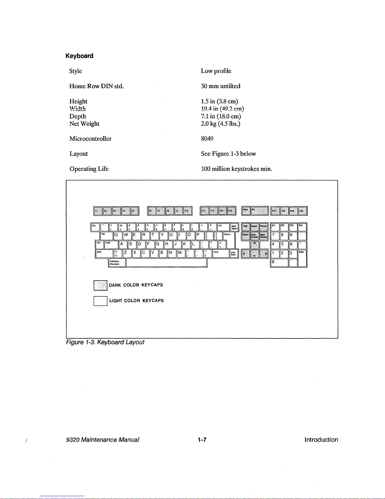
Keyboard
Style
Home
Row
DIN
std.
Height
'Nidth
Depth
Net
Weight
Microeontrol1er
Layout
Operating
Life
D DARK COLOR KEYCAPS
D LIGHT COLOR KEYCAPS
Figure 1-3. Keyboard Layout
9320 Maintenance Manual
Low
profile
30
mm
untilted
1.5 in (3.8 em)
1QLl
in
(LlQ?
r,m)
--
..
---
'-
-_.-
---/
7.1
in
(18.0 em)
2.0 kg (4.5 lbs.)
8049
See
Figure 1-3
below
100 million keystrokes min.
1-7 Introduction
Environmental
Operating:
Temperature
Humidity
Altitude
Non-operating:
Temperature
Humidity
Altitude
MTBF
MTTR
Vibration
Shock
Shipping:
Girth
Weight
Introduction
5 to
40°
C (41
to
104°
F)
10 to
85%
non-condensing
3,000 m (10,000 ft.)
-40
to
60°
C (-40
to
140°
F)
10
to
85%
5,000 m (15,000 ft.)
20,000 hours min.
15 minutes
0.3G, 5 to 100 Hz., operational
2OG,
Ums,
18 shocks
108 inches max.
50 lbs. max.
1-8
9320
Maintenance Manual <
CRT
Controller
Format
80x26
132x26
Dot
Frequency 26.9892
MHz
44.4528
MHz
Character Cell:
Number
of
Dots per Character (Width)
10
10
Number
of
Scan Lines per Character (Height) 10,14 10,14
Character Frequency 2.6989 MHz 4.4452
MHz
ScreenFormat:
Display Characters
per
Line
80
132
Total Characters
per
Line 102
168
Number
of
Rows
per
Screen
25 25
/ 9320 Maintenance Manual 1-9 Introduction

PC Board
Main Features:
Type
of
board
Microprocessor
CRT
Controller
Communication controller
Gate Array
Battery
Current Load:
Standard
with Options
Memory
System
ROM
System
RAM
(CMOS)
Display
RAM
Charactergenerator
RAM
Communications:
Main Port
Printer Port
Parity
Data
Bits
Handshaking
Introduction
2-sided, includes power
and
ground
65C816 (5 MHz)
2672
(5
MHz)
2681
DUART
PIN 271049-00 (custom)
3V min. Lithium
1.2A (5V); 1.5A (12V); 100 rnA (-12V)
1.5A (5V) max.
64K (27512)
8Kbytes
16K x 2 (character
and
attribute)
8Kbytes
RS423 (P3, P6) (75 -19.2K bit/sec.)
RS423 (P4, P5) (75 -19.2K bit/sec.)
No, Odd, Even, Mark, Space
7or8
No, X-on/X-off, DTR, both
1-10 9320 Maintenance Manual \
2 Theory
of
Operation
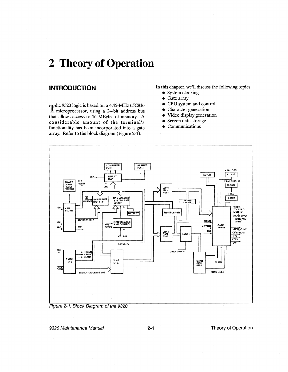
INTRODUCTION
T
he
9320 logic
is
based
on a 4.45-MHz 65C816
microprocessor, using a 24-bit address bus
that allows access to 16 MBytes
of
memory. A
considerable
amount
of
the
terminal's
functionality has
been
incorporated into a gate
array. Refer to the block diagram (Figure 2-1).
~
CPU
65C816
HMI
HSYNC
VSYNC
BLANK
DISPLAY ADDRESS BUS
DATABUS
MUX
5157
Figure 2-1. Block Diagram
of
the 9320
9320 Maintenance Manual 2-1
In
this chapter, we'll discuss the following topics:
• System clocking
~
Gate
array
•
CPU
system
and
control
• Character generation
• Video display generation
• Screen
data
storage
• Communications
CHAR LATCH
CHAR
GEN
6264 1
BLANK
SCAN LINES
Theory
of
Operation
DETAILED
DESCRIPTIONS
System Clocking
The
9320
displays
lO
x
14
character cells in either
SO-column
or 132-colurnn mode, using a different
dot clock for each display mode. Clock oscillator
Y2 at
44.4528
MHz serves
as
the basic. clock in
.132-column mode. A crystal circuit (Y3), which
oscillatesat
26.9S92
MHz, servesas thebasicclock
in
SO-column
mode. (Crystal
Y1
serves
as
a baud
rate clock for the communication ports.)
Selection of
80
or
132
column operation
is
done
inside
the
gate array chip through software
programming.
The
frequency at which the
microprocessor operates depends on the mode of
operation selected,
80
or
132
column. Oscillator
Y2
the dot clock in132-column mode, serves as a
clo~k
to send video data through a shift register
inside the gate array, and serves as a processor
clock after it
is
divided by ten. Crystal oscillator
Y3
the
dot clockin
80
columnmode, provides the,
same two functions.
The Gate Array
Themajorfunctions ofthegatearrayincludebasic
timing functions, reading and writing attribute
RAM, timing for writing to various areas of
memory,
control
for
the
character
RAM
transceiver, font-loading, various scan line func-
tions, keyboard communication, and handling
video attributes and the video shift registers.
Descriptions are given in the paragraphs that fol-
low.
The CPU clock
is
stretched in
132
column mode
when accessing the
EPROM
and CRTcontroller.
The system clock
is
also stretchedwhen accessing
I/O ports in both modes. The CRT controller
character clock
is
the inverted system clock. The
baudrate clock generator circuit for the I/O ports
is
also generated inside the gate array.
The gate array controls attribute RAM data
read/write
operation.
The
gate
array also
provides a write pulse for screen
RAM
and
Theory of Operation 2-2
character generator RAM, address decode for
EPROMs, screen RAM, I/O ports and other sig-
nals.
It
provides a control signal to control.the
direction of the character RAM transceiver.
Thegate arrayloads fonts to the character gener"
ator. Fourofthescanaddresslines comefrom the
gate array. The scan line counter that
contr~ls
doublewidth, double height and smooth scrollIng
is
also inside.
In
addition, the gate array handles keyboard
transmit and receive data, attributelogic, andthe
video shift register.
The CPUcommunicates with the gate array using
internal registers that are accessed
by
reading or
writing specific locations inside the gate array.
One status register (read only) provides the CPU
with the status of internal signals like transmit
register empty, receiver
full,
keyboard overflow,
and interrupt.
CPU System And Control
The CPU system consists of the following four
subsystems (with identifiers from sheet 1 of the
schematics in parentheses):
• the
65C816
CPU (U14)
• the system
27512
EPROM (U12)
• the
6264
system RAM (U13)
• the system reset controller (UlO)
TheCPU
is
the controllerfor the entireboard,in-
itializing and controlling all of the DUART, the
CRT controller, the clock circuits and the gate
array.
It
also processes all of the data received
from the keyboard, computer, orprinter, and up-
dates the video RAM accordingly.
The CPU address space
is
divided into
256
banks
of
64
Kbytes.
It
always
readsinstructions from the
EPROM. Data
is
read from
EPROM
U12 as
from bank 1 and EPROM U11 as from bank
3.
Many of the display features, such as smooth
scrolling and line lock are controlled
by
the CPU
in conjunction with the CRT controller and gate
array.
9320 Maintenance Manual
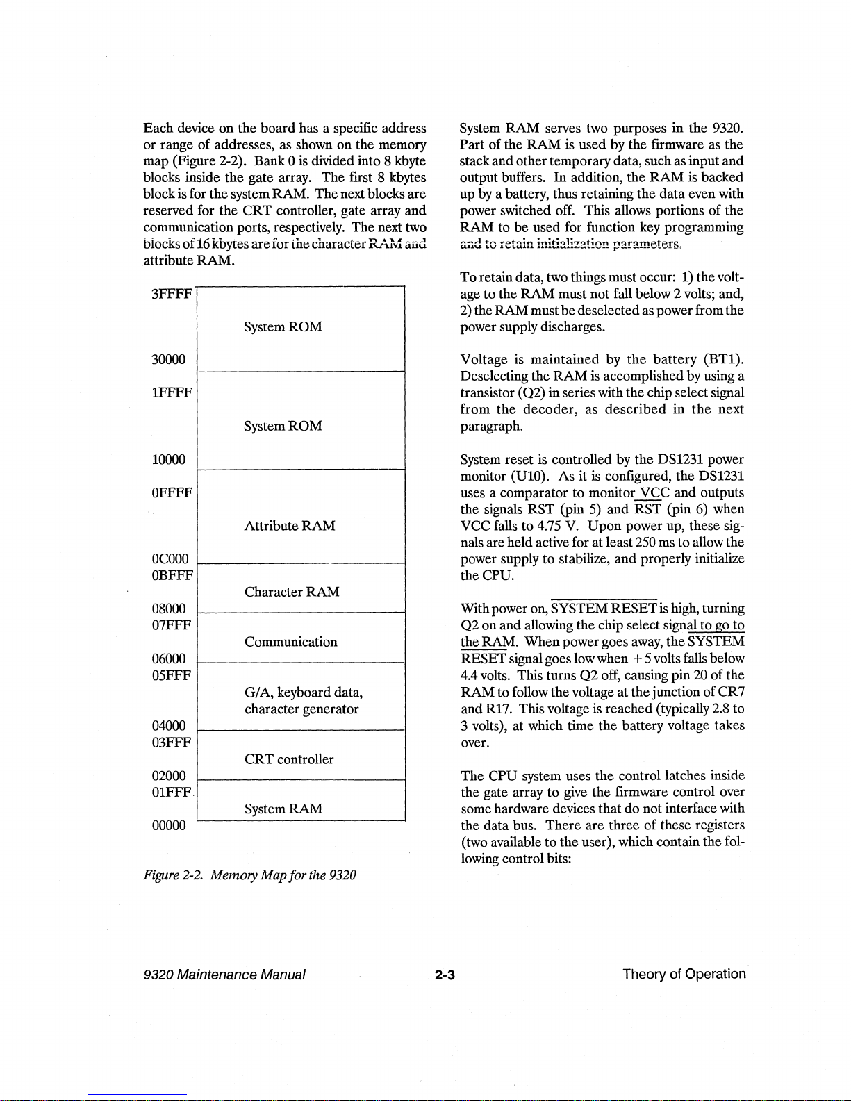
Each device on the
board
has a specific address
or range of addresses, as shown on the memory
map (Figure 2-2). Bank 0
is
divided into 8 kbyte
blocks inside the gate array. The first 8 kbytes
blockis for the systemRAM. Thenext blocks are
reserved for the CRT controller, gate array and
communication ports, respectively. The next two
biocks of
i6
kbytes arefor ihecharacteI'
RAIvf
aiid
attribute RAM.
3FFFF
30000
1FFFF
10000
OFFFF
OCOOO
OBFFF
08000
07FFF
06000
05FFF
04000
03FFF
02000
01FFF
00000
System
ROM
System
ROM
Attribute
RAM
Character
RAM
Communication
G/A, keyboard data,
character generator
CRT
controller
System
RAM
Figure
2-2.
Memory
Map
for
the 9320
9320 Maintenance Manual 2-3
System
RAM
serves two purposes in the 9320.
Part of the
RAM
is used by the firmware as the
stackand othertemporary data, such as input and
output buffers.
In
addition, the
RAM
is backed
up
by a battery, thus retaining the data even with
power switched off. This allows portions of the
RAM
to be used for function key programming
and
to
retain
initia!ization parameters.
Toretain data, two things must occur: 1) the volt-
age to the
RAM
must not fall below 2 volts; and,
2) the RAMmust
be
deselectedas power from the
power supply discharges.
Voltage is maintained
by
the
battery
(BTl).
Deselecting the
RAM
is
accomplished
by
using a
transistor
(02)
inserieswith the chip select signal
from
the
decoder,
as
described
in
the
next
paragraph.
System reset is controlled by the DS1231 power
monitor (UlO). As it
is
configured, the DS1231
uses a comparator to monitor VCC and outputs
the signals RST (pin 5) and RST (pin 6) when
VCC falls to
4.75
V.
Upon
power up, these sig-
nals are held active for at least250 ms to allow the
power supply to stabilize, and properly initialize
the cpu.
Withpower on, SYSTEM
RESET
is high, turning
02
on and allowing the chip select signal to go to
the RAM. Whenpower goes
away,
theSYSTEM
RESETsignal goes lowwhen +5volts falls below
4.4 volts. This turns
02
off, causing pin
20
of the
RAM
to follow the voltage at thejunctionofCR7
and R17. This voltage
is
reached (typically 2.8 to
3 volts), at which time the battery voltage takes
over.
The CPU system uses the control latches inside
the gate array to give the firmware control over
some hardware devices that do not interface with
the data bus.
There
are three of these registers
(two available to the user), which contain the fol-
lowing controlbits:
Theory of Operation
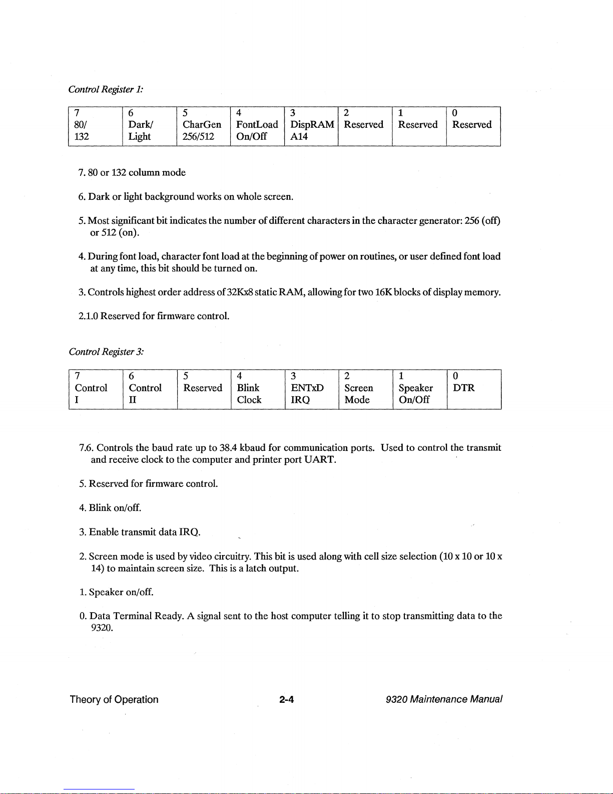
Control Register
1:
7 6 5 4 3 2 1 0
80/ Dark! CharGen FontLoad DispRAM Reserved Reserved Reserved
132 Light 256/512 On/Off A14
7.80
or
132 column mode
6.
Dark
or
light background works
on
whole screen.
5.
Most significantbitindicates the number
of
different charactersin the charactergenerator:
256
(oft)
or
512 (on).
4.
Duringfont load, characterfont load at thebeginning
of
power
on
routines,
or
user defined font load
at any time, this bit should
be
turned on.
3.
Controlshighest order address
of
32Kx8 staticRAM, allowing for two 16Kblocks
of
displaymemory.
2.1.0 Reserved for firmware control.
Control Register
3:
7 6 5 4 3 2 1 0
Control Control Reserved Blink ENTxD Screen Speaker
DTR
I
II
Clock
IRQ
Mode On/Off
7.6. Controls the
baud
rate up to 38.4 kbaud for communication ports.
Used
to control the transmit
and
receive clock to the computer and printer
port
UART.
5.
Reserved for firmware control.
4.
Blink on/off.
3.
Enable transmit data IRQ.
2.
Screen mode
is
used by video circuitry. This bit is used along with cell size selection (10 x 10
or
10
x
14) to maintain screen size. This
is
a latch output.
1.
Speaker on/off.
o.
Data
Terminal Ready. A signal sent to the host computer telling it to stop transmitting data to the
9320.
Theory of Operation 2-4 9320 Maintenance Manual
Character
Generation
The 9320 uses character cells, rather than a full
bit-mapped display, to produce characters on the
screen.
In
24-25 row mode, each character cell
is
10
pixels wide by 14 pixels high. The screen dis-
plays either 3300 character cells in 132-column
mude (132 A 25),
or
2000 character cells
in
80-
column mode (80 x25).
Each
ofthe
512
possible characters
is
pre-defmed
and
resides in the character generator
RAM
(U34). (Duringpower-up, thecharacter fonts are
copied from
EPROM
to character generator
RAM.) The
CPU
changes the display by chang-
ing the code stored in the screen RAMS at the
desired location(s).
The codes written into the screen RAM are read
out as the CRT controller refreshes the display
(see "Video Display Generation" later in this
chapter). As each code
is
read out, one per
characterclock cycle, itis latchedintothe charac-
ter address latch (U35).
The outputs of the character address latch are
usedas thehigh order address lines ofthe charac-
tergeneratorRAM. Thelow-orderaddresses are
providedby the scan line counter inside the gate
array. The 8-bit data from the character gener-
ator
is
transformed into lO-bit words inside the
gate array.
In
order to load the character generator RAM,
the following circuits are provided inside the gate
array. The scan line counter
is
loadable by the
CPU
via the scan line offset register, which
is
ac-
cessed as one
of
the registers in the gate array.
It
is loaded with data present on
DO-D3
outputs of
the
scan
line offset register. During normal
operation, this counter
is
clocked by BLANK.
During font load, it
is
clocked by accesses to the
character generator data register.
During screen refresh, data is transferred from
thescanline offsetregisterto thescanlinecounter
on the rising edge of BLANK from the CRTC.
During a font
load
operation, the transfer does
not occur.
9320 Maintenance Manual 2-5
Under
certain
conditions,
two
of
the
shift
register's inputs
are
connected to provide a
character cell 10 pixels wide without using a spe-
ciallO-bit wide RAM.
In
normal text mode, D7
from the character generator
is
always a low
(zero), creating a single dot space on the left side
ofeach character cell.
Video
Display
Generation
Thevideomonitor requires threesignals from the
logic board to produce a display on the CRT:
• vertical sync (VSYNC)
• horizontal sync (HSYNC)
• video (VIDEO)
VSYNC and HSYNC originate from the CRT
controller (U15). They arebuffered and connect
to the video section of the board. Video comes
from the gatearray (U26).
It
goes through a high-
current
open
collector inverter (U20), where
DEC
and
HI
outputs are also tied.
HSYNC and VSYNC aretimed pulses derivedby
the CRT controller from internal programmable
counters that count CCLK cycles.
For
example,
HSYNC might
be
a positive-going pulse starting
83
CCLK cycles after the beginning ofeach scan
line and lasting
18
CCLK cycles. The
CRT
con-
troller's internalcounterwould reset atthebegin-
ning of each scan line, count to
83,
set HSYNC
high, count
18
more CCLKs andset HSYNC
low.
VSYNC is a much slower signal based on scan
lines. Another counterinside the
CRT
controller
counts scari lines and toggles VSYNC according
to the
way
the firmware has prpgrammed the in-
ternal registers.
As the SCN2672 CRT controller (U15) counts
CCLKs, it
is
also putting out addresses on its dis-
play
address
lines
(pins
21-34,
DAD
DO-
DADD13). These lines connect to four 74LS157
4-bit, two-waymultiplexers (U18, U22-U24). The
selectinputs
of
themultiplexers arenormallyhigh,
allowing the
CRT
controller's address line to ac-
cess the data in the screen RAMs.
Theory
of
Operation
Table of contents
Other TeleVideo Desktop manuals

TeleVideo
TeleVideo 950 User manual

TeleVideo
TeleVideo TS 802H User manual

TeleVideo
TeleVideo TS 806/20 User manual

TeleVideo
TeleVideo 955 User manual

TeleVideo
TeleVideo TS 806H User manual

TeleVideo
TeleVideo TS-1605 User manual

TeleVideo
TeleVideo 925 User manual

TeleVideo
TeleVideo TVI-9128 User manual

TeleVideo
TeleVideo TPC I SYSTEM User manual
Popular Desktop manuals by other brands


HP
HP Visualize c200 - Workstation install guide
 user guide")
Sony
Sony PCG-SRX99K VAIO User Guide (primary manual) user guide

Twoey Outside
Twoey Outside 9750 Assembly instructions

Lenovo
Lenovo ThinkStation E31 Manual do utilizador

Digital Equipment
Digital Equipment VAXstation 2000 owner's manual

HP
HP dc72 - Blade Workstation Client user manual