73S1215F Evaluation Board User Guide UG_1215F_039
20 Rev. 1.8
4.2 Test Points
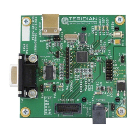
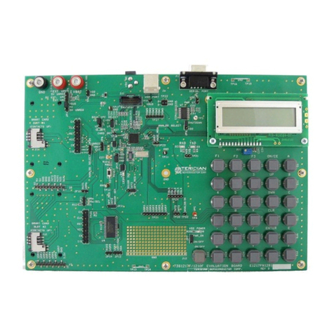
The test point numbers listed in Table 3refer to the test point numbers shown in the electrical schematic
and in the silkscreen of the PCB.
Table 3: Evaluation Board Test Point Description
Test
Point # Name Use
TP2, TP3 +3.3V +3.3 V main board power supply, coming from the internal or external
source, as defined from the jumpers JP3 and JP6. TP3 and TP4 are close
to the breadboard area for easy wiring of the power supply.
TP6
VDD
2-pin test point, with one ground and one VDD signal directly connected to the
73S1215F and its decoupling capacitors. Can be used to measure the integrity
of thedigital power supply of the 73S1215F, or to add a decoupling capacitor.
TP7
VPC
2-pin test point, with one ground and one VPC signal directly connected to
the 73S1215F and its decoupling capacitors. Can be used to measure the
integrity of the power supply of the DC-
DC converters of the 73S1215F, or to
add a decoupling capacitor.
TP8 +5V +5 V coming from either the USB bus or from the external DC block (connected
to JP5), as selected with jumper on JP1. Can be used to test voltage presence.
TP9 +3.3VFIX +3.3 V coming from the on-board regulator (powered from either the USB
bus or the external DC block). Can be used to test voltage presence.
TP10 Smart Card
Contacts –
Interface #1
Header for measurement of the card signals, close to the card connectors.
Contains the card signals VCC1, RST1, CLK1, C81 and C41. Each contact
has its own ground pin on the header.
TP11 to
TP17 GND Ground test points. Can be used for grounding of lab equipment probes.
TP18 Card Detect –
Interface #1 Card detect signal coming directly from the card connectors.
TP21 USR(8:0) Standard 9/8-bit user I/O port of the 73S1215F.
Some of the user I/Os are shared by the LCD interface and the
extension 73S80xx daughter board when using additional external
smart card interfaces.Only one should be used at a time.
TP22 USB TP22 has 4 pins, connected to the USB D+ and D- wires, as well as 2 grounds.
TP24 VBUS +5V USB bus. Can be used as a test point for USB voltage presence.
TP25 Smart Card
Contacts –
Interface #2
Header for measurement of the card signals, close to the card connectors.
Contains the card signals VCC2, RST2, CLK2, C42 and C82. Each contact
has its own ground pin on the header.
TP26 INT3 Interrupt input #3 secondary test points.
TP27 ROW[0:5] The row pins used for the keypad interface.
TP28 LED0-4 The LED outputs from the 73S1215F.
TP29 COL[0:4] The column pins used for the keypad interface.
TP30 INT2-3 Interrupt input #2 and #3 of the 73S1215F. This header is close to the
breadboard area for easy wiring.
TP31 RX, TX The TX and RX serial UART I/O signals (3.3 V digital logic level).
TP32 ANALOG IN Analog input test point. Analog voltage can be connected to this test point
for voltage comparison.
TP34 CPUCLK This pin outputs the oscillator clock of the 73S1215F device. Can be used
as a clock source for any purpose.
Downloaded from: http://www.datasheetcatalog.com/


