A-Trend ATC-2000 User manual

Table of Contents
JUMPER & CONNECTOR LOCATION DIAGRAM.............A
CHAPTER 1 INTRODUCTION..........................................2
1-1 SYSTEM FEATURES.........................................................3
1-2 CHECK LIST OF THE PACKING........................................4
CHAPTER 2 INSTALLATION...........................................5
2-1 INSTALLATION PROCEDURES .......................................5
2-2 CPU INSTALLATION..........................................................6
2-3 SYSTEM MEMORY INSTALLATION..................................11
2-4 SRAM INSTALLATION.......................................................13
2-5 OTHER JUMPERS AND CONNECTORS
DESCRIPTION ..................................................................14
2-6 IDE DRIVER INSTALLATION.............................................1
CHAPTER 3 AWARD BIOS SETUP.................................20
3-1 UPDATE BIOS PROCEDURES..........................................21
3-2 AWARD SYSTEM BIOS CONFIGURATION SETUP.........22
APPENDIX A ......................................................................46

CHAPTER 1 INTRODUCTION
This manual introduces how to configure the ATC-2000 mainboard for
different environments. It's an overview of the layout and features of the
mainboard, and also rovides information for
you to change the configuration or system environment.
This manual is divided into two sections :
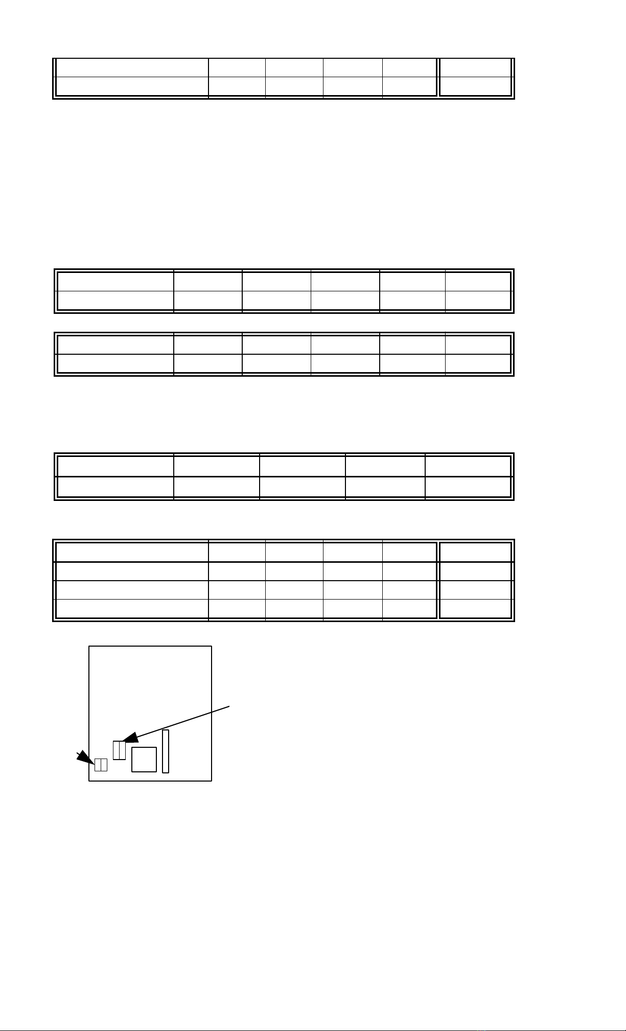
PART ONE includes age A which contain layout diagram of
the mainboard. Please refer it when you configure the system.
PART TWO includes three cha ters as following:
Cha ter 1 is an overview of the mainboard features and acking
contents of the mainboard.
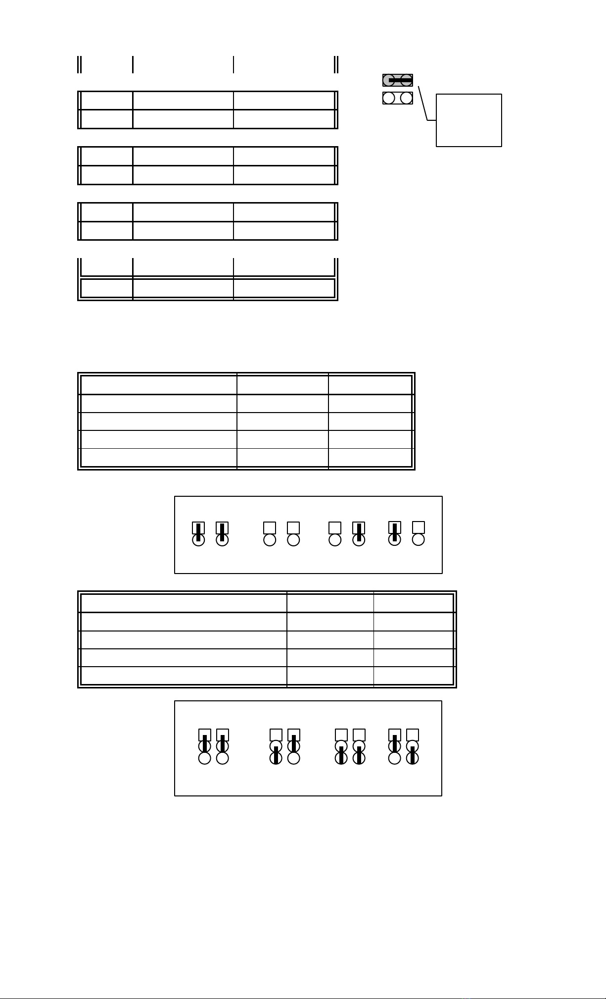
Cha ter 2 describes how to u grade and to change hardware
configurations such as memory size, CPU ty e, and lists of
jum er settings and connectors.
Cha ter 3 is the user's guide of AWARD BIOS setu utility,
and Flash ROM BIOS u date rocedure. The menu showed in
this cha ter are default settings.
Your system dealer will set u the mainboard according to your
demand of com uter. It means that the current settings of your
mainboard's current setting may not be the same as the defaults shown
in this user's manual. If you need to change your
configuration, lease ask your dealer firstly, be sure this will not
against your system warranty. Or ask for your dealer to do it for you.
REMARK
Intel® is a registered trademark of Intel Cor oration.
MS-DOS® is a registered trademark of Microsoft Cor oration.
All other brands and roduct names are trademarks registered trademarks of their res ective
com anies.
1-1 SYSTEM FEATURES
:P54C, P55C Pentium level CPU o erating at 75 MHz to 200MHz with
321- in ZIF socket 7 and scalability to acce t rocessor in the
future.
:INTEL 82430HX PCIset.
:Using four 72- in SIM sockets, rovides two banks of 64-bit wide ath
u to 256MB addressing age mode DRAMs.

:Su orting all ty es of DRAM included ECC (Error Checking and
Correcting) or arity, EDO (Extended Data Out), BEDO (Burst EDO),
or FPM (Fast Page Mode).
:Su orting four PCI bus master revision 2.1, 5V interface com liance
and four 16-bit ISA slots.
:Dual Master IDE connectors su ort u to four devices in two
channels for connection of high ca acity hard disk drive, CD-ROM
drive, ta e backu etc..
:Su orting the USB (Universal Serial Bus) connector.
:"True" Green ower management for CPU sto clock state.
:AT style keyboard connector and PS/2 mouse connector.
:Winbond 83877 high-s eed Multi-I/O chi set:
:Su orting Infrared transfer (IrDA TX/RX) connection.
:One FDC ort su orts two devices u to 2.88MB
:Two 16550A fast UARTs com atiable serial orts
:One EPP/ECP mode arallel ort
:Hardware Dimension is 220mm x 280mm (8.66" x 11.02") with four layers
designed.
1-2 CHECK LIST OF THE PACKIN
The mainboard comes securely acked in a durable box and shi ing
carton. If any of the above items are missed or damaged, lease
contact your su lier.
Each mainboard containing:
Q'TY Descri tion
1 Mainboard : ATC-2000.
1 Diskette : Enhanced IDE driver (3.5").
1 Cable : Enhanced IDE connector.
1 Cable : F.D.D. connector.
1 Cable : Serial ort.
1 Cable : Serial/Parallel.
1 Manual : User`s manual.
NOTE : Leave the mainboard in its original acking until you are ready to
install it.

CHAPTER 2 INSTALLATION
2-1 INSTALLATION PROCEDURE
Before installing the com uter, lease re are all com onents such as
CPU, DRAM; eri herals such as hard disk drive, keyboard, CD-ROM
drive; and accessories such as cables. Then, install the system as following
.
1. Plug CPU (w/ heat sink and cooling fan), DRAM modules in the
mainboard.
2. Set jum ers based on your configuration.
3. Plug add-on cards in PCI or ISA slots.
4. Connect cables to eri herals, ower su ly..
5. Make sure all com onents and devices are well connected,
turn on the ower and setu System BIOS based on your
configuration.
6. Install eri heral, add-on card drivers and test them.
7. If all of above rocedures are success, turn-off the ower then
lug all of them into your com uter case.

2-2 CPU INSTALLATION
ATC-2000 su orts P54C and P55C ty es of CPUs u to 200MHz. For
installation, lease notice CPU in 1 must align with the ZIF socket 7 Pin 1
location.
In the 2-2-1 describes the jum er setting for each brand of CPU. If your
CPU is not in the list of 2-2-1, lease refer to 2-2-2 and 2-2-3 for installation.
2-2-1 CPU TYPE SELECTION
A. INTEL PENTIUM CPU (P54C)
JP10JP11
1-21-2
CPU Core VoltageVRESTD
JP91-23-4
INTERNAL CPU CLOCK JP7 JP8 JP3 JP4 Ext.x Frq.
75MHz close close 1-2 1-2 50x1.5
90MHz o en close 1-2 1-2 60x1.5
100MHz close o en 1-2 1-2 66x1.5
120MHz o en close 2-3 1-2 60x2.0
133MHz close o en 2-3 1-2 66x2.0
150MHz o en close 2-3 2-3 60x2.5
166MHz close o en 2-3 2-3 66x2.5
STD is ႑standard႑
(The fourth line of the mark on the under-side
of the rocessor contains a code that identifies
the voltage level ty e. V is VRE, S is standard. )
xxxxxxxxx
xxxxxxxxx
xxxxxxxxx
Sxxxx/SMU
Intel Pentium CPU,
the first letter after
႑/ ႒denotes voltage
ty e.

180MHz o en close 1-2 2-3 60x3.0
200MHz close o en 1-2 2-3 66x3.0
B. INTEL PENTIUM CPU (P55C)
Besides CPU clock setting, for P55C (MMX) CPU you have to set JP10/
JP11/JP12/JP13 based on its CPU I/O voltage, and JP9 based on its
core voltage.
CPU Core Voltage3.52V3.3V2.9V2.8V*2.7V
JP91-23-45-67-89-10
*Currently, Intel P55C is released 2.8V core voltage only.
Please confirm this with your system su lier before you
install P55C CPU.
I/O VOLTA E JP10 JP11 JP12 JP13
VI/O = 3.3V 2-3 2-3 close o en
INTERNAL CPU CLOCK JP7 JP8 JP3 JP4 Ext.x Frq.
166MHz close o en 2-3 2-3 66x2.5
180MHz o en close 1-2 2-3 60x3.0
200MHz close o en 1-2 2-3 66x3.0
JP10
JP11
JP13
JP12

C. Cyrix 6x86 CPU
¡Cyrix 6x86
JP9JP10JP11
1-21-21-2
INTERNAL CPU CLOCK JP7 JP8 JP3 JP4 Ext.x Frq.
P120+ @ 100MHz close close 2-3 1-2 50x2.0
P150+ @ 120MHz o en close 2-3 1-2 60x2.0
P166+ @ 133MHz close o en 2-3 1-2 66x2.0
¡ Cyrix 6x86L CPU
CPU JP9 JP10 JP11 JP12 JP13
Cyrix 6x86L 7-8 2-3 2-3 close o en
INTERNAL CPU CLOCK JP7 JP8 JP3 JP4 Ext.x Frq.
P120+ @ 100MHz close close 2-3 1-2 50x2.0
P133+ @ 110MHz o en o en 2-3 1-2 55x2.0
P150+ @ 120MHz o en close 2-3 1-2 60x2.0
P166+ @ 133MHz close o en 2-3 1-2 66x2.0
D. AMD K5CPU
JP9JP10JP11
1-21-21-2
(Cyrix logo)
6x86-Pxxx+GP
xxxMHz
3.52V(028)
(Cyrix logo)
6x86L-P150+GP
120MHz
2.8V
The bottom line of the mark on the
rocessor contains a code 028 that
identifies the voltage level ty e. If the
code is 016 or others, or no marking then
lease contact your dealer.
The mark on the rocessor contains as
the sam le in the left. The code-name
6x86L is dual voltage mode rocessor, you
should set JP6 to 2-3.

INTERNAL CPU CLOCK JP7 JP8 JP3 JP4 Ext.x Frq.
PR75ABR 75MHz
close close 1-2 1-2 50x1.5
PR90ABQ 90MHz
o en close 1-2 1-2 60x1.5
PR100ABQ 100MHz
close o en 1-2 1-2 66x1.5
PR120ABQ 90MHz
o en close 1-2 1-2 60x1.5
PR133ABQ 100MHz
close o en 1-2 1-2 66x1.5
PR166ABQ
close o en 2-3 2-3 66x2.5
2-2-2 CPU VOLTA E SETTIN
JP9 is used to various CPU core voltage ty es.
CPU CORE VOLTAGE
JP9
INTELSTD3-4
(P54C)VRE1-2
AMD-K5Ô
PR100
AMD-K5-PR133ABQ
100MHz
1
3
5
7
9
P54C VRE
Cyrix 6x86
AMD K5
P54C STD

P55C2.8V7-8
Cyrix6x86(028)1-2
Cyrix6x86L7-8
AMDK51-2
2-2-3 CPU CLOCK SETTIN
The following setting is for CPU s eed released later than 2-1-1.
EXTERNAL CPU CLOCK JP7 JP8
50(MHz) close close
55(MHz) o en o en
60(MHz) o en close
66(MHz) close o en
External
CPU Clock :
INTERNAL CPU CLOCK JP3 JP4
INTEL EXTERNAL CLOCK X 1.5 1-2 1-2
INTEL EXTERNAL CLOCK X 2.0 2-3 1-2
INTEL EXTERNAL CLOCK X 2.5 2-3 2-3
INTEL EXTERNAL CLOCK X 3.0 1-2 2-3
Internal
CPU Clock :
2-3 SYSTEM MEMORY INSTALLATION
ATC-2000 rovides four 72- in SIM sockets for system memory
ex ansion from 4MB to 256MB. These four SIMs are arranged to two
banks, Bank0 (SIM 1, 2) and Bank1(SIM 3, 4), lease refer to age A. Each
bank rovides 64-bit wide data ath.
JP7 JP8 JP7 JP8 JP7 JP8 JP7 JP8
50MHz 55Mhz 60MHz 66MHz
JP3 JP4 JP3 JP4 JP3 JP4 JP3 JP4
x1.5 x2.0 x2.5 x3.0
P55C
Cyrix 6x86L

The mainboard acce ts Fast Page Mode DRAM, and EDO Mode
(Extended Data Out) DRAM, with a s eed at least 70 nanosecond. You
should lug DRAM modules into two sockets (same bank) or four sockets
at one time. Each air of modules must be the same size, ty e, and
s eed; no matter single-side or double-side module. Please lug in Bank
0 firstly if you only have 2 modules. The mainboard su orts mixing of
EDO DRAM SIMMs with fast age
mode DRAM SIMMs among different banks; lease lug EDO in Bank 0, if
you only have 2 EDO modules.
If you install more than 64MB DRAM on ATC-2000, and would like to get
more than 64MB cacheable size function, you should lug one 16K8 (or
32K8) TAG RAM into U16A socket, and change BIOS value of ‘L2 Cache
Cacheable Size’ to ‘512MB’. ( refer to the screen of “CMOS SETUP
UTILITY”.; age 32)
¡ System Memory Combinations Options ¡
BANK0 BANK1 Total Memory
SIM 1, 2 SIM 3, 4 SIM 1- 4
2MBx2 - 4MB
- 2MBx2 4MB
4MBx2 - 8MB
- 4MBx2 8MB
8MBx2 - 16MB
- 8MBx2 16MB
4MBx2 4MBx2 16MB
4MBx2 8MBx2 24MB
- continue -
8MBx2 4MBx2 24MB
16MBx2 - 32MB
- 16MBx2 32MB
8MBx2 8MBx2 32MB
4MBx2 16MBx2 40MB
16MBx2 4MBx2 40MB
8MBx2 16MBx2 48MB
16MBx2 8MBx2 48MB
32MBx2 - 64MB
- 32MBx2 64MB
16MBx2 16MBx2 64MB
4MBx2 32MBx2 72MB
32MBx2 4MBx2 72MB
8MBx2 32MBx2 80MB

32MBx2 8MBx2 80MB
16MBx2 32MBx2 96MB
32MBx2 16MBx2 96MB
64MBx2 - 128MB
- 64MBx2 128MB
32MBx2 32MBx2 128MB
4MBx2 64MBx2 136MB
64MBx2 4MBx2 136MB
8MBx2 64MBx2 144MB
64MBx2 8MBx2 144MB
16MBx2 64MBx2 160MB
64MBx2 16MBx2 160MB
32MBx2 64MBx2 192MB
64MBx2 32MBx2 192MB
64MBx2 64MBx2 256MB
2-4 SRAM INSTALLATION
ATC-2000 is built-in 256KB or 512KB Sync. Pi eline Burst SRAM on board
and rovides a Sync. SRAM module in COAST slot for further ex ansion.
The maximum ca acity is 512KB.
¡ System Memory Combinations Options ¡
SRAM TYPESRAM SIZEDATA SRAMTAG SRAM
Synchronous256KB 32K32 x 2 cs 16K8 or
on board*512KB 64K32 x 2 cs 32K8 x 1 cs
Synchronous module256KB 32K32 x 2 cs 16K8 or
32K8 x 1 cs
* on board DATA SRAM chi s loaction are U24 and U25,
TAG SRAM chi location is U16. U16A socket is used for DRAM installed
more than 64MB. (refer to 2-3)

¡ Upgrade Procedure :
For u grading your Sync. SRAM from 256KB to 512KB by using COAST
Module, you should lug-in the KIT-256 module, then set JP1 to “o en”
( disable the original TAG on board). You must use KIT-256 for u grading
your system to 512KB Sync. SRAM , lease contact your system dealer
about this information. It does not need
any BIOS value adjustments for u grading the SRAM size.
On Board TAGJP1
Disableo en
Enableclose
(If your module is without Tag RAM,
lease set JP1 “close“)
2-5 OTHER JUMPERS AND
CONNECTORS DESCRIPTION
The location of following jum ers lease refer to age A.
Jumper Function Remark
JP5 CMOS o en: Normal¡
close: Clear CMOS
JP6
ATBUS CLK
o en: PCI CLK/3
for external
CPU clock
50MHz
close: PCI CLK/4
for external
CPU clock
60, 66MHz
¡is default setting
The locations of following connectors are indicated in age A.
When you lug a cable into the following I/O connectors, you should
have the in 1 edge of the cable aligned with the in 1 end of the
connector.
JP1
Disable Enable

CN8 : S eaker, Keyboard Lock, Reset, SMI,
Turbo LED, and IDE LED connectors.
J1 : CPU cooling fan connector. Wire with +12V
voltage (most likely red wire) must be lugged
into in2, and GROUND wires (most likely
black wires) must be lugged into in1 and/or
in3. lease confirm the wire color re restation
with your su lier.
CAUTION: Plug wire into wrong connector will
DAMAGE fan and mainboard.
SPK
KEYLOCK
RST SMI
TB-LED IDE-
LED
+
+
SPK : speaker
S eaker
GND
GND
VCC
KEYLOCK : keyboard lock switch and
power LED connector
Power LED +
N/C
GND ( ower)
Keylock
GND (keylock)
RST : Reset connector
Reset Signal
GND
SMI : SMI lead
GND
SMI Signal
TB-LED : Turbo LED indicator, LED on
when system runs higher speed
GND
+5V
IDE-LED : IDE devices indicator LED
connector. IDE-LED stays ON indicates
GND on-borad IDE devices on o eration.
+5V If lug wire into wrong connector,
color
of LED will be lighter and the IDE
devices
can still function ro erly.
1 GND
2
+12V
3 GND

IR1 : Infrared module connector.
CN9 : Universal Serial Bus connector, this is
used to connect USB devices through an
o tional dual head cable with a iron lane.
KB1 : 5- in AT style com atible keyboard
connector.
CN1 : PS/2 mouse connector, which is used to
connect an o tional cable.
in1 : data
in2 : N/C
in3 : GND
in4 : VCC
in5 : clock
in6 : N/C
PW1 : +5 Voltage ower su ly connector.
CN2/3:COM1/2
CN2/CN3 : this two connectors are used to
connect serial ort cables.
in signal name
1 DCD
2 Serial In
3 Serial Out
4 6
2
1
3 5
PG +12V GND +5V
+5V -12V -5V
1 2
3 4
5 6
7 8
9 10
1 +5V
2 N/C
3 IRRX
4
GND
5 IRTX
(black)
VCC
GND
D0 - D1
+
D0+ D1 -
GND
VCC
(red)

4 DTR
5 GND
6 DSR
7 RTS
8 CTS
9 RI
10 N/C
CN4 : this connector is used to connect flo y
disk drive through cable.
in signal in signal
2 RWC- 20 STEP-
4 reserved 22 Write Data
6 FDEDIN 24 Write Gate
8 Index- 26 Track 00-
10 Motor
EnableA-
28 Write Protect-
12 Drive Sele.B- 30 Read Data-
14 Drive Sele.A- 32 Side 1 Sele.-
16 Motor
EnableB-
34 DisketteChang
e
18 DIR-
All of odd ins are ground
CN5: LPT
CN5 : this connector is used to connect arallel
ort cable.
in signal in signal
1 STROBE- 10 ACK-
2 Data Bit 0 11 BUSY
3 Data Bit 1 12 PE
4 Data Bit 2 13 SLCT
5 Data Bit 3 14 Auto Feed-
6 Data Bit 4 15 ERROR-
7 Data Bit 5 16 INIT-
8 Data Bit 6 17 SLCT IN-
9 Data Bit 7 26 N/C
in18 -- in25 are ground
CN6/CN7 : this two connectors are used to connect
IDE devices through IDE cables, total 4 devices.
1 2
33 34
1 14
2 15
13 26
1 2
3 4
39 40

in signal in signal
1 Reset IDE 21 DDRQ0(1)
2 GND 22 GND
3 Host Data 7 23 I/O Write-
4 Host Data 8 24 GND
5 Host Data 6 25 I/O Read-
6 Host Data 9 26 GND
7 Host Data 5 27 IORDY
8 Host Data 10 28 N/C
9 Host Data 4 29 DDAK0-(1)-
10 Host Data 11 30 GND
11 Host Data 3 31 IRQ14*
12 Host Data 12 32 IOCS16-
13 Host Data 2 33 Addr 1
14 Host Data 13 34 N/C
15 Host Data 1 35 Addr 0
16 Host Data 14 36 Addr 2
17 Host Data 0 37 Chi Sele.1P-
18 Host Data 15 38 Chi Sele 3P-
19 GND 39 Activity
20 Key 40 GND
2-6 IDE DRIVER INSTALLATION
The IDE driver installation rocedure is rinted on the label of diskette as
following :
Setup for DOS/Windows :
1. Starting MS-Windows 3.1 (or 3.11)
2. Select Program Manager, "RUN" a file, then ty e "A:\setu .exe"
3. Exit MS-Windows, turn ower off; then turn ower on.
Setup for Windows 95 :
1. Starting Windows 95
2. Select “My Com uter”; select “Control Panel”; select “System”;
then select “Device Manager”, “Hard Disk Controllers”.
3. Double-click to remove default driver rogram, restart com uter.
4. Follow the instructions on your screen to install new IDE driver
we offer in the 3.5“ diskette
5. Exit Windows 95, turn ower off; then turn ower on.
¡For more information, lease refer to Windows 95 manual.
Make sure your HDD should follow ATA standard, and your CD-ROM
drive should follow ATAPI standard. When you lug-in the IDE devices,
lease lug your first and second devices into IDE 1 ort (Master then
Slave), then lug third and forth devices into IDE 2 ort. If you have CD-
ROM drive, lease set it behind hard disk devices as the last device. For
exam le, if you have 2 HDDs and 1 CD-ROM drive, you should set HDD1
*
IDE1: in31 is IRQ14;
IDE2: in31 is IRQ15
or MIRQ0

and HDD2 in IDE1 Master and Slave, set CD-ROM drive in IDE 2 Master.
Some of the brands devices combination may not work under this
sequence, you can try to re-arrange the device sequence and retry to
run it, or contact your vendor.
CHAPTER 3 AWARD BIOS
SETUP
This cha ter ex lains the system BIOS setu , and how to u date new
BIOS. All BIOS screens showed in the following ages are default values,
your system dealer will set u these values according to your demand of
com uter.
ATC-2000 uses Flash ROM to make BIOS easier to be u dated by the
flo y disk-based rogram. and to committe Microsoft
Windows 95 lug & lay feature.
¡ JP5 Setting is for U date System BIOS
o en NORMAL¡
close CLEAR CMOS
¡is default setting
NOTE : If your mainboard is used
‘Benchmarq‘ battery, you
should clear CMOS under
owering on, otherwise the
‘clear’ will not work.
¡ JP14 Setting is for Voltage of Flash ROM
1-2 +12V
2-3 +5V
3-1 UPDATE BIOS PROCEDURES
JP14
+12V +5V
JP5
Nomal Clear

If the BIOS needs to be u dated, it can be obtained on a diskette from
your system su lier. The BIOS diskette includes 3 files:
“awdflash.exe” -- BIOS u date utility rogram
“awdflash.doc”
“(u date BIOS filename with version number).rom”
The u date rocedures are as following:
1. Boot the system to DOS mode in a normal manner.
2. Insert the u dated diskette to drive A (or B).
3. Change working directory to flo y drive, A or B, which contains the
u date BIOS diskette. -- Ty e “a:\” or “b:\”, “ENTER”.
4. Run the BIOS u date utility -- Ty e “awdflash”, “ENTER”.
5. Ty e “(u date BIOS file name with version number).rom”, ENTER.
6. Ty e “N” when the screen dis lays the message : " Do you want to
save BIOS (Y/N) ?".
7. Ty e “Y“ when the screen shows the message : " Are you sure to
rogram (Y/N) ?".
8. Follow instructions dis layed on the screen. DO NOT remove the
u date BIOS diskette from the flo y drive nor turn the system
ower off until the BIOS u date is com leted.
9. Exit the utility and turn the system ower off, set JP5 to 'close' to clear
the CMOS. After about 10 seconds, set JP5 to 'o en' (remove the
jum er ca ), become the normal status.
10. Turn the system ower on and test your system working ro erly or
not.
3-2 AWARD SYSTEM BIOS
CONFI URATION SETUP
The following ages ex lain how to set u the system configuration
(CMOS) under the AWARD BIOS. The SETUP rogram is stored in the Read-
Only-Memory (ROM) on the mainboard. To do the SETUP rocedure,
ress the <Del> key when the system is booting u . The following main
menu will a ear. Please select " STANDARD CMOS SETUP" to enter the
next screen.
ROM PCI/ISA BIOS (2A59FA29)
CMOS SETUP UTILITY
AWARD SOFTWARE, INC.

STANDARD CMOS SETUP INTEGRATED PERIPHERALS
BIOS FEATURES SETUP PASSWORD SETTING
CHIPSET FEATURES SETUP IDE HDD AUTO DETECTION
POWER MANAGEMENT SETUP SAVE & EXIT SETUP
PNP/PCI CONFIGURATION EXIT WITHOUT SAVING
LOAD BIOS DEFAULTS
ESC: Quit áâàß:Select Item
F10: Save & Exit Setu (Shift) F2 : Change Color
Time, Date, Hard Disk Ty e .....
The section on the bottom of the main menu ex lains how to control this
screen. The other one section dis lays the items highlighted in the list.
This screen records, some basic hardware information, and set the system clock and error handling.
These records can be lost or corrupted if the on-board battery is failed or weak.
ROM PCI/ISA BIOS (2A59FA29)
CMOS SETUP UTILITY
AWARD SOFTWARE, INC.
STANDARD CMOS SETUP INTEGRATED PERIPHERALS
BIOS FEATURES SETUP PASSWORD SETTING
CHIPSET FEATURES SETUP IDE HDD AUTO DETECTION
POWER MANAGEMENT SETUP SAVE & EXIT SETUP
PNP/PCI CONFIGURATION EXIT WITHOUT SAVING
LOAD BIOS DEFAULTS
ESC: Quit áâàß:Select Item
F10: Save & Exit Setu (Shift) F2 : Change Color
Time, Date, Hard Disk Ty e .....
ROM PCI/ISA BIOS (2A59FA29)
STANDARD CMOS SETUP
AWARD SOFTWARE, INC.
Date (mm:dd:yy) : Fri, Jun 14 1996
Time(hh:mm:ss) : 13 : 37 : 14
HARD DISKS TYPE SIZE CYLS HEAD PRECOMP LANDZ SECTOR MODE
Primary Master : Auto 0 0 0 0 0 0 Auto
Primary Slave : None 0 0 0 0 0 0 ----
Secondary Master : None 0 0 0 0 0 0 -----
Secondary Slave : None 0 0 0 0 0 0 ----
Drive A : 1.44M, 3.5 in. Base Memory : 640K
Drive B : None Extended memory : 7168K
Other Memory : 384K
Video : EGA/VGA ------------------------------------------------
Halt On: All Errors Total Memory : 8192K
ESC : Quit áâàß:Select Item PU/PD/+/- : Modify
F1 : Hel (Shift) F2 : Change Color
Date mm is month, dd is date, yy is year.
date from 1 to 31
month from Jan. to Dec.
year from 1900 to 2099
Time hh is hour, mm is minute, ss is second.

hh from 0 to 23 (24-hour military -
time)
mm from 0 to 59
ss from 0 to 59
Primary Master These categories identify the ty es of 2 channels
Primary Slave that have been installed in the com uter. There
Secondary Master are 45 redefined ty es and 4 user definable
Secondary Slave ty es are for Enhanced IDE BIOS. Ty e 1 to 45
are redefined. Ty e ‘user’ is user-definable.
Press PgU /PgDn to select a numbered hard
disk ty e or ty e the number and ress<Enter>.
If you select ‘Auto’ BIOS will auto-detect the
HDD & CD-ROM Drive at the POST stage and
showing the IDE for HDD & CD-ROM Drive. If
you select ‘user’, you will need to know the
information listed below. Enter the information
directly from the keyboard and ress <Enter>. This information
should be from your hard disk
vender or dealer. If the controller of HDD
interface is ESDI, the selection shall be ‘Type 1’;
is SCSI, the selection shall be ‘None’.
If the device has not been installed select
‘NONE’ and ress <Enter>.
Ty e drive ty e
SIZE automatically adjusts
CYLS number of cylinders
HEAD number of heads
PRECOMP write recom
LANDZ landing zone
SECTOR number of sectors
MODE mode ty e
Drive A This category identifies the ty es of flo y disk
Drive B drive A or drive B that have been installed in
the com uter.
None No flo y drive installed
360K, 5.25 in 5.25“ PC-ty e 360KB ca acity
1.2M, 5.25 in 5.25“ AT-ty e 1.2MB ca acity
720K, 3.5 in 3.5“ double-side 720KB
ca acity
1.44M, 3.5 in 3.5“ double-side 1.44MB
ca acity
2.88M, 3.5 in 3.5“ double-side 2.88MB
ca acity
Video This category selects the ty e of video ada ter
used for the rimary system monitor. Although
secondary monitors are su orted, you do not
Table of contents
Other A-Trend Motherboard manuals

A-Trend
A-Trend 6220M User manual

A-Trend
A-Trend Atc-6240m Mounting instructions

A-Trend
A-Trend 6241 User manual

A-Trend
A-Trend 6240V User manual

A-Trend
A-Trend ATC-6510 User manual

A-Trend
A-Trend ATC-6120 User manual

A-Trend
A-Trend ATC5200M User manual

A-Trend
A-Trend ATC-7300M User manual

A-Trend
A-Trend ATC-6130E User manual

A-Trend
A-Trend ATC-6320 User manual