manuals.online logo
Brands
  1. Home
  2. •
  3. Brands
  4. •
  5. AKM
  6. •
  7. Motherboard
  8. •
  9. AKM AKD4633-A User manual

AKM AKD4633-A User manual

Other AKM Motherboard manuals

AKM AKD4201-C User manual

AKM

AKM AKD4201-C User manual

AKM AK4584 User manual

AKM

AKM AK4584 User manual

AKM AKD4103A-B User manual

AKM

AKM AKD4103A-B User manual

AKM AKD4753-A User manual

AKM

AKM AKD4753-A User manual

AKM AKD4953A-B User manual

AKM

AKM AKD4953A-B User manual

AKM AKD4637-B User manual

AKM

AKM AKD4637-B User manual

AKM AKD4396-SBW User manual

AKM

AKM AKD4396-SBW User manual

AKM AKD7736A-A User manual

AKM

AKM AKD7736A-A User manual

AKM AKD4648-C User manual

AKM

AKM AKD4648-C User manual

AKM AKD4133-A User manual

AKM

AKM AKD4133-A User manual

AKM AKD4558-A User manual

AKM

AKM AKD4558-A User manual

AKM AKD5356 User manual

AKM

AKM AKD5356 User manual

AKM AKD4556-B User manual

AKM

AKM AKD4556-B User manual

AKM AKD5367A-A User manual

AKM

AKM AKD5367A-A User manual

AKM AKD4114-B User manual

AKM

AKM AKD4114-B User manual

AKM AKD4127-A User manual

AKM

AKM AKD4127-A User manual

AKM AKD4385-SC User manual

AKM

AKM AKD4385-SC User manual

AKM AKD4497-SA User manual

AKM

AKM AKD4497-SA User manual

AKM AsahiKASEl AK7600VF User manual

AKM

AKM AsahiKASEl AK7600VF User manual

AKM AK5394A User manual

AKM

AKM AK5394A User manual

AKM AKD4951AEN-B User manual

AKM

AKM AKD4951AEN-B User manual

AKM AK4621 User manual

AKM

AKM AK4621 User manual

AKM AKD4569 User manual

AKM

AKM AKD4569 User manual

AKM AKD4552-A User manual

AKM

AKM AKD4552-A User manual

Popular Motherboard manuals by other brands

Gigabyte MNJ190I-FH user manual

Gigabyte

Gigabyte MNJ190I-FH user manual

Biostar HI-FI-Z87X-3D Setup manual

Biostar

Biostar HI-FI-Z87X-3D Setup manual

Atmel SAM9753PIA-DK user guide

Atmel

Atmel SAM9753PIA-DK user guide

Coapt GEN2 Handbook

Coapt

Coapt GEN2 Handbook

Supero SUPER P4DL6 user manual

Supero

Supero SUPER P4DL6 user manual

Cypress CY3210-PSoCEVAL1 quick start guide

Cypress

Cypress CY3210-PSoCEVAL1 quick start guide

ASROCK B660M-HDV manual

ASROCK

ASROCK B660M-HDV manual

Fujitsu D2831 Short description

Fujitsu

Fujitsu D2831 Short description

Industrial Computers ADE-6050 user manual

Industrial Computers

Industrial Computers ADE-6050 user manual

Asus TUF Z270 MARK 2 manual

Asus

Asus TUF Z270 MARK 2 manual

DFI NB71-BC user manual

DFI

DFI NB71-BC user manual

ASROCK H61 Pro BTC user manual

ASROCK

ASROCK H61 Pro BTC user manual

Norco POS-7893 user manual

Norco

Norco POS-7893 user manual

Intel DG965MS specification

Intel

Intel DG965MS specification

Asus B85M-VIEW PAKER user manual

Asus

Asus B85M-VIEW PAKER user manual

Asus P5G41T-M LX V2 user manual

Asus

Asus P5G41T-M LX V2 user manual

Gigabyte GA-K8VT800-RH user manual

Gigabyte

Gigabyte GA-K8VT800-RH user manual

Gigabyte Z790M AORUS ELITE user manual

Gigabyte

Gigabyte Z790M AORUS ELITE user manual

manuals.online logo
manuals.online logoBrands
  • About & Mission
  • Contact us
  • Privacy Policy
  • Terms and Conditions

Copyright 2025 Manuals.Online. All Rights Reserved.

ASAHI KASEI [AKD4633-A]
<KM079407> 2016/10
- 1 -
GENERAL DESCRIPTION
AKD4633-A is an evaluation board for the AK4633VN, 16bit mono CODEC with MIC/SPK amplifier. The
AKD4633-A can evaluate A/D converter and D/A converter separately in addition to loopback mode (A/D
D/A). AKD4633-A also has the digital audio interface and can achieve the interface with digital audio
systems via opt-connector.
Ordering guide
AKD4633-A ---Evaluation board for AK4633VN
(Cable for connecting with an USB port and control software is packed with this.)
FUNCTION
DIT/DIR with optical input/output
BNC connector for an external clock input
10pin Header for serial control mode
10pin Header
Control Data
10pin Header
GND
BEEP/MIN/MOUT
AK4114 Opt In
Opt Out
Clock
Gen
AK4633VN
SVDDAVDD
DSP
DVDD
MIC-Jack
SPK-Jack
AOUT
MIC
5V Regulator
3.3V
Figure 1. AKD4633-A Block Diagram
* Circuit diagram and PCB layout are attached at the end of this manual.
AK4633 Evaluation board Rev.3
AKD4633
-
A
ASAHI KASEI [AKD4633-A]
<KM079407> 2016/10
- 2 -
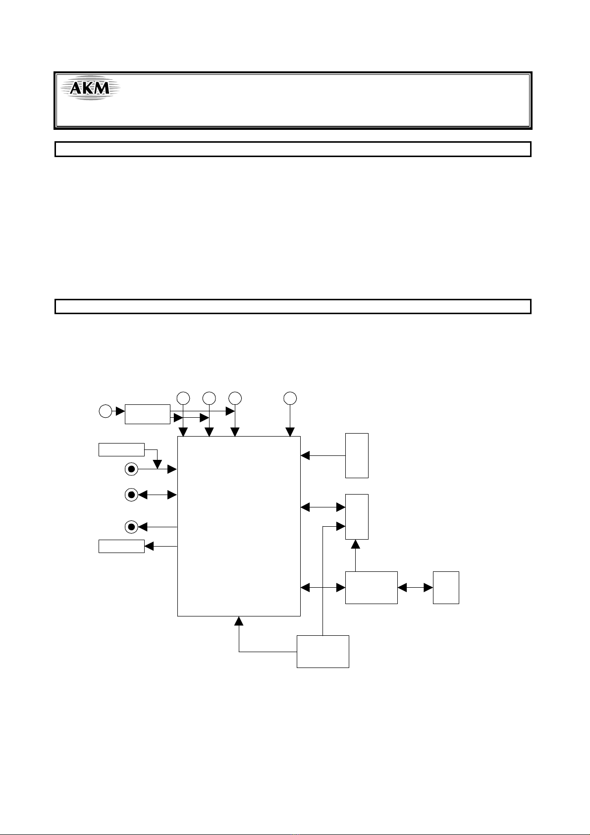
Evaluation Board Manual
Operation sequence
1) Set up the power supply lines.
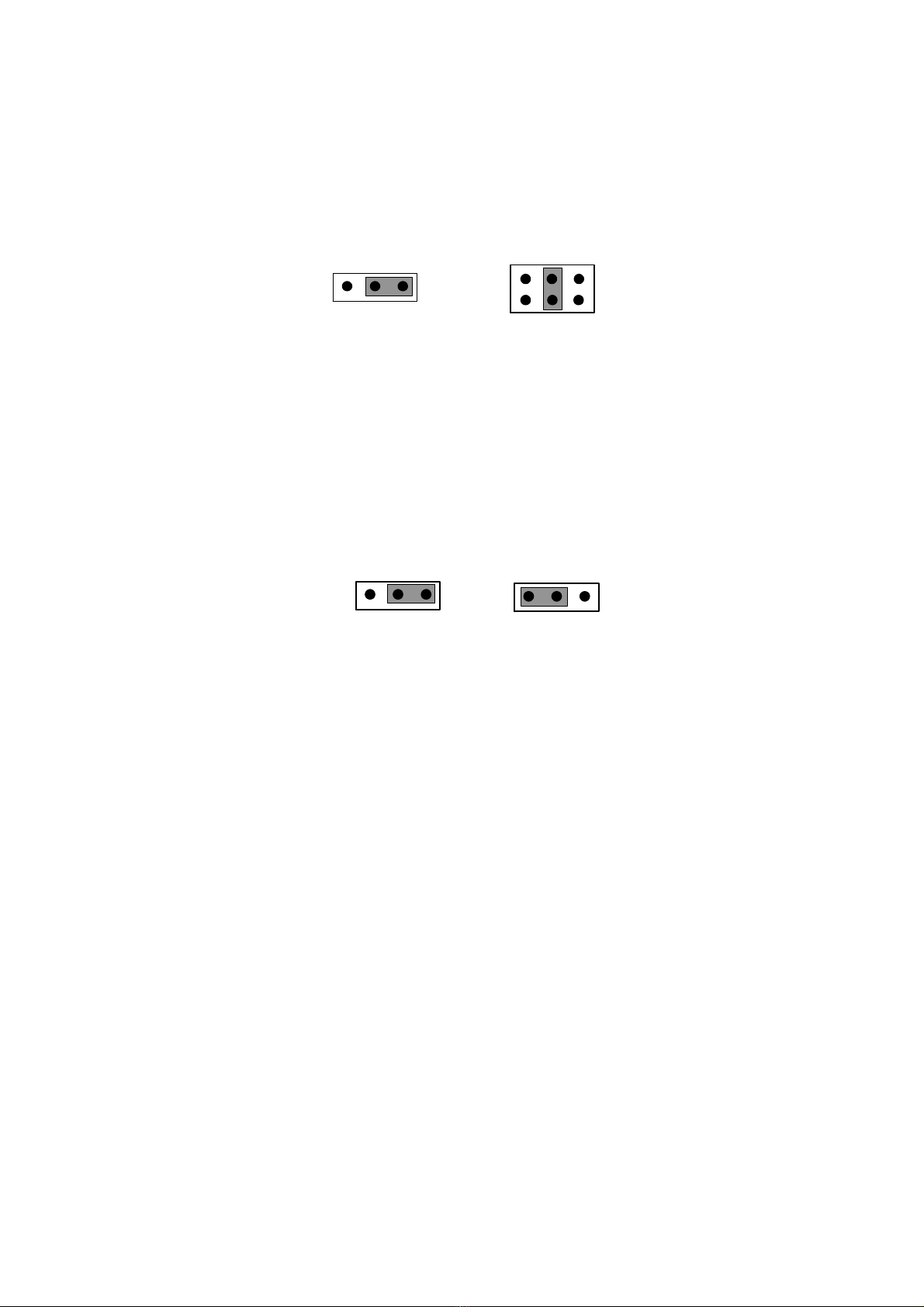
1-1) When AVDD,DVDD, SVDD, and VCCare supplied from the regulator. (AVDD, DVDD, SVDD, and VCC
jack should be open.). See “Other jumper pins set up (page 10)”. <default>
[REG] (red ) = 5V
[AVDD] (orange) = open : 3.3V is supplied to AVDD of AK4633VN from regulator.
[DVDD] (orange) = open : 3.3V is supplied to DVDD of AK4633VN from regulator.
[SVDD](blue) = open : 3.3V is supplied to SVDD of AK4633VN from regulator.
[VCC] (orenge) = open : 3.3V is supplied to logic block from regulator.
[AVSS] (black) = 0V : for analog ground
[AGND] (black) = 0V : for analog ground
[DGND] (black) = 0V : for logic ground
1-2) When AVDD, DVDD, SVDD, and VCC are not supplied from the regulator. (AVDD, DVDD, SVDD, and
VCC jack should be junction.) See “Other jumper pins set up (page 10)”.
[REG] (red) = “REG” jack should be open.
[AVDD] (orange) = 2.6 3.6V : for AVDD of AK4633VN (typ. 3.3V)
[DVDD] (orange) = 2.6 3.6V : for DVDD of AK4633VN (typ. 3.3V)
[SVDD] (blue) = 2.6 5.25V: for SVDD of AK4633VN (typ. 3.3V, 5.0V)
[VCC] (orenge) = 2.6 3.6V : for logic (typ. 3.3V)
[AVSS] (black) = 0V : for analog ground
[AGND] (black) = 0V : for analog ground
[DGND] (black) = 0V : for logic ground
Each supply line should be distributed from the power supply unit.
AVDD and DVDD must be same voltage level.
2) Set up the evaluation mode, jumper pins and DIP switches. (See the followings.)
3) Power on.
The AK4633VN and AK4114 should be reset once bringing SW1, 2 “L” upon power-up.
Evaluation mode
In case of AK4633VN evaluation using AK4114, it is necessary to correspond to audio interface format for
AK4633VN and AK4114. About AK4633VN’s audio interface format, refer to datasheet of AK4633VN.
About AK4114’s audio interface format, refer to Table 2 in this manual.
Applicable Evaluation Mode
(1) Evaluation of loop-back mode (A/D D/A) : PLL, Master Mode
(2) Evaluation of loop-back mode (A/D D/A) : PLL, Slave Mode (PLL Reference CLOCK: MCKI
pin)
(3) Evaluation of loop-back mode (A/D D/A) : PLL, Slave Mode (PLL Reference CLOCK: BICK or
FCK pin)
(4) Evaluation of using DIR of AK4114 (opt-connector) : EXT, Slave Mode
(5) Evaluation of using DIT of AK4114 (opt-connector) : EXT, Slave Mode
ASAHI KASEI [AKD4633-A]
<KM079407> 2016/10
- 3 -
(1) Evaluation of loop-back mode (A/D D/A) : PLL, Master Mode
a) Set up jumper pins of MCKI clock
X’tal of 11.2896MHz, 12MHz, 12.288MHz, 13MHz, 24MHz or 27MHz can be set in X2. X’tal of 12.288MHz
(Default) is set on the AKD4633VN. Set “No.8 of SW3” to “H”.
When an external clock (11.2896MHz, 12MHz, 12.288MHz, 13MHz, 24MHz or 27MHz) through a RCA
connector (J8: EXT/BICK) is supplied, select EXT on JP21 (MCLK_SEL) and short JP17 (XTE). JP23 (EXT1)
and R26 should be properly selected in order to much the output impedance of the clock generator.
b) Set up jumper pins of BICK clock
Output frequency (16fs/32fs/64fs) of BICK should be set by “BCKO1-0 bit” in the AK4633VN.
There is no necessity for set up JP19.
c) Set up jumper pins of FCK clock
d) Set up jumper pins of DATA
When the AK4633VN is evaluated by loop-back mode (A/D D/A), the jumper pins should be set to the
following.
JP17
XTE MCLK_SEL
JP21 JP18
MKFS
256fs 512fs1024fs
XTL DIR EXT MCKO
JP6
MCKI
JP22
FCK_SEL
2fs EXT
JP28
FCK
ADCDIR
1fs
JP26
4631_SDTI
ADC
DAC/LOOP
JP30
SDTI
DIR ADC
JP29
JP20
BICK JP27 BICK_INV
THRINV DIR ADC
BICK
THRINV
BICK_SEL
JP19
EXT
16fs
32fs
64fs
ASAHI KASEI [AKD4633-A]
<KM079407> 2016/10
- 4 -
(2) Evaluation of loop-back mode (A/D D/A) : PLL, Slave Mode (PLL Reference CLOCK: MCKI pin)
a) Set up jumper pins of MCKI clock
X’tal of 12.288MHz (Default) is set on the AKD4633-A. In this case, the AK4633VN corresponds to PLL
reference clock of 12.288MHz. In this evaluation mode, the output clock from MCKO-pin of the AK4633VN is
supplied to a divider (U3: 74VHC4040), BICK and FCK clocks are generated by the divider. Then “MCKO bit”
in the AK4633VN should be set to “1”. When an external clock through a RCA connector (J8: EXT/BICK) is
supplied, select EXT on JP21 (MCLK_SEL) and short JP17 (XTE). JP23 (EXT1) and R26 should be properly
selected in order to match the output impedance of the clock generator.
b) Set up jumper pins of BICK clock
c) Set up jumper pins of FCK clock
d) Set up jumper pins of DATA
When the AK4633VN is evaluated by loop-back mode (A/D D/A), the jumper pins should be set to the
following.
JP17
XTE MCLK_SEL
JP21 JP18
MKFS
256fs 512fs1024fs
XTL DIR EXT MCKO
JP6
MCKI
JP28
FCK
ADCDIR
JP22
FCK_SEL
2fs EXT1fs
JP26
4631_SDTI
ADC
DAC/LOOP
JP30
SDTI
DIR ADC
JP29
JP20
BICK JP27 BICK_INV
THRINV DIR ADC
BICK
THRINV
BICK_SEL
JP19
EXT
16fs
32fs
64fs
ASAHI KASEI [AKD4633-A]
<KM079407> 2016/10
- 5 -
(3) Evaluation of loop-back mode (A/D D/A) : PLL, Slave Mode (PLL Reference CLOCK: BICK or FCK
pin)
a) Set up jumper pins of BICK clock
When an external clock through a RCA connector J8 (EXT/BICK) is supplied, select EXT on JP19
(MCLK_SEL) and short JP17 (XTE). JP23 (EXT1) and R26 should be properly selected in order to match the
output impedance of the clock generator.
In this evaluation mode, the selected clock from JP21 (MCLK_SEL) is supplied to a divider (U3: 74VHC4040),
BICK and FCK clocks are generated by the divider. Input frequency of master clock is set up in turn “256fs”,
“512fs”, “1024fs” from left.
And input frequency of BICK is set up in turn “16fs”, “32fs”, “64fs” from left.
JP17
XTE MCLK_SEL
JP21
XTL DIR EXT
JP29
JP20
BICK JP27 BICK_INV
THRINV DIR ADC
BICK
THRINV
JP18
MKFS
256fs 512fs1024fsMCKO
JP18
MKFS
256fs 512fs1024fsMCKO
JP18
MKFS
256fs 512fs1024fsMCKO
BICK_SEL
JP19
EXT16fs32fs64fs
BICK_SEL
JP19
EXT16fs32fs64fs
BICK_SEL
JP19
EXT16fs32fs64fs
ASAHI KASEI [AKD4633-A]
<KM079407> 2016/10
- 6 -
b) Set up jumper pins of FCK clock
When an external clock through a RCA connector J9 (FCK) is supplied, select EXT on JP22 (FCK_SEL). JP24
(EXT2) and R27 should be properly selected in order to match the output impedance of the clock generator.
c) Set up jumper pins of DATA
When the AK4633VN is evaluated by loop-back mode (A/D D/A), the jumper pins should be set to the
following.
JP28
FCK
ADCDIR
JP22
FCK_SEL
2fs EXT1fs
JP26
4633_SDTI
ADC
DAC/LOOP
JP30
SDTI
DIR ADC
ASAHI KASEI [AKD4633-A]
<KM079407> 2016/10
- 7 -
(4) Evaluation of using DIR of AK4114 (opt-connector) : EXT, Slave Mode
a) Set up jumper pins of MCKI clock
b) Set up jumper pins of BICK clock
c) Set up jumper pins of FCK clock
JP24 (EXT2) and R27 should be properly selected in order to match the output impedance of the clock generator.
d) Set up jumper pins of DATA
When D/A converter of the AK4633VN is evaluated by using DIR of AK4114, the jumper pins should be set to
the following.
JP17
XTE MCLK_SEL
JP21
XTL DIR EXT
JP6
MCKI JP18
MKFS
256fs 512fs1024fs
JP29
JP20
BICK JP27 BICK_INV
THRINV DIR ADC
BICK
THRINV
BICK_SEL
JP19
EXT
16fs32fs
64fs
JP28
FCK
ADCDIR
JP22
FCK_SEL
2fs EXT1fs
JP26
4633_SDTI
ADC
DAC/LOOP
JP30
SDTI
DIR ADC
ASAHI KASEI [AKD4633-A]
<KM079407> 2016/10
- 8 -
(5) Evaluation of using DIT of AK4114 (opt-connector) : EXT, Slave Mode
a) Set up jumper pins of MCKI clock
b) Set up jumper pins of BICK clock
c) Set up jumper pins of FCK clock
JP24 (EXT2) and R27 should be properly selected in order to match the output impedance of the clock generator.
d) Set up jumper pins of DATA
When A/D converter of the AK4633VN is evaluated by using DIR of AK4114, the jumper pins should be set to
the following.
JP17
XTE MCLK_SEL
JP21
XTL DIR EXT
JP6
MCKI JP18
MKFS
256fs 512fs1024fs
JP28
FCK
ADCDIR
JP22
FCK_SEL
2fs EXT1fs
JP26
4633_SDTI
ADC
DAC/LOOP
JP30
SDTI
DIR ADC
JP29
JP20
BICK JP27 BICK_INV
THRINV DIR ADC
BICK
THRINV
BICK_SEL
JP19
EXT
16fs32fs
64fs
ASAHI KASEI [AKD4633-A]
<KM079407> 2016/10
- 9 -
DIP Switch set up
[SW3] (MODE) : Mode Setting of AK4633-VN and AK4114
ON is “H”, OFF is “L”.
No. Name ON (“H”) OFF (“L”)
1 DIF0 AK4114 Audio Format Setting
See Table 2
2 DIF1
3 DIF2
4 CM0 Clock Operation Mode select
See Table 3
5 CM1
6 OCKS0 Master Clock Frequency Select
See Table 4
7 OCKS1
8 M/S Master mode Slave mode
Note. When the AK4633VN is evaluated Master mode, “No.8 of SW3” is set to “H”.
Table 1. Mode Setting for AK4633VN and AK4114
Resistor setting
for AK4633VN Audio
Interface Format Setting for AK4114 Audio Interface Format
DIF1 bit DIF0 bit DIF0 DIF1 DIF2 DAUX SDTO
0 1 L L L 24bit, Left justified 16bit, Right justified
1 0 L L H 24bit, Left justified 24bit, Left justified Default
1 1 H L H 24bit, I2S 24bit, I2S
Note. When the AK4633VN is evaluated by using DIR/DIT of AK4114, “No.8 of SW3” is set to “L”.
Table 2. Setting for AK4114 Audio Interface Format
Mode CM1 CM0 UNLOCK PLL X'tal Clock source SDTO
0 0 0 - ON ON(Note) PLL RX
1 0 1 - OFF ON X'tal DAUX
2 1 0 0 ON ON PLL RX Default
1 ON ON X'tal DAUX
3 1 1 - ON ON X'tal DAUX
ON: Oscillation (Power-up), OFF: STOP (Power-down)
Note : When the X’tal is not used as clock comparison for fs detection (i.e. XTL1,0= “1,1”), the X’tal is off.
Default setting is recommended.
Table 3. Clock Operation Mode select
No. OCKS1 MCKO1 MCKO2 X’tal Default
0 0 256fs 256fs 256fs
2 1 512fs 256fs 512fs
Table 4. Master Clock Frequency Select (Stereo mode)
ASAHI KASEI [AKD4633-A]
<KM079407> 2016/10
- 10 -
Other jumper pins set up
1. JP1 (GND) : Analog ground and Digital ground
OPEN : Separated.
SHORT : Common. (The connector “DGND” can be open.) <Default>
2. JP2 (MICP) : Connection between MICP pin and BEEP pin of the AK4633VN.
MICP : MIC Differential input.
BEEP : BEEP input. <Default>
3. JP3 (AVDD_SEL) : AVDD of the AK4633VN
REG : AVDD is supplied from the regulator (“AVDD” jack should be open). < Default >
AVDD : AVDD is supplied from “AVDD ” jack.
4. JP9 (DVDD_SEL) : DVDD of the AK4633VN
AVDD : DVDD is supplied from “AVDD”. < Default >
DVDD : DVDD is supplied from “DVDD ” jack.
5. JP10 (LVC_SEL) : Logic block of LVC is selected supply line.
DVDD : Logic block of LVC is supplied from “DVDD”. < Default >
VCC : Logic block of LVC is supplied from “VCC ” jack.
6. JP11 (VCC_SEL) : Logic block is selected supply line.
LVC : Logic is supplied from supply line of LVC. < Default >
VCC : Logic block of LVC is supplied from “VCC ” jack.
7. JP4 (SVDD_SEL) : SVDD of the AK4633VN
REG : SVDD is supplied from the regulator (“SVDD” jack should be open). < Default >
SVDD : SVDD is supplied from “SVDD ” jack.
8. JP8 (MCKO_SEL) : Master Clock Frequency is selected clock from MCKO1 or MCKO2 of the AK4114.
MCKO1 : The check from MCKO1 of AK4114 is provided to MCKI of the AK4633VN. < Default >
MCKO2 : The check from MCKO2 of AK4114 is provided to MCKI of the AK4633VN.