[AKD4133-A]
< KM119500> 2016/11
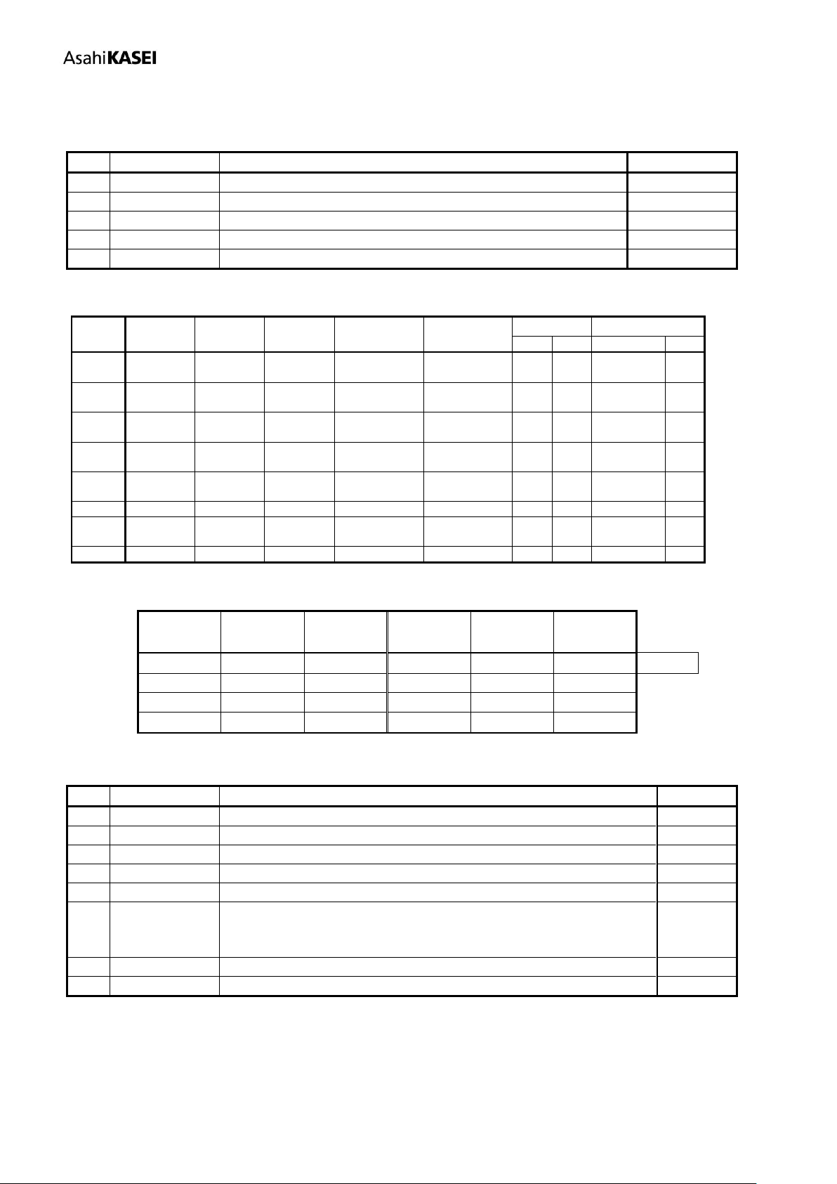
Board Diagram
Figure 2. AKD4133-A Board Diagram
Description
(1) U100 ( AK4133 )
2channels input/output Digital Sample Rate Converter (SRC).
(2) J200, J300 ( BNC Connector for Digital Input/Output )
J200 BNC connector : Digital Input optical signal to AK4118A(U200).
J300 BNC connector : Digital Output optical signal from AK4118A(U300).
(3) PORT200, PORT300 ( Optical Connector )
PORT200 : Digital Input optical signal to AK4118A(U200).
PORT300 : Digital Output optical signal from AK4118A(U300).
(4) J600, J601, J602, J603, J604 ( Power supply )
J600 (DVSS) : GND
J601 (+5V) : +5V Power Supply
J602 (DVDD) : + 3.3V/+1.8V Power Supply
J603 (VDD18) : +1.8V Power Supply
J604 (D33V) : +3.3V Power Supply
(5) U200, U300 ( AK4118A )
AK4118A has DIR, DIT and X’tal oscillator.
Transports input data to AK4133 when working in master mode, and output data from AK4133
when working in slave mode.
(6) J400 (BNC Connector)
Input external clock source.
(7) SW200, SW300 ( Dip-switch )
DIP type switch. Sets clock and audio format of AK4118A.
DIF[2 : 0] used to set audio interface format and OCKS[1 : 0] used to master clock frequency.
(8) SW500 ( Dip-switch )
DIP type switch. Sets clock and audio format and filter of AK4133.