ASAHI KASEI [AKD5356]
<KM068501>2002/10
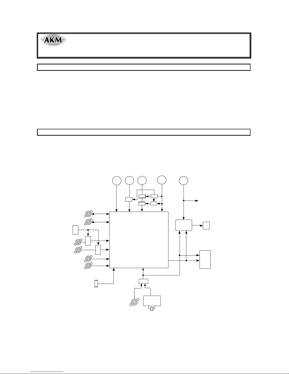
-10 -
2. [Function2 Dialog] : Dialog to evaluate IPGA
This dialog corresponds to only addr=03H.
Address Box: Input register address in 2 figures of hexadecimal.
Start Data Box: Input start data in 2 figures of hexadecimal.
End Data Box: Input end data in 2 figures of hexadecimal.
Interval Box: Data is written to AK5356by this interval.
Step Box: Data changes by this step.
Mode Select Box:
If you check this check box, data reaches end data, and returns to start data.
[Example] Start Data = 00, End Data = 09
Data flow: 00 01 02 03 04 05 06 07 08 09 09 08 07 06 05 04 03 02 01 00
If you do not check this check box, data reaches end data, but does not return to start data.
[Example] Start Data = 00, End Data = 09
Data flow: 00 01 02 03 04 05 06 07 08 09
If you want to write the input data to AK5356, click “OK”button. If not, click “Cancel”button.
3. [Write Dialog] : Dialog to write data by mouse operation
There are dialogs corresponding to each register.
Click the “Write”button corresponding to each register to set up the dialog. If you check the check box, data becomes
“H”or “1”. If not, “L”or “0”.
If you want to write the input data to AK5356, click “OK”button. If not, click “Cancel”button.
nIndication of data
Input data is indicated on the register map. Red letter indicates “H”or “1”and blue one indicates “L”or “0”. Blank is the
part that is not defined in the datasheet.
nAttention on the operation
If you set up Function1 or Function2 dialog, input data to all boxes. Attention dialog is indicated if you input data or
address that is not specified in the datasheet or you click “OK”button before you input data. In that case set up the dialog
and input data once more again. These operations does not need if you click “Cancel”button or check the check box.