AKM AKD4637-B User manual

[AKD4637-B]
<KM120603> 2018/10
- 1 -
GENERAL DESCRIPTION
The AKD4637-B is an evaluation board for the AK4637 24bit CODEC with built-in PLL and MIC/SPK Amplifier.
The AKD4637-B has the interface with AKM’s A/D evaluation boards. Therefore, it’s easy to evaluate the
AK4637. The AKD4637-B also has the digital audio interface and can achieve the interface with digital audio
systems via opt-connector.
Ordering Guide
AKD4637-B --- Evaluation board for AK4637
(Control software is included in this package.)
FUNCTION
•Compatible with 2 types of interface
- Direct interface with AKM’s A/D converter evaluation boards
- DIT/DIR with optical input/output
•USB port for board control
Mini
Jack
Digital
MIC
REG
3.3V
SPK
SPP SPN
LINE-
OUT
Jack
AK4637
Opt In
PIC4550
AK4118A
(DIT/DIR)
External
Clock
AIN/IN+
/DMDAT
1.8V
REG
0V
5V
GND1
REG1
DMCK
DMDT
BEEP/IN-
/DMCLK
BEEP
J1
J2
Opt Out
USB
Port
LDO
(T3)
PORT1
PORT2
PORT3
TVDD
DVDD
AVDD
Figure 1. AKD4637-B Block Diagram
* Circuit diagram and PCB layout are attached at the end of this manual.
Evaluation board Rev.2 for AK4637
AKD4637-B

[AKD4637-B]
<KM120603> 2018/10
- 2 -
Operation Sequence
(1) Set up the power supply lines.
(1-1) In case of using the power supply connectors. <Default>
JP13
AVDDSEL
JP11
USB5V
5V
3.3V
(1-2) In case of supplying the power from regulator.
JP13
AVDDSEL
JP11
USB5V
5V
3.3V
Name of
Jack
Color
Default Setting
Using
REG1
red
5V
for regulator input
GND1
black
0V
ground
Table 1. Set up of power supply lines
(2) Set up the evaluation mode, jumper pins and DIP switch. (See the followings.)
(3) Power on.
The control software must be opened after the power supplies are applied.

[AKD4637-B]
<KM120603> 2018/10
- 3 -
Evaluation mode
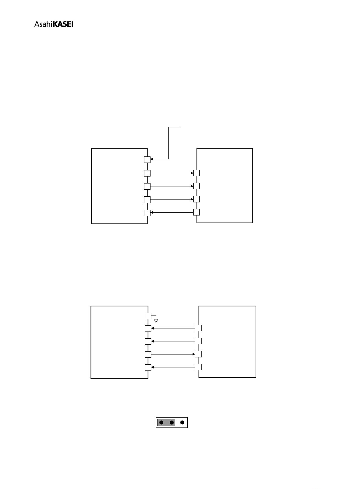
In case of using the AK4118A when evaluating the AK4637, audio interface format of both devices must be matched.
Refer to the datasheet for audio interface format of the AK4637, and Table 2 for audio interface format of the
AK4118A.
The AK4118A operates at fs of 32kHz or more. If the fs is slower than 32kHz, please use other mode.
In addition, MCLK of AK4118A supports 256fs and 512fs. When evaluating in a condition except above, please use
other mode.
Refer to the datasheet for register setting of the AK4637.
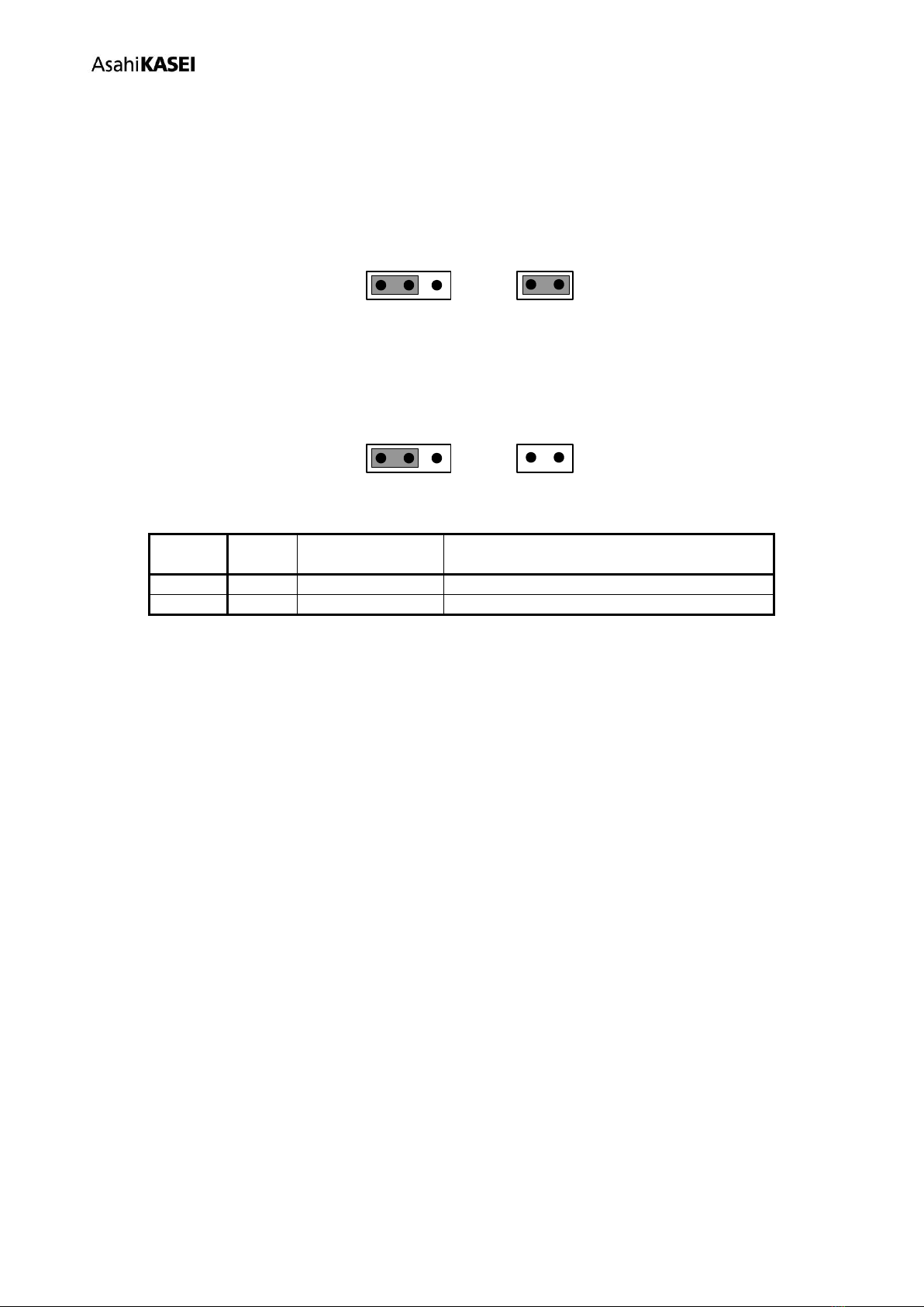
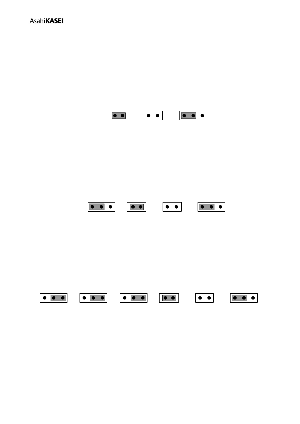
Applicable Evaluation Mode
(1) A/D Evaluation using the AK4118A (DIT).
(1-1) Setting in External Slave Mode
(2) D/A Evaluation using the AK4118A (DIR). <Default>
(2-1) Setting in External Slave Mode
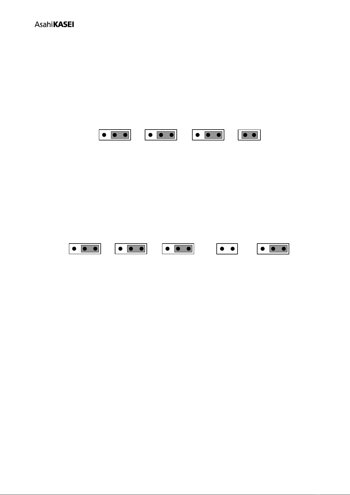
(3) Evaluation of A/D or D/A using the external clock.
(3-1) Setting in PLL Master Mode
(3-2) Setting in PLL Slave Mode
(3-3) Setting in External Slave Mode
(4) Evaluation of Loop-back.
(4-1) Setting in PLL Master Mode
(4-2) Setting in PLL Slave Mode
(4-3) Setting in External Slave Mode

[AKD4637-B]
<KM120603> 2018/10
- 4 -
(1) A/D Evaluation using the AK4118A (DIT)
(1-1) Setting in External Slave Mode
X1 (X’tal: 12.288MHz) and PORT2 (DIT) are used. Do not connect anything to PORT1 (DIR).
Registers of the AK4637 should be set to “EXT Slave Mode”. MCKI, BICK and FCK are supplied from the
AK4118A, and SDTO of the AK4637 is output to the AK4118A.
The jumper pins should be set as follows.
JP5
MCKI
JP6
BICK
JP7
FCK
DIR
EXT
DIR
EXT
JP8
DIR
EXT
SDTO
(2) Evaluation of D/A using DIR of AK4118A. <Default>
(2-1) Setting in External Slave Mode
PORT1 (DIR) is used. Do not connect anything to PORT2 (DIT).
Registers of the AK4637 should be set to “EXT Slave Mode”.
The jumper pins should be set as follows.
JP5
MCKI
JP6
BICK
JP7
FCK
DIR
EXT
DIR
EXT
DIR
EXT
JP9
SDTI
DIR
ADC
JP10
SDTI-SEL

[AKD4637-B]
<KM120603> 2018/10
- 5 -
(3) A/D or D/A Evaluation using the external clock.
External clocks are used. Do not connect anything to PORT1 (DIR) and PORT2 (DIT).
(3-1) Setting in PLL Master Mode
The master clock is input from the MCKI pin of JP5. An internal PLL circuit generates BICK and FCK.
Registers of the AK4637 should be set to “PLL Master Mode”.
MCKI and SDTI are input into JP5 and JP9. FCK, BICK and SDTO are output from JP7, JP6 and JP8.
AK4637
DSP or P
BICK
FCK
SDTO
SDTI
BCLK
FCK
SDTI
SDTO
MCKI
1fs
16fs, 32fs, 64fs
11.2896MHz, 12MHz, 12.288MHz,
13.5MHz, 24MHz, 27MHz
Figure 2. PLL Master Mode
(3-2) Setting in PLL Slave Mode
A reference clock of PLL is selected among the input clocks that are supplied to the BICK pin. The required clock
to operate the AK4637 is generated by an internal PLL circuit.
Registers of the AK4637 should be set to “PLL Slave Mode”(Reference Clock = BICK).
BICK, FCK and SDTI are input into JP6, JP7 and JP9. SDTO is output from JP8.
AK4637
DSP or P
MCKI
BICK
FCK
SDTO
SDTI
BCLK
FCK
SDTI
SDTO
1fs
16fs, 32fs, 64fs
Figure 3. PLL Slave Mode 2(PLL Reference Clock: BICK pin)
The jumper pins should be set as follows.
JP5
MCKI
DIR
EXT

[AKD4637-B]
<KM120603> 2018/10
- 6 -
(3-3) Setting in External Slave Mode
Registers of the AK4637 should be set to “EXT Slave Mode”.
MCLK, BICK, FCK and SDTI are input into JP5, JP6, JP7 and JP9. SDTO is output from JP8.
AK4951EN
DSP or P
MCKI
BICK
LRCK
SDTO
SDTI
BCLK
LRCK
SDTI
SDTO
1fs
32fs
MCLK
256fs,384fs
512fs or 1024fs
Figure 4. EXT Slave Mode

[AKD4637-B]
<KM120603> 2018/10
- 7 -
(4) Evaluation in Loop-back Mode
(4-1) Setting in PLL Master Mode
Do not connect anything to PORT1 (DIR), PORT2 (DIT).
Registers of the AK4637 should be set to “PLL Master Mode”. MCLK should be supplied to JP5.
The jumper pins should be set as follows.
JP8
JP9
SDTO
SDTI
DIR
ADC
JP10
SDTI-SEL
(4-2) Setting in PLL Slave Mode
Do not connect anything to PORT1 (DIR) and PORT2 (DIT).
Registers of the AK4637 should be set to “PLL Slave Mode”(Reference Clock: BICK).
BICK and FCK should be supplied to JP6 and JP7.
The jumper pins should be set as follows.
JP5
MCKI
JP8
DIR
EXT
JP9
SDTO
SDTI
DIR
ADC
JP10
SDTI-SEL
(4-3) Setting in External Slave Mode
Do not connect anything to PORT1 (DIR), PORT2 (DIT).
Registers of the AK4637 should be set to “EXT Slave Mode”.
Use clocks from AK4118A. In case, use X1 (12.288MHz).
The jumper pins should be set as follows.
JP5
MCKI
JP6
BICK
JP7
FCK
DIR
EXT
DIR
EXT
JP8
DIR
EXT
JP9
SDTO
SDTI
DIR
ADC
JP10
SDTI-SEL

[AKD4637-B]
<KM120603> 2018/10
- 8 -
DIP Switch Setting
[S1] (SW DIP-4): Mode setting of the AK4118A.
No.
Name
ON (“H”)
OFF (“L”)
Default
1
OCKS1
AK4118A Master Clock Setting : See Table 4
L
2
DIF0
AK4118A Audio Format Setting
See Table 3
L
3
DIF1
L
4
DIF2
H
Table 2. Mode Setting of the AK4118A
Mode
DIF2
DIF1
DIF0
DAUX
SDTO
FCK
BICK
I/O
I/O
0
0
0
0
24bit, Left justified
16bit, Right justified
H/L
O
64fs
O
1
0
0
1
24bit, Left justified
18bit, Right justified
H/L
O
64fs
O
2
0
1
0
24bit, Left justified
20bit, Right justified
H/L
O
64fs
O
3
0
1
1
24bit, Left justified
24bit, Right justified
H/L
O
64fs
O
4
1
0
0
24bit, Left justified
H/L
O
64fs
O
Default
5
1
0
1
24bit, I2S
24bit, I2S
L/H
O
64fs
O
6
1
1
0
24bit, Left justified
H/L
I
64 -128fs
I
7
1
1
1
24bit, I2S
24bit, I2S
L/H
I
64 -128fs
I
Table 3. AK4118A Audio Interface Format Setting
OCKS1
MCKO1
X’tal
Default
0
256fs
256fs
1
512fs
512fs
Table 4. AK4118A Master Clock Setting
Tact SW Function
[SW1] (PDN): Resets AK4637 and AK4118A. When Tact switch is pushed, PDN is “L”.
Control Port
It is possible to control AKD4637-B via general USB port. Connect cable with the USB connection (PORT3) on the
board and PC.

[AKD4637-B]
<KM120603> 2018/10
- 9 -
Analog Input/Output Circuits
(1) Input Circuits
Figure 5. AIN, IN+/IN- Input Circuits
(1-1) AIN Input Circuit (Single-ended Input) <Default>
AIN is input to J1.
When the Mic Power is not used, JP2 should be set to open.
JP3
IN-
JP1
S/D
JP2
IN+
AIN
MPWR
(1-2) IN+/IN- Input Circuit (Differential input)
IN+ and IN- are input to J1.
When the Mic Power is not used, JP2 and JP3 should be set to open.
JP3
IN-
JP1
S/D
JP2
IN+
AIN
MPWR
(1-3) BEEP Input Circuit
BEEP is input to TP10.
Do not connect anything to J1.
(1-4) Digital Mic Input Circuit
DMCK is output from TP11 and DMDT is input to TP12.
Do not connect anything to J1.

[AKD4637-B]
<KM120603> 2018/10
- 10 -
(2) Output Circuits
Figure 6. AOUT, SPP/SPN Output Circuit
(2-1) SPP/SPN Output Circuit <Default>
SPP and SPN are output from TP3 and TP4.
JP4
AOUT
(2-2) Monaural Line Output Circuit
AOUT is output from J2.
JP4
AOUT
* AKM assumes no responsibility for the trouble when using the above circuit examples.

[AKD4637-B]
<KM120603> 2018/10
- 11 -
Control Software Manual
Evaluation Board and Control Software Settings
1. Set up the evaluation board as needed, according to the previous terms.
2. Connect the evaluation board and PC with a USB cable.
3. The USB control is recognized as HID (Human Interface Device) on the PC.
4. Double-click the icon “akd4637.exe”to open the control program. (Note 1)
When the screen does not display “AKDUSBIF-B”at bottom left, reconnect the PC and the USB cable, and push
the [Port Reset] button.
5. Begin evaluation by following the procedure below.
Figure 7. Window of Control Soft
Note 1. The AK4637 should be reset by the SW1 after the power supplies are applied.

[AKD4637-B]
<KM120603> 2018/10
- 12 -
Operation Overview
Function and Register map are controlled by this control software. These controls may be selected by the upper tabs.
Frequentlyused buttons, such as the register initializing button “Write Default”, are located outside of the switching tab
window.
1.[Port Reset]: Resets the connection to PC.
Click this button when connecting USB cable after the control software set up.
2.[Write Default]: Register Initialization.
When the device is reset by a hardware reset, use this button to initialize the registers.
3.[All Write]: Executes write commands for all registers displayed.
4.[All Read]: Executes read commands for all registers displayed.
5.[Save]: “Save Address of Register”dialog box pops up.
6.[Load]: Executes data write from a saved file.
7.[All Reg Write]: “All Reg Write” dialog box pops up.
8.[Sequence]: “Sequence” dialog box pops up.
9.[Sequence (File)]: “Sequence (File)” dialog box pops up.
10. [Read]: Reads current register settings and displays to the register area (on the right of the main window).
(Add: Address, R: AK4637 Read value, W: Last Write value (= Register Map))
This is different from [All Read] button as it does not reflect to the register map. It only displays register
values in hexadecimal numbers.

[AKD4637-B]
<KM120603> 2018/10
- 13 -
Tab Functions
(1) [Function] Tab: Function Control
Sequence operation and a setup of a register are executed with the function button arranged at the upper part, and each
button in a block diagram.
Figure 8. [Function] Window
Function block : Executes a sequential process shown on each button. (Refer to (1-(1-1))
Path and Each Setting block : Executes a setup of the path or functions. (Refer to (1-(1-2))
~ Explanation of the color of a pass line ~
Thick lines (blue, red, yellow, and sour orange) show that the paths are connected.
・thick line (blue): The path is connected and the power of block on this path is "OFF".
・thick line (red): The path is connected and the power of block on this path is "ON".
・thick line (yellow): The clock line is connected.
・thick line (sour orange): The clock line is connected and used.

[AKD4637-B]
<KM120603> 2018/10
- 14 -
(1-1) Function block
Figure 9. [Function] Block
A function button executes the sequence process shown on the each button and updates several registers.
These functions are mainly for path settings.
Function Name
Description
Input
Output
Path
Analog MIC
(Recording_MIC+18dB(ALC ON))
MIC Input
Recording
AMIC
SDTO
AMIC→ADC→Digi.Fil→SDTO
Digital MIC
(Recording_DigitalMIC(ALC ON))
Digital MIC
Input Recording
DMDAT
/DMCLK
SDTO
DMDAT/DMCLK→Deci.Fil→
Digi.Fil→SDTO
Speaker
(Playback_Speaker+8.4dB(ALC ON))
Speaker Output
SDTI
SPP/SPN
SDTI→Digi.Fil→DAC→
SPP/SPN
Line
(Playback_Lineout)
Line Output
SDTI
AOUT
SDTI→DAC→AOUT
AMIC-Line
(Loopback_MIC+18dB_LineOut
(ALC ON))
Loopback
(MIC Input,
Line Output)
AMIC,
AOUT
AMIC→ADC→Digi.Fil→DAC
→AOUT
Table 5. Sequence Process Setting
※The Setting of Clock mode and I/F mode are not changed. The default values are follows.
I/F mode: 24bit MSB justified

[AKD4637-B]
<KM120603> 2018/10
- 15 -
(1-1-1) [Analog MIC (Recording_MIC+18dB(ALC ON))] Sequential process
When [Analog MIC] button in the main window is clicked, the sequence for MIC input Settings is executed.
(Note 2)
Figure 10. [Analog MIC] Setting (After)
Note 2. The function button makes some block power up, but [Power Down/Up] button is not changed.

[AKD4637-B]
<KM120603> 2018/10
- 20 -
(1-2) Path and Various Setting Block
The enabled paths are shown. The FS and CM bits, etc… can be set up.
[Input_ADC Setting], [Digital Filter Setting], [ALC Setting], [DAC_Output Setting], [BEEP Setting] -- each
setting dialog can be opened.
Figure 15. [Path and Various Setting] Block
[Input_ADC Setting] button : Opens “Input_ADC”dialog box.
[Digital Filter Setting] button : Opens “Filter Setting”dialog box.
[ALC Setting] Button : Opens “ALC Setting”dialog box.
[DAC_Output Setting] button : Opens “DAC_Output Setting”dialog box.
This dialog also has a setup of Speaker amplifier and lineout amplifier.
[BEEP Setting] button : Opens “BEEP Setting”dialog box.
BEEP Power [OFF/ON] button : The path of a BEEP output is controlled and performs a BEEPS output
“OFF/ON.”
[ON]: BEEPS is set “1” and BEEPS bit Switch is connected. (Note 3)
BEEPS bit switch : This switch is interlocked with BEEPS bit.
DACS/L bit switch : This switch is interlocked with DACS bit and DACL bit. (Note 4)
[Power Down/Up] button : Using the present path setting, the path for recording is set and ON/OFF of
PMx bit is changed. (Note 3)
Note 3. There are some register bits which are set up automatically at Power Up/Down. (Refer to the next page.)
Note 4. The DACS (or DACL) switch on a GUI screen is updated by selection situation of a speaker/lineout.
When "LOSEL=0 and DACS=1" or "LOSEL=1 and DACL=1", the switch "is connected".
Other case, the switch "is disconnected".
Table of contents
Other AKM Motherboard manuals