ASAHI KASEI [AKD4127-A]
<KM085601> 2006/11
- 4 -
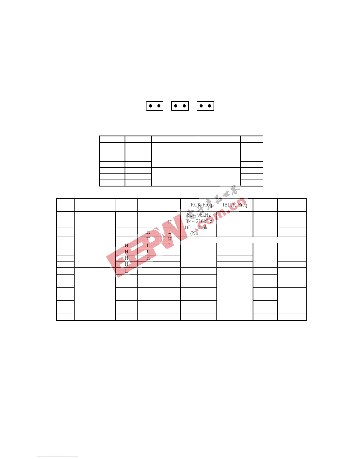
Mode IDIF2 IDIF1 IDIF0 SDTI Format ILRCK IBICK IBICK Freq Master / Slave
0 L L L 16bit, LSB justified ≥32fsi
1 L L H 20bit, LSB justified ≥40fsi
2 L H L 24/20bit, MSB justified ≥48fsi
3 L H H 24/16bit, I2S Compatible ≥48fsi or
32fsi
4 H L L 24bit, LSB justified
Input Input
≥48fsi
Slave
5 H L H 24bit, MSB justified 64fs
6 H H L 24bit, I2S Compatible Output Output 64fs Master
7 H H H Reserved
Table 4. Input Audio Interface Format (Input PORT)
(2) Setting for Output port
(1) When using DIT function of AK4114 (U4)
When using PORT4 (DIT) or J2 (TX), nothing should be connected to PORT3 (OUTPUT). When BICK and
LRCK frequencies are changed, the value of X’tal (X1) frequency should be changed.
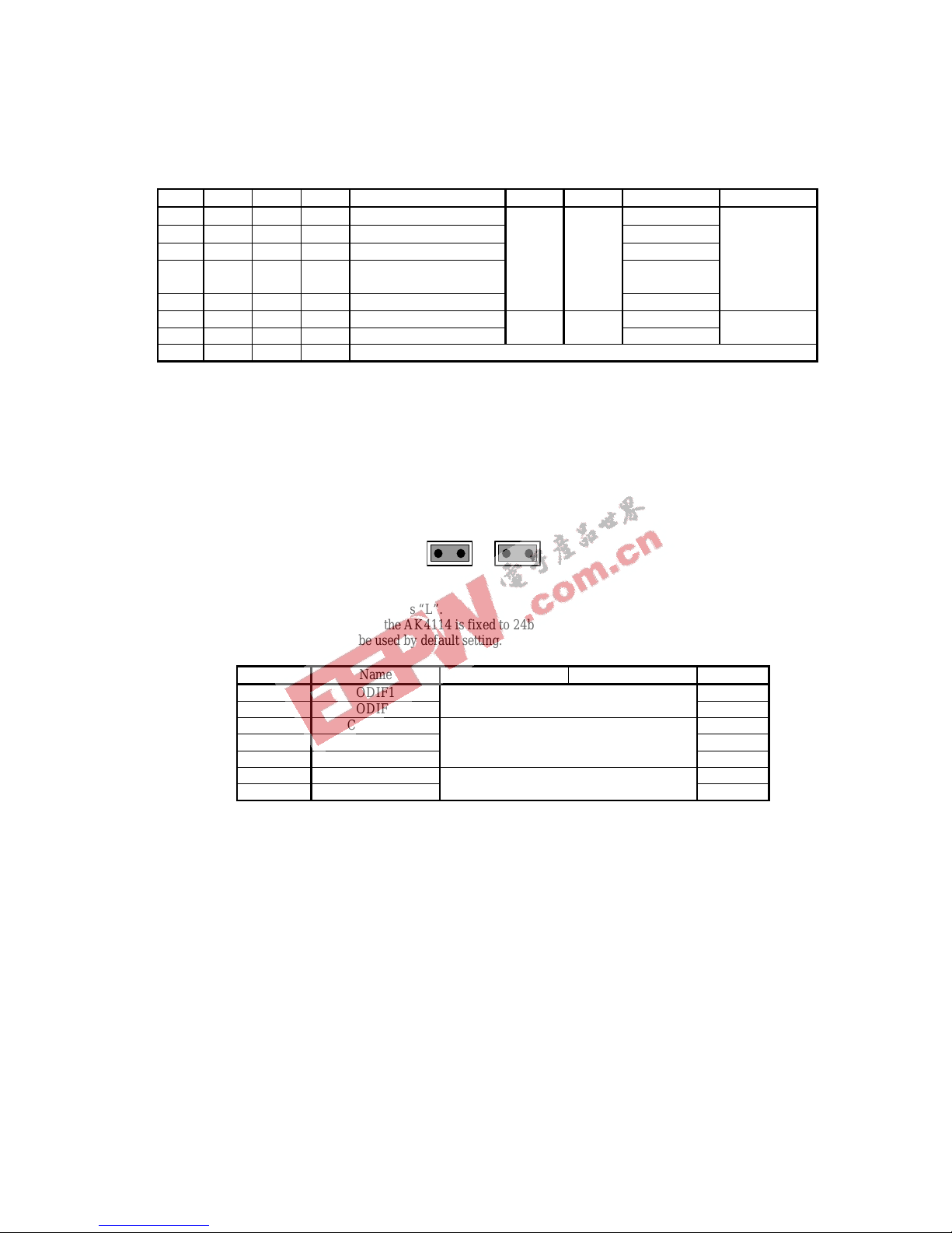
JP6
OBICK JP7
OLRCK
•SW4 setting (See Table 5)
Upper-side is “H” and lower-side is “L”.
The audio interface format of the AK4114 is fixed to 24bit, MSB justified. ODIF2-0, CMODE2-0 and
OBIT1-0 of SW3 should be used by default setting.
SW4 No. Name ON (“H”) OFF (“L”) Default
1 ODIF1 H
2 ODIF0
AK4127 Output Audio I/F Format Setting
Fixed to default L
3 CMODE2 H
4 CMODE1 L
5 CMODE0
AK4127 Mode Setting
Fixed to default L
6 OBIT1 H
7 OBIT0 AK4127 Output bit Length Setting
Fixed to default H
Table 5. SW4 Setting