[AKD4114-B]
[KM076604] 2009/08
- 4 -
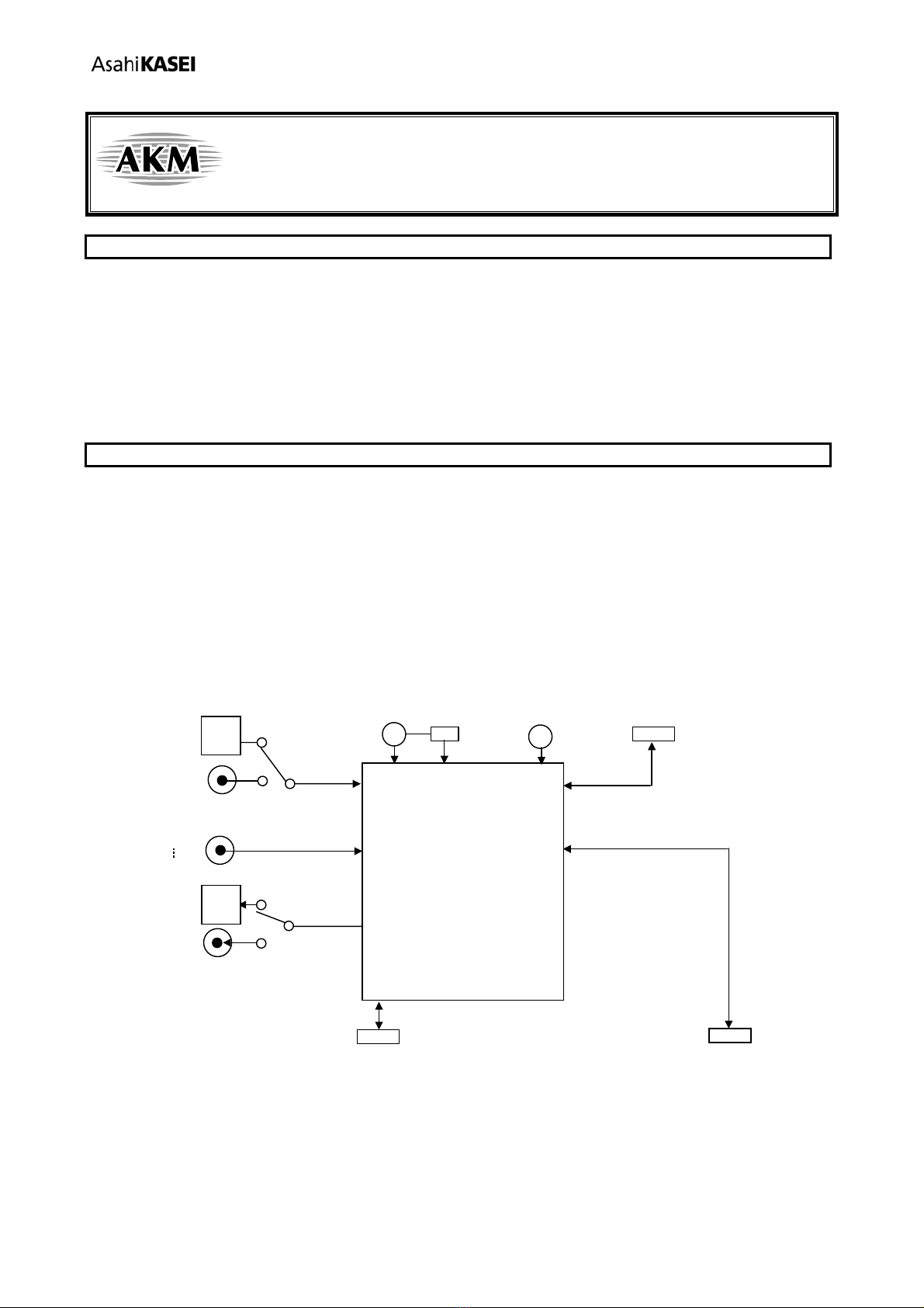
b-2. Set-up of input/output of BICK and LRCK
Please select SW 3_7 (DIR_I/O) according to the setup of audio format of AK4114 (Refer to Table 7).
Audio format SW3_7 (DIR_I/O)
Slave mode 0 Default
Master mode 1
Table 6. Set-up of DIR_I/O
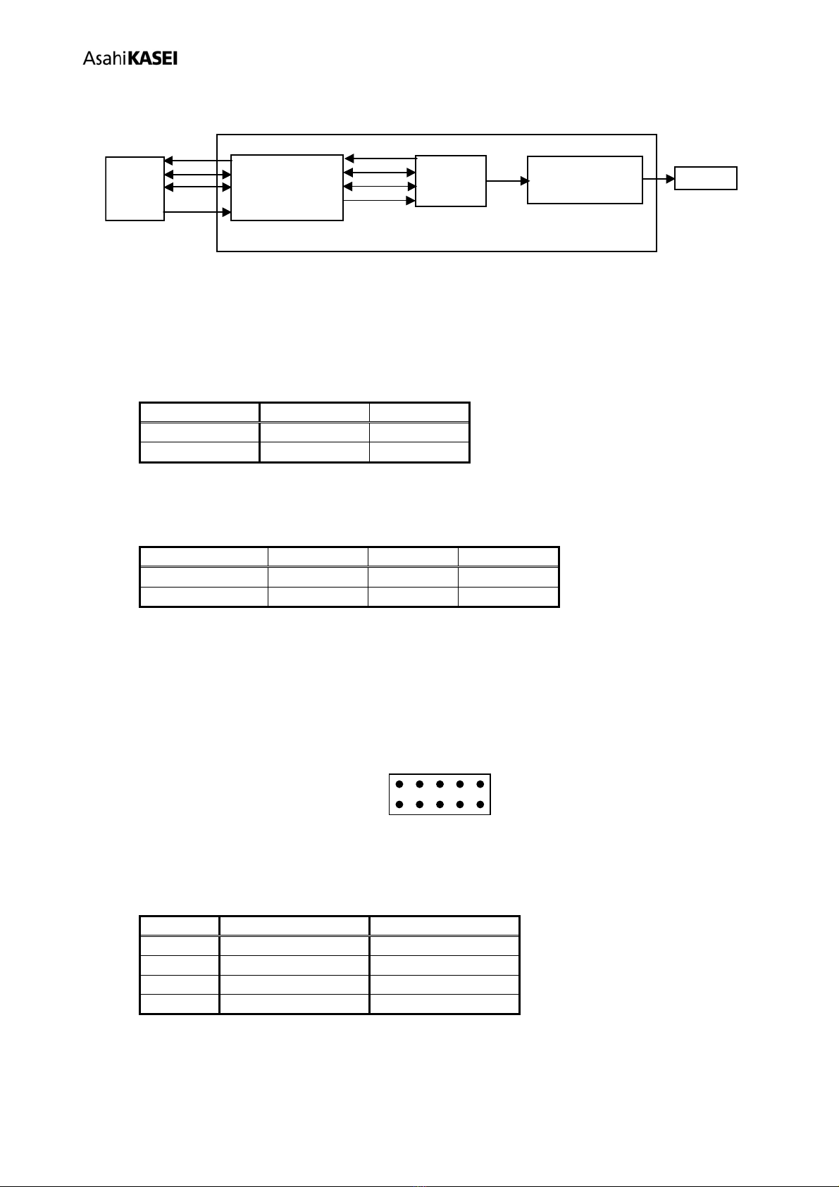
c. Set-up of Audio format
It sets up by SW 1_2, SW 1_3 and SW1_4 in parallel mode. Please set up DIF2-0 bit in serial mode.
DIF2 pin
(SW1_4)
DIF1 pin
(SW1_3)
DIF0 pin
(SW1_2) LRCK BICK
Mode
DIF2 bit DIF1 bit DIF0 bit
DAUX SDTO
I/O I/O
0 0 0 0
24bit, Left
justified
16bit, Right
justified H/L O 64fs O
1 0 0 1
24bit, Left
justified
18bit, Right
justified H/L O 64fs O
2 0 1 0
24bit, Left
justified
20bit, Right
justified H/L O 64fs O
3 0 1 1
24bit, Left
justified
24bit, Right
justified H/L O 64fs O
4 1 0 0
24bit, Left
justified
24bit, Left
justified H/L O 64fs O
5 1 0 1 24bit, I2S 24bit, I2S L/H O 64fs O
6 1 1 0
24bit, Left
justified
24bit, Left
justified H/L I 64-128fs I Default
7 1 1 1 24bit, I2S 24bit, I2S L/H I 64-128fs I
Table 7. Audio format
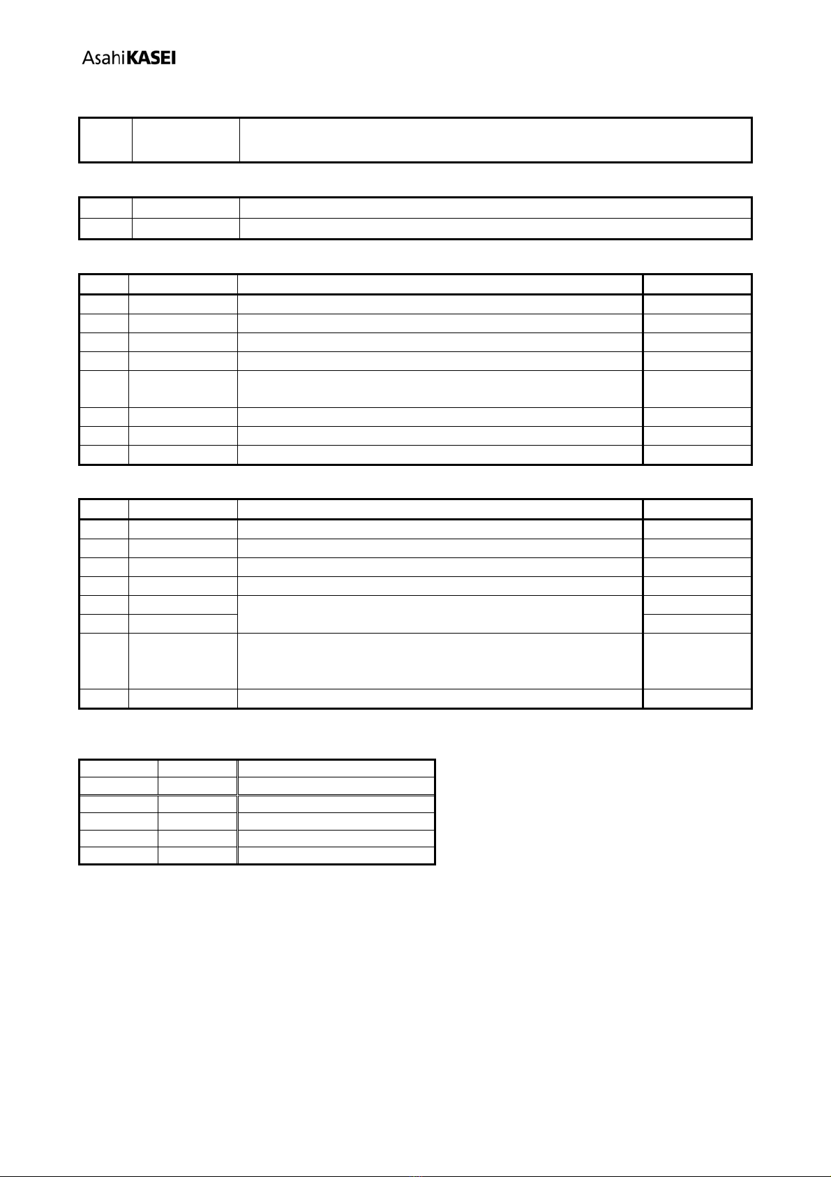
d. Set-up of CM1 and CM0
The operation mode of PLL is selected by CM1 and CM0. In parallel mode, it can be selected by SW3_1 and
JP18. In serial mode, it can be selected by CM1-0 bits.
CM1 pin
(SW3_1) CM0 pin (JP18)
CM1 bit CM0 bit
(UNLOCK) PLL X'tal Clock
source
SDTO
source
0 0 (CM0) - ON ON(Note) PLL(RX) RX
Default
0 1 (CDTO/CM0=H) - OFF ON X'tal DAUX
0 ON ON PLL(RX) RX
1 0 (CM0) 1 ON ON X'tal DAUX
1 1 (CDTO/CM0=H) - ON ON X'tal DAUX
ON: Oscillation (Power-up), OFF: STOP (Power-Down)
Note: When the X’tal is not used as clock comparison for fs detection (XTL0, 1= “1,1”), the X’tal is OFF.
Table 8. Clock Operation Mode Select