[AKD7736A-A]
<KM113102> 2012/12
- 6 -
(1) Digital-to-Digital Evaluation using ADC Port and DAC Port: CKM Master Mode = 0/1
ADC-Port and DAC-Port are used on this evaluation. Set the clock mode of the AK7736A to CKM Master Mode
0 (12.288MHz) or CKM Master Mode 1 (18.432MHz). The AK7736A outputs BICK and LRCK to the ADC-Port
and DAC-Port by setting the FPGA. The ADC-Port inputs data to the SDIN1, SDIN2A, SDIN2B, SDIN2C,
SDIN3 or SDIN4 pin. The DAC-Port output data from the SDOUT1, SDOUT2A, SDOUT2B, SDOUT3 or
SDOUT4 pin.
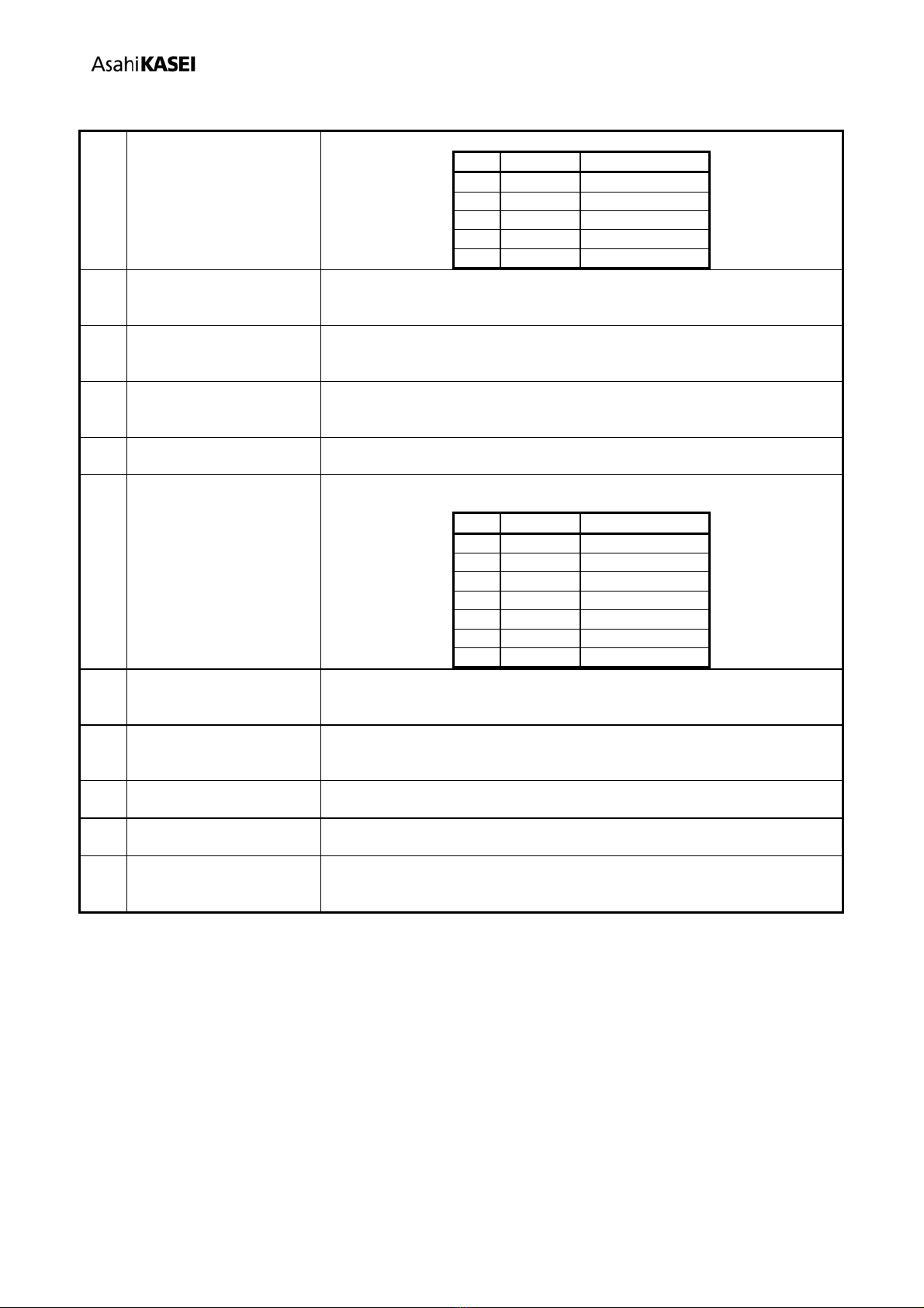
[Jumper Pins Setting]
JP1
XTI-SEL
CRYEXT
For digital output, optical connector PORT2 (SPDIF-OUT) is also available. The following setting must be made
and the FPGA setting should be changed when using the SPDIF-OUT instead of the DAC-Port. Refer to
“AK4118A Setting” for detail setting of the AK4118A.
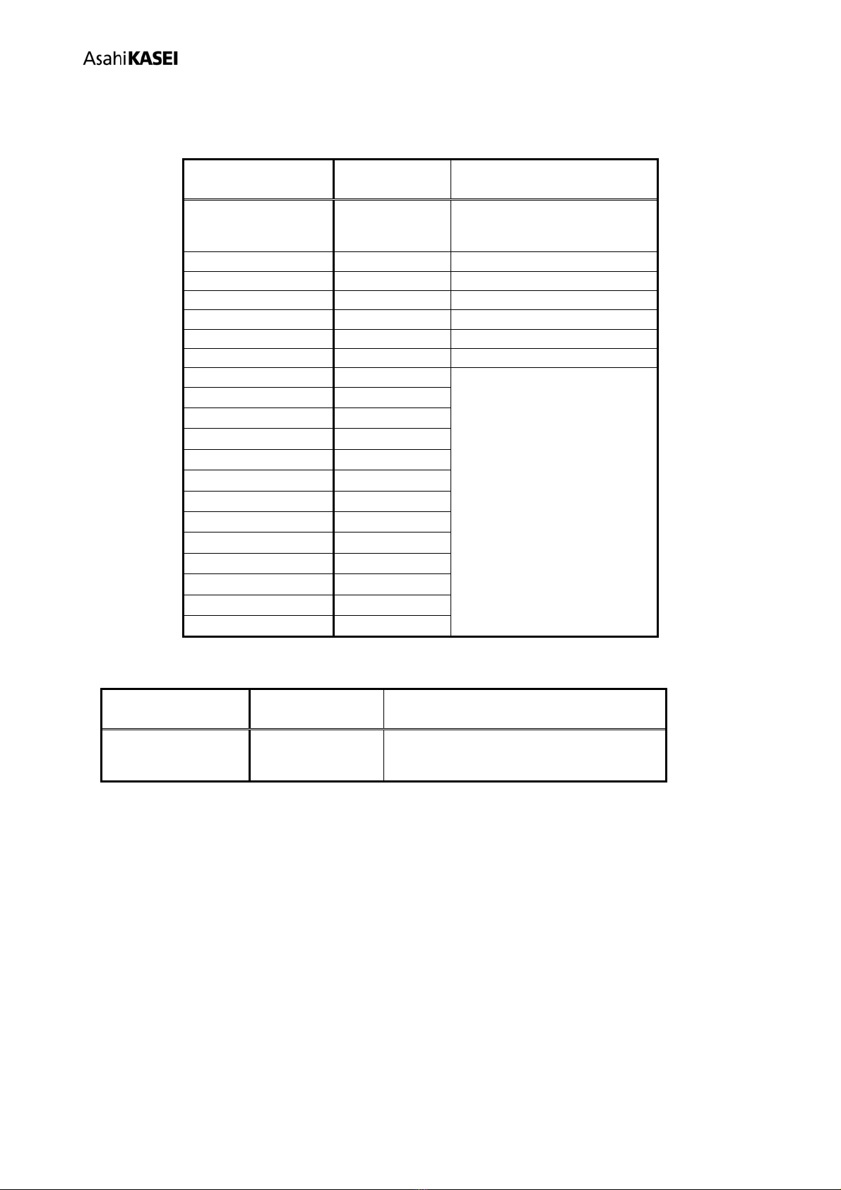
Main Board
Jumper / Switch Setting (Default)
SW1 (AK4118A
Clock) “TX-CLK”
S1(AK4118A Setting) 1->7=LHLLLHH
Table 3. Configuration of the AK4118A switch in Master Mode
(2) Digital-to-Digital Evaluation using ADC Port and DAC Port: CKM Slave Mode = 2/3/4/5
ADC-Port and DAC-Port are used on this evaluation. Set the clock mode of AK7736A to CKM Slave Mode
2/3/4/5. ADC-Port supplies MCLK, BICK, LRCK and digital data to the AK7736A. (MCLK is needed in CKM
Slave Mode 2 only)
[Jumper Pins Setting]
JP10
XTI-SEL
CRYEXT
(MCLK is needed in CKM Slave Mode 2 only)
For digital input and output, optical connector PORT1 (SPDIF-IN) and PORT2 (SPDIF-OUT) are available,
respectively. The following setting must be made and the FPGA setting should be changed when using these
connectors. Refer to “AK4118A Setting” for detail setting of the AK4118A.
Main Board
Jumper / Switch Setting (Default)
SW1 (AK4118A
Clock) “XTL”
S1(AK4118A Setting) 1->7=LHLLLLH
Table 4. Configure the AK4118A switch at the Slave Mode