manuals.online logo
Brands
  1. Home
  2. •
  3. Brands
  4. •
  5. Alinco
  6. •
  7. Radio
  8. •
  9. Alinco DJ-C1 User manual

Alinco DJ-C1 User manual

Other manuals for DJ-C1

1

This manual suits for next models

1

Other Alinco Radio manuals

Alinco DR-235 User manual

Alinco

Alinco DR-235 User manual

Alinco DR-130 User manual

Alinco

Alinco DR-130 User manual

Alinco DJ-596T User manual

Alinco

Alinco DJ-596T User manual

Alinco DR-138 User manual

Alinco

Alinco DR-138 User manual

Alinco DR-1200T User manual

Alinco

Alinco DR-1200T User manual

Alinco DX-R8T User manual

Alinco

Alinco DX-R8T User manual

Alinco DJ-446 User manual

Alinco

Alinco DJ-446 User manual

Alinco DR-135T MkII User manual

Alinco

Alinco DR-135T MkII User manual

Alinco 135T User manual

Alinco

Alinco 135T User manual

Alinco DJ-493 User manual

Alinco

Alinco DJ-493 User manual

Alinco DR-MD500 User manual

Alinco

Alinco DR-MD500 User manual

Alinco DR-M03R User manual

Alinco

Alinco DR-M03R User manual

Alinco DR-1200T User manual

Alinco

Alinco DR-1200T User manual

Alinco DR-570T User manual

Alinco

Alinco DR-570T User manual

Alinco DJ - C7 T User manual

Alinco

Alinco DJ - C7 T User manual

Alinco DJ-V446 User manual

Alinco

Alinco DJ-V446 User manual

Alinco DR-135 User manual

Alinco

Alinco DR-135 User manual

Alinco DJ-S17 E User manual

Alinco

Alinco DJ-S17 E User manual

Alinco DR-235 User manual

Alinco

Alinco DR-235 User manual

Alinco DR-635 User manual

Alinco

Alinco DR-635 User manual

Popular Radio manuals by other brands

Grundig G6 AVIATOR owner's manual

Grundig

Grundig G6 AVIATOR owner's manual

Makita DMR114 instruction manual

Makita

Makita DMR114 instruction manual

PURE Move R3 manual

PURE

PURE Move R3 manual

Motorola CP040 Detailed service manual

Motorola

Motorola CP040 Detailed service manual

Bosch GPB18V-5C Operating/safety instructions

Bosch

Bosch GPB18V-5C Operating/safety instructions

Ocean Digital WR-230 user manual

Ocean Digital

Ocean Digital WR-230 user manual

Realistic TRC-457 owner's manual

Realistic

Realistic TRC-457 owner's manual

Uniden AX 144 owner's manual

Uniden

Uniden AX 144 owner's manual

SIGNIFY EA2173 instruction manual

SIGNIFY

SIGNIFY EA2173 instruction manual

auna multimedia 10026443 user manual

auna multimedia

auna multimedia 10026443 user manual

GME TX680 instruction manual

GME

GME TX680 instruction manual

Motorola MTM5 00 Series Basic service manual

Motorola

Motorola MTM5 00 Series Basic service manual

Tivoli Audio ONE+ owner's manual

Tivoli Audio

Tivoli Audio ONE+ owner's manual

Sirius Satellite Radio SDVK1 installation guide

Sirius Satellite Radio

Sirius Satellite Radio SDVK1 installation guide

Sirius XM RAdio EDGE user guide

Sirius XM RAdio

Sirius XM RAdio EDGE user guide

Trevi XF 100 user guide

Trevi

Trevi XF 100 user guide

EisSound KBSound iSelect user manual

EisSound

EisSound KBSound iSelect user manual

Kirisun DM588-02 user manual

Kirisun

Kirisun DM588-02 user manual

manuals.online logo
manuals.online logoBrands
  • About & Mission
  • Contact us
  • Privacy Policy
  • Terms and Conditions

Copyright 2025 Manuals.Online. All Rights Reserved.

DJ-C1/C4 Service Manual
CONTENTS
+SPECIFICATIONS 2
+DJ-CI CIRCUIT DESCRIPTION 3
+DJ-C4 CIRCUIT DESCRIPTION 5
+SEMICONDUCTOR DATA 9
+EXPLODED VIEW 17
+PARTS LIST 19
+ADJUSTMENT 23
+PCBOARD VIEW 27
+CIRCUIT DIAGRAM 34
+BLOCK DIAGRAM (DJ-C1) 43
+BLOCK DIAGRAM (DJ-C4) 44
ALINCO INCORPORATED
TWIN 21 M.I.D. TOWER BUILDING 23F, 1-61, 2-CHOME,
SHIROMI CHUO-KU , OSAKA, 540-8580 JAPAN
Tel (81)6-6946-8150 fax (81)6-6946-8175
e-mail: [email protected]
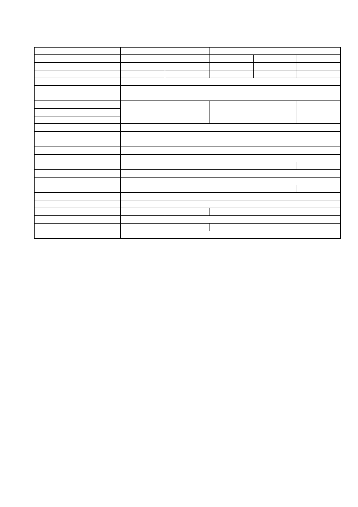
SPECIFICATIONS DJ-C1 DJ-C4
Version T E T E C
Receptionrange(MHz) 118.000~173.995 144.000~145.995 420.000~449.995 430.000~439.995 433.05~434.79
Transmission range (MHz) 144.000~147.995 144.000~145.995 420.000~449.995 430.000~439.995 433.05~434.79
Signal type F3E(FM)
Operating temperature Transceiver: -10~+50*C Charger:0-40oC
Rated voltage 3.7V
Power consumption Transmission : Approx.240mA Transmission : Approx.300mA Approx.180mA
Reception : Approx.30mA Reception : Approx.40mA Approx.40mA
(Rx squelched) (Rx squelched) (Rx squelched)
Ground Negative
Microphone input impedance Approx.2k ohm
Dimensions (Without projections) 94(H) x 56(W) x 10.6 (D)
Weight(With battery) 75g
Transmitter
Power output 300mW 10mW
Modulation system Reactance modulation
Max.frequency deviation +/- 5kHz
Spurious emission Max.-60dB Typ.-50dB
Receiver
Receiving system Double conversion superheterodyne
1stintermediate frequency 21.7MHz 20.8MHz 21.7MHz
2nd intermediate frequency 450kHz
Sensitivity Better than -16dBu Better than -15dBu
AF power output 20mW(32ohm)
Page 2
DJ-C1 CIRCUIT DESCRIPTION
1) Reception
1. Front End The signal picked up by the antenna is passed through a low-pass filter and
band-pass filter, and amplified by an RF amplifier (Q207). It is then passed
through another low-pass filter and sent to the mixer (Q209).
2. Mixer The mixer (Q209) creates the sum and difference of the received signal and
the first local signal The crystal filtter (XF201) selects the 21.7 MHz signal and
eliminates adjacent signals. The first IF amplifier (Q210) then amplifies the
selected signal. The upper side local signal is used as the first local signal It is
obtained by passing the signal from the VCO through two buffer amplifiers
(Q204 and Q208) and into the base of the mixer (Q209).
3.IF The signal amplified by the first IF amplifier (Q210) is input to pin 16 of the
demodulator circuit (IC207). A second local signal of 21 ,25 MHz is oscillated
by the crystal(X201) and IC202, and is input to pin 1 of the IC207. These two
signals are mixed by the demodulator's internal mixer and converted to a 450
kHz second IF signal. The converted second IF signal is output from pin 3 of
IC207 to a ceramic filter (FL201) where adjacent signals are eliminated. The
resulting signal is then sent back to pin 5 of IC207.
[FM]
The second IF signal input to pin 5 of IC207 is demodulated by the internal
limiter amplifier and quadrature detection circuit. It is then output as an audio
signal from pin 9.
[AM]
For AM, the S-meter output from pin 12 of IC207 is amplified by the AM audio
amplifier (Q220). Also, the AGC amplifier (Q221 ) forward-controls gain of the
first IF amplifier (Q210) in order that the correct audio signal is obtained even
when the input signal changes.
4. Squelch The squelch takes white noise from pin 9 of IC207 and inputs into pin 8 of
IC207. The noise passes through an internal noise filtter amplifier and rectifier
circuit, and is output from pin 14. The rectified voltage is input to the A/D port
of the microcomputer (IC101 ). The microcomputer turns audio output ON/OFF
based on this voltage:
Page-3
5. Audio Audio output is switched between AM and FM by IC209. Volume is controlled
by Q222 and Q223. The signal is input to pin 2 of the audio power amplifier
(IC208) and output from pin 6, thus producing sound from the earphones, etc.
6. VCO The VCO is built on a Colpits oscillator. Frequency is determined by D203,
D207 and L214, and the signal is oscillated by a transistor (Q203). The
oscillated signal is passed through a buffer amplifier (Q204) and input to pin 6
of a PLL circuit (IC204).
7. PLL Circuit The PLL circuit (IC204) is used to control the frequency oscillated by the VCO.
Control uses the serial control signal from the microcomputer (IC101). The
reference frequency that IC204 uses is oscillated to 21.25 MHz by IC202 in the
crystal oscillator (X201) and input to pin 1 of the IC204.
The IC204 divides the control signal sent to bin 6 from IC101 and the 21.25
MHz reference signal internally, and compares phases between the two. If a
difference is detected in the comparison, the charge pump in pin 9 outputs a
pulse signal. The pulse is converted to DC voltage by the PLL loop filter and
input to the cathode of the VCO varicaps (D203 and D207) in order to
eliminate the difference. This enables stable oscillation at the desired
frequency.
2) Transmission
1. Microphone Amplifier
The microphone amplifier (IC205) has two operating amplifiers. Sound is
converted to an electric signal and input to IC205. The input signal is amplified
for pre-emphasis and then output. The output signal is regulated for maximum
frequency deviation by VR202 and input to the cathode of the modulation
varicap (D206) of the VCO, thereby generating an FM signal by capicitance
change.
2. Power Amplifier The signal oscillated by the VCO is passed through two buffer amplifiers
(Q204 and Q218) and an exciter (Q206), and is then input to a power amplifier
(Q205). The signal from the power amplifier is passed through a low-pass filter
to attenuate harmonic components and is then supplied to the matching circuit
and antenna.
Page-4
DJ-C4 CIRCUIT DESCRIPTION
1) Reception The signal picked up by the antenna is passed through a how-pass filter and
1. Front End amplified by an RF amplifier (Q207). It is then passed through a band-pass
filter, reamprlfied by Q209 and sent to the mixer (Q223).
2. Mixer The mixer (Q223) creates the sum and difference of the received signal and
the first local signal. The crystal filter (XF201) selects the 21.7 MHz signal and
eliminates all other adjacent signals. The first IF amplifier (Q210) then
amplifies the selected signal. The lower side local signal (439.000 ~ 439.995
MHz only upper side) is used as the first local signal It is obtained by passing
the signal from the VCO through two buffer amplifiers (Q204 and Q208) and
into the base of the mixer (Q223).
3. IF The signal amplified by the first IF amplifier (Q210) is input to pin 16 of the
demodulator circuit (IC206). A second local signal of 21.25 MHz is oscillated
by the crystal(X201) and IC202, and is input to pin 1 of the IC206. These two
signals are mixed by the demodulator's internal mixer and converted to a 450
kHz second IF signal. The converted second IF signal is output from pin 3 of
IC206 to a ceramic filter (FL202) where adjacent signals are eliminated. The
resulting signal is then sent back to pin 5 of IC206. The second IF signal input
to pin 5 of IC206 is demodulated by the internal limiter amplifier and
quadrature detection circuit. It is then output as an audio signal from pin 9.
4. Squelch The squelch takes white noise from pin 9 of IC206 and inputs into pin 8 of
IC206. The noise passes through an internal noise filter amplifier and rectifier
circuit, and is output from pin l4. The rectified voltage is input to the A/D port
of the microcomputer (IC101 ). The microcomputer turns audio output ON/OFF
based on this voltage.
5. Audio Audio output is switched ON/OFF by Q219. Volume is controlled by Q224 and
Q225. The signal is input to pin 2 of the audio power amplifier (IC208) and
output from pin 6, thus producing sound from the earphones, etc.
Page-5
7. PLL Circuit The PLL circuit (IC204) is used to control the frequency oscillated by the VCO.
Control uses the serial control signal from the microcomputer (IC101). The
reference frequency that IC204 uses is oscillated to 21.25 MHz by IC202 in the
crystal oscillator (X201) and input to pin 1 of the IC204. The IC204 divides the
control signal sent to pin 6 from IC101 and the 21.25 MHz reference signal
internally, and compares phases between the two. If a difference is detected in
the comparison, the charge pump in pin 9 outputs a pulse signal. The pulse is
converted to DC voltage by the PLL loop filter and input to the cathode of the
VCO varicaps (D203 and D205) in order to eliminate the difference. This
enables stable oscillation at the desired frequency.
2) Transmission
1. Microphone Amplifier
The microphone amplifier (IC205) has two operating amplifiers. Sound is
converted to an electric signal and input to IC205. The input signal is amplified
for pre-emphasis and then output. The output signal is regulated for maximum
frequency deviation by VR202 and input to the cathode of the demodulation
varicap (D206) of the VCO, thereby generating an FM signal by capacitance
change.
2. Power Amplifier The signal oscillated by the VCO is passed through two buffer amplifiers
(Q205 and Q222) and an exciter (Q204), and is then input to a power amplifier
(Q206). The signal from the power amplifier is passed through a low-pass filter
to attenuate harmonic components and is then supplied to the matching circuit
and antenna.
Page-6
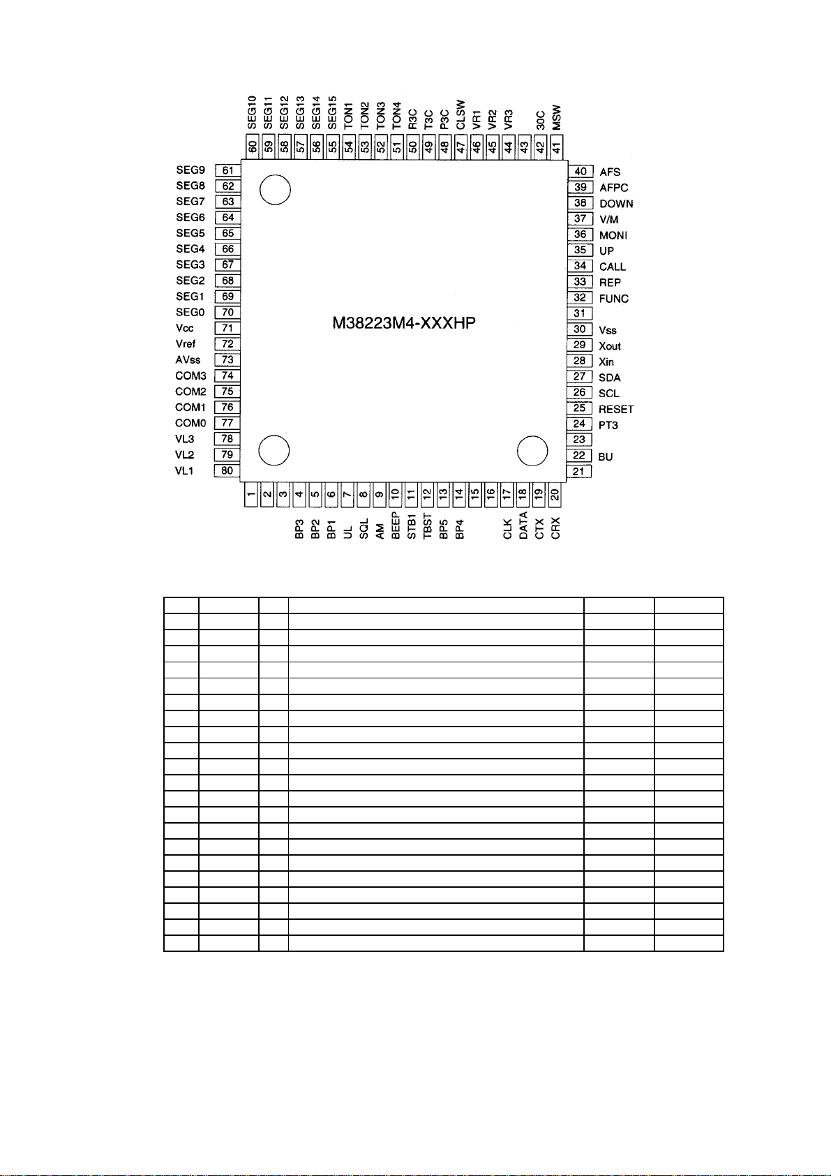
3) CPU Terminal Functions: M38224M4HP (XA0535)
No. Signal I/
O
Function H L
1
2
3
4 BP3 I Band plan3 (analog input)
5 BP2 I Band plan2 (analog input)
6 BP1 I Band plan1 (analog input)
7 UL I PLL unlock sinal input (analog input) UNL
O
CK
8S
Q
L I Noise level input for squelch (analog input) S
Q
L
O
N
9AM
O
AM power for short wave (DJ-C1) AM
O
N
10 BEEP
O
Beep tone output
11 STB1
O
Strobe for PLL
12 TBST
O
Tone burst output
13 BP5 I Band plan5
14 BP4 I Band plan4
15
16
17 CLK
O
Serial clock output for PLL
18 DATA
O
Serial data output for PLL
19 CTX
O
Clone data transmission output
20 CRX I Clone data reception input Page 7
No. Signal I/
O
Function H L
21
22 BU I Backup sinal detection input BACKUP
23
24 PT3 I PTT key input
25 RESET I Reset Sinal input RESET
26 SCL
O
Serial clock for EEPR
O
M
27 SDA I/
O
Serial data for EEPR
O
M
28 Xin I Mainc lock input
29 Xout I Mainc lock output
30 Vss I CPU GND
31
32 FUNC I FUNC KEY input
O
N
33 REP I REP KEY input
O
N
34 CALL I CALL KEY input
O
N
35 UP I UP KEY input
O
N
36 M
O
Nl I M
O
NI KEY input
O
N
37 V/M I VF
O
/MR KEY input
O
N
38 D
O
WN I D
O
WN KEY input
O
N
39 AFPC
O
Audio power amprlfier switch
O
N
40 AFS
O
AF mute switch MUTE
No. Name I/
O
Function H L
41 MSW
O
Microphone mute switch MUTE
42 30C
O
3V power switch
O
N
43
44 VR3
O
Volume leve13
45 VR2
O
Volume leveI2
46 VR1
O
Volume levell
47 CLSW
O
Clone switch CL
O
NE
48 P3C
O
PLL power switch .
O
N
49 T3C
O
TX power switch
O
N
50 R3C
O
145 M band power switch (DJ-C1)
O
N
43C 430 M band power switch DJ-C4
O
N
51 T
O
N4
O
Tone output 4
52 T
O
N3
O
Tone output 3
53 T
O
N2
O
Tone output 2
54 T
O
Nl
O
Tone output 1
55 SEG15
O
LCD SEG15
56 SEGl4
O
LCD SEG14
57 SEG13
O
LCD SEG13
58 SEG12
O
LCD SEG12
59 SEG11
O
LCD SEG11
60 SEG10
O
LCD SEG10
61 SEG9
O
LCD SEG9
62 SEG8
O
LCD SEG8
63 SEG7
O
LCD SEG7
64 SEG6
O
LCD SEG6
65 SEG5
O
LCD SEG5
66 SEG4
O
LCD SEG4
67 SEG3
O
LCD SEG3
68 SEG2
O
LCD SEG2
69 SEG1
O
LCD SEG1
70 SEG0
O
LCD SEG0
71 Vcc I Power supply termina 13V
72 Vref I A/D reference level 3V
73 AVss I CPU A/D GND
74 C
O
M3
O
LCD C
O
M3
75 C
O
M2
O
LCD C
O
M2
76 C
O
M1
O
LCD C
O
M1
77 C
O
M0
O
LCD C
O
M0
78 VL3 I LCD power
79 VL2 I LCD power
80 VL1 I LCD power Page 8