DR138
5
COMPARATOR
PHASE CHARGE
PUMP
U205:PLLIC
REF OSC
I/N
I/M
PLLDATA
LPF
Q210
TXVCO
Q218
BUFF AMP
Q209
19.200MHz
Q201,Q219
T/R SW
.
RXVCO
Q217
RF amplifiers
AMP
P45(CPU)
D219,D222
D217,D220
5KHz/6.25KHz
5KHz/6.25KHz
CIRCUIT DESCRIPTION
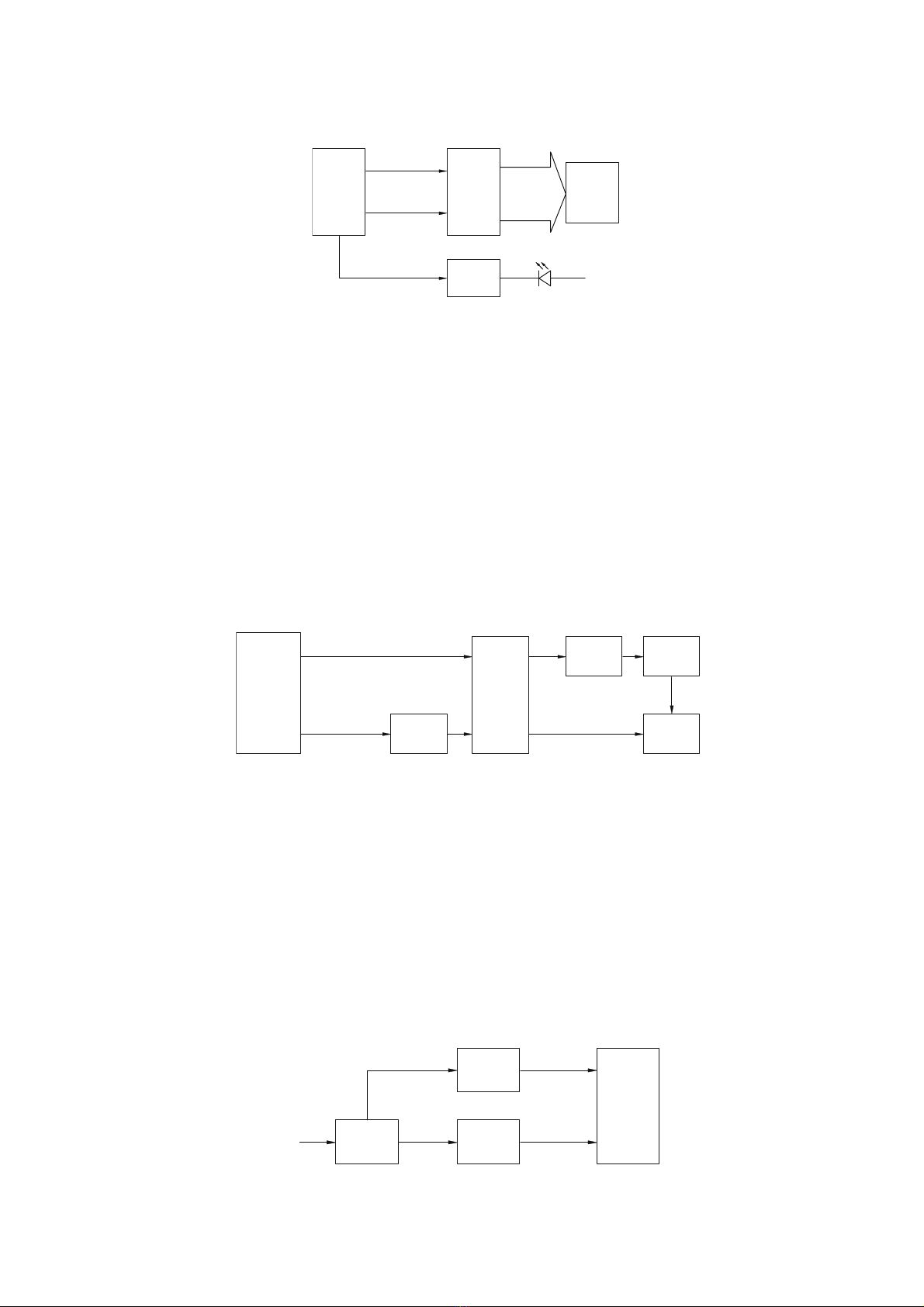
Squelch Circuit
The detection output from the FM IF IC (U200) passes through a noise amplifier (U202 B/2) to detect
noise. A voltage is applied to the CPU (U2). The CPU controls squelch according to the voltage (SQIN)
level. The signal from the RSSI pin of U200 is used for S-meter. The electric field strength of the receive
signal can be known before the SQIN voltage is input to the CPU, and the scan stop speed is improved.
Fig. 5 Squelch Circuit
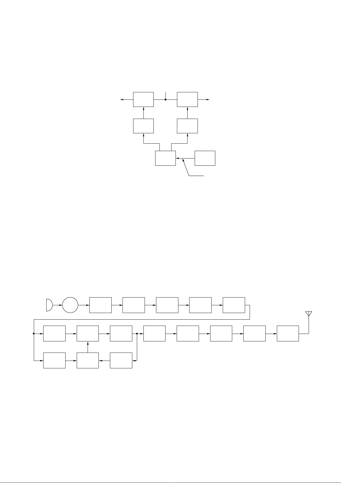
PLL frequency synthesizer
The PLL circuit generates the first local oscillator signal for reception and the RF signal for transmission.
PLL
The frequency step of the PLL circuit is 5 or 6.25kHz. A 19.200MHz reference oscillator signal is divided
at U205 by a fixed counter to produce the 5 or 6.25kHz reference frequency. The voltage controlled
oscillator (VCO) output signal is buffer amplified by Q210, then divided in U205 by a dualmodule
programmable counter. The divided signal is compared in phase with the 5 or 6.25kHz reference signal in
the phase comparator in U205. The output signal from the phase comparator is filtered through a low-pass
filter and passed to the VCO to control the oscillator frequency. (See Fig. 6.)
VCO
The operating frequency is generated by Q218 in transmit mode and Q217 in receive mode. The
oscillator frequency is controlled by applying the VCO control voltage, obtained from the phase
comparator, to the varactor diodes (D219 and D222 in transmit mode and D217 and D220 in receive
mode). The TX/RX pin is set high in receive mode causing Q202 and Q219 to turn Q218 off, and turn
Q217 on. The TX/RX pin is set low in transmit mode. The outputs from Q217 and Q218 are amplified by
Q209 and sent to the RF amplifiers. (See Fig. 6.)
Fig. 6 PLL circuit
UNLOCK Circuit
During reception, the RXC signal goes high, the TXC signal goes low, and Q108 turns on. Q101 turns
on and a voltage is applied to (8R). During transmission, the RXC signal goes low, the TXC signal goes
U200
SYSTEM
CPU
U2
NOISE AMP
U202
IF
SQ
RSSI
SQIN
RSSI
Downloaded from www.g7syw.com