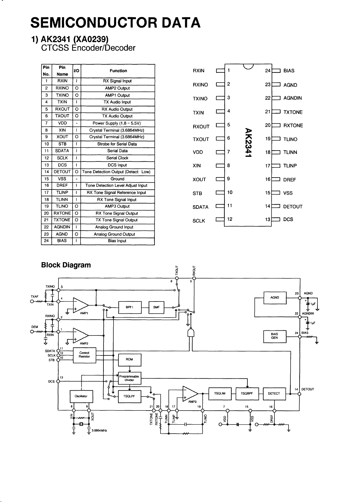
Alinco DR-130 User manual

DR-130
Service Manual
CONTENTS
SPECIFICATIONS
1)
General
2
PARTS LAST
2)
Transmitter
2
MAIN Unit
22-23
3)
Receiver
2
CPU Unit
24
CIRCUIT DESCRIPTION
VCO Unit
25
1)
Receiver System
3
SP Unit
25
2)
Transmitter System
4
EJ19u.
25
3)
PLL Circuit
4
Mechanical Parts
25
4)
Terminal Function of Microprocessor
5 - 7
Others
25
5)
Terminal Connection of Microprocessor
8
Packing..
25
SEMICONDUCTOR DATA
EJ20u
26
1)
AK2341
9
EMS-5A
26
2)
AN78LO5M
10
EMS-11
26
3)
AN8010M
10
ADJUSTMENT
4)
BU4052BF
10
1) Required Test Equipment.
27
5)
LR408721
11
2) Adjustment for DR-130
28~29
6)
M5218FP
11
3) Adjustment Points
30
7)
M56760FP
12
4) Adjustment Quick Reference
30
8)
MC7808CT
13
CIRCUIT DIAGRAM
9)
RH5VA32AA-T1
13
1) EMS-5A
31
10)
RH5VA45AA-T1
13
2) EMS-11
31
11)
S-AV17
14
3) Main Unit (T/E/EZ/EA/TA)
32
12)
TK10487MTR
15
4) Main Unit (TEl1/TE2)
33
13)
AT24CO2N-10SI-2.7
15
5) CPU Unit
34
14)
AT24CO8-10SI-2.7
15
PC BOARD VIEW
15)
uPC1241H
16
1) Main Unit Side A
35
16)
Transistor, Diode and LED Outline Drawings
16
2) Main Unit Side B
36
17)
LCD Connection
17
3) CPU Unit Side A.
37
EXPLODED VIEW
4) CPU Unit Side B
37
1)
Bottom View
18
5) VCO Unit Side A
38
2)
LCD View
18
6) VCO Unit Side B
38
3)
Top, Front View 1
19
BLOCK DIAGRAM
39
4)
Top, Front View 2
20
VERSION TABLE
21
ALINCO INCORPORATED
TWIN 21 M.I.D. TOWER BUILDING 23F, 1-61, 2-CHOME,
SHIROMI CHUO-KU , OSAKA, 540-8580 JAPAN
Tel (81)6-6946-8150 fax (81)6-6946-8175
e-mail: [email protected]

SPECIFICATIONS
1) General
Frequency Coverage: RX: 136.000 ~ 174.000MHz (T version)
TX: 144.000 ~ 148.000MHz (T version)
RX: 144.000 ~ 146.000MHz (E/EZ version)
TX: 144.000 ~ 146.000MHz (E/EZ version)
RX: 130.000 ~ 174.000MHz (EA/TA version)
TX: 130.000 ~ 174.000MHz (EA/TA version)
RX: 136.000 ~ 155.000MHz (TE1 version)
TX: 136.000 ~ 155.000MHz (TE1 version)
RX: 150.000 ~ 174.000MHz (TE2 version)
TX: 150.000 ~ 174.000MHz (TE2 version)
Frequency Resolution: 5, 10, 12.5, 15,20,25kHzsteps
Antenna Impedance: 50 ohm unbalanced
Power Supply Requirements
:
DC 13.8 +/-10% Volts DC
Current Drain at l3.8V Receiving: Squelched less than 800mA
Transmitting: High/10.0A (approx.)
Low/3.5A (approx.)
Dimensions: 140mm(W) x 40mm(H) x 154mm(D)
Weight: 0.86kg (approx.)
2) Transmitter High: 50Watts (DR-130T/E)
Output Power: High: 35Watts (DR-130TE1/2)
High:10Watts (DR-130EZ)
Low: 5Watts (Approx.)
Emission Mode: F3E(FM)
Modulation System: Variable Reactance Frequency Modulation
Max. Frequency Deviation: +/ -5kHz (Wide Version)
+/ -2.5kHz (Narrow Version)
Spurious Emission: -60dB or below carrier
Microphone: Electret Condenser Microphone
Operating Mode: Simplex/Semi-Duplex
Offset : 0ffset from 0 to 15.995MHz
3) Receiver
Receiving System: Superheterodyne Dual Conversion
Intermediate Frequency: 1stIF: 17.2MHz
2nd lF: 455kHz
12dB SINAD less than -l6dBu (144.000MHz ~ 147.995MHz)
Sensitivity: More than +/-6kHz at -6dB (Wide Version)
Selectivity: Less than +/-15kHz at -60dB (Wide Version)
Audio Power Output: More than 2.5W 10% Distortion
Speaker Impedance: 8 ohm Page-2

CIRCUIT DESCRTPTION
1) Receiver System
1. Front End The signal from the antenna is passed through a low-pass filter and input to
the voltage step up circuit consisting Of L14. The signal from L14 is led to
the gate of Q1. D19 is the diode limiter circuit against the excessive input
power of more than 20dBm. Q1 is the FETwhich has two gates. The
voltage of the gate 2 is set higher to get the high gain and sensitivity. The
signal from Q1 is led to the triple band pass filter (L4, L5, L6), and gets the
high image rejection ratio.
2. Mixer Circuit The signal from the triple band pass filter is converted into the first lF signal
of 17.2MHz. The receiving signal is led to the gate 1 of Q2, and the first
local oscillator signal is led to the gate 2 of Q2. To get the high conversion
gain, the local oscillator signal voltage is set to about 1V. To reduce the
high adjacent channel interference, the band width of the FL2 is set to
20kHz. The signal from FL2 is amplified by Q8, and input to FM IF system
IC3 of TK10487.
3. lF Circuit The TK10487 has the second local oscilltor circuit, mixer circuit, detector
circuit, squelch circuit, and so on. Pin1 and 2 are the terminals of the crystal
oscillator circuit. Pin2 (emitter) is connected to the ground via the resister
R3 to prevent the oscillator from decreasing the power at the low tempera-
ture. Pin4 of IC3 is connected to FL1 directly because the matching resistor
for ceramic filter is built-in. The quadrature circuit (pin10 of IC3) is con-
nected to the ceramic resonator X2 for the temperature stability and good
quality. The signal from pin11 of IC3 is connected to the LPF. The detected
AF signal, which has flat frequency characteristics, is led to the control unit
and used as both squelch signal and tone squelch signal. De-emphasis
circuit consists of R31, R32, C26 and C27. The LPF amplifier consisting of
Q5 and Q6 is located far away from the VR in the control unit, so it outputs
the high voltage signal to prevent S/N from the deterioration. The squelch
switch circuit consists of Q4 and Q16, and switches on/off at the point where
there is no voltage to prevent from the switching noise. The S meter signal
from pin12 of IC3 is led to the CPU in the control unit after adjusting the level
at D20 and VR5. The S meter signal is thermal compensated by TH1 and
stabilized. The noise amplifier consists of pin13 and 14, the built-in OP
amplifier in IC3. The output signal of noise amplifier is amplified by Q14,
rectified by D5, and then led to the pin15 (hysteresis comparator input) of
IC3.
4. AF Circuit IC4 is about 5W audio power amplifier IC. When the capacity of pin1 in C16
is increased more, the output incidental noise becomes smaller. The high-
pitched tone becomes smaller at the same time, This radio's capacity of
C16 is determined considering the high-pitched tone.
Page-3

2) Transmitter System
1. Modulation Circuit
3) PLL Circuit
The microphone amplifier IC1 (IDC, LPF) consists of two operational amplifi-
ers. The signal from the microphone is led to pre-emphasis circuit consisting
of C36 and R47 and then to the limiter circuit. The limiter circuit uses the
saturation of the OP amplifier. The amplified signal is input to the low-pass
filter IC1A. The output signal from the microphone amplifier is passed
through variable resistors VR2 for modulatlon adjustment and input to the
VCO unit. Sub tone deviation is determined by R24, R25 and VR2. The
radio does not have the adjustment variable resistor for sub tone deviation.
2. TX Amp. Circuit
The signal from VCO is ampriied by TX, RX wide band LO amplifier Q19.
The signal from Ql9 is passed through the transmission/reception selector,
and amplified byQ20 and Q15. The PA unit is driven at 200mW driving
power.
3. PA Circuit IC5 is 50W powered amplifier module. The output power is controlled by
the voltage ofV1. The RF signal amplified 50W in PA is passed through D3
and three-stage transmission/reception low-pass filter, and input to the
antenna connector.
4. ALC Circuit The power detection circuit consisting of D17 and D18 rectifies the output
signal voltage. The detected DC voltage is led to the VR1 (power adjust
trimmer), and amplified by Q3, Q9 and Ql3. Output power is controlled by
voltage of V1 in lC5 and collector voltage of Ql5. When the temperature
goes up unusually, the power down circuit consisting of R101 and TH2
works to prevent the device from the destruction.
The VCO unit is designed for the PLL circuit, putting the VCO on one side,
and PLL circuit on the other side.
Q301 in the VCO is grounded using the gate oscmator, and its frequency
covers 134MHz to 174MHz without transmission/reception shift circuit.
lC301 is pulse swallow system based PLL IC with the built-in prescaler,
which synthesizes 150MHzlband signal.
The loop filter consisting of Q302 and Q303 is the active type.
Page-4

4) Terminal Function of Microprocessor
Port No. I/O Logic PinName Description
1 O SEG19 LCDSegment19 Output
2 O SEG20 LCDSegment20 Output
3 O SEG21 LCDSegment21 Output
4 O SEG22 LCDSegment22 Output
5 O SEG23 LCDSegment23 Output
6 I GND AnalogGround 0V
7 I Vref Reference Voltage Input 5V
8 I Vcc CPU Power Supply hnput 5V
9 O 1750_ ToneBurstOutput
10 O Clock BEEP BeepToneOutput
11 I Active Low MUP Channel Up Input (Microphone Control)
12 I Active Low MDN Channel Down Input (Microphone Control)
13 I NoUse EID
14 O Active Low SQL Squelch Control (L: Audio is off.)
15 O ActiveHigh MUT Microphone Mute (H: Mic Amp is off.)
16 I Active Low REl RotaryEncoder Input
17 O Clock TO3 ToneOutput
18 O Clock TO2 ToneOutput
19 O Clock TO1 ToneOutput
20 O Clock TO0 ToneOutput
21 I ActiveHigh XWR EEPROM Write Status External Input
22 I Active Low RE2 RotaryEncoder Input
23 O Active Low BPO Band Plan Detection Input (Common)
24 I Active Low TID Tone Unit Detection Input
25 I Active Low BU Back Up Signal Detection input
26 I GND Ground
27 l Active Low RST ResetInput
28 I Xin Crystal Oscillator Terminal (3.58MHz)
29 O Xout Crystal Oscillator Terminal (3.58MHz)
30 I GND Ground
31 I Active Low TDO CTCSS Tone Detection Output
32 O Active Hig
h
DTD For Trunking
33 O NoUse
34 I Active Low DD4 Band Plan 4 (V/U Selection)
35 I Active Low DD3 Band Plan 3 (445/435 Selection)
36 I Active Low DD2 Band Plan 2 (5k/12.5k Selection)
37 I Active Low DD1 Band Plan 1
38 I Active Low DD0 Band Plan 0
39 O Clock SCL Clock Output for EEPROM Page-5

Port No. I/O Logic PinName Description
40 I/O Clock SDA Data Output for EEPROM
41 O Clock CLK Clock Output
42 O Clock DAT DataOutput
43 O Clock ST1 Strobe Output for PLL IC
44 O Clock ST2 Strobe Output for CTCSS IC
45 I Active Low SFT Shift Key Input
46 I Active Hig
h
SD Signal Detection Input
47 O Active Hig
h
H/L Transmission Power (H: Low Power)
48 I Active Low V/M VFO/Memory Key Input
49 I Active Low CAL Call Key Input
50 I Active Low CTC CTCSS Mode Set Input
51 I Active Low REV Reverse Key Input
52 I Active Low FNC Function Key Input
53 I Active Low MHz MHzKeyInput
54 I Active Low PTT PTTKeyInput
55 I LV3 Power Supply Input for LCD
56 I LV2 Power Supply Input for LCD
57 I LV1 Power Supply Input for LCD
58 I COM0 LCD Common 0 Output
59 I COM1 LCD Common 1 Output
60 I COM2 LCD Common 2 Output
61 I No Use
62 O SEG00 LCD Segment 00 Output
63 O SEG01 LCD Segment 01 Output
64 O SEG02 LCD Segment 02 Output
65 O SEG03 LCD Segment 03 Output
66 O SEG04 LCD Segment 04 Output
67 O SEG05 LCD Segment 05 Output
68 O SEG06 LCD Segment 06 Output
69 O SEG07 LCD Segment 07 Output
70 O SEG08 LCD Segment 08 Output
71 O SEG09 LCD Segment 09 Output
72 O SEG10 LCD Segment 10 Output
73 O SEG11 LCD Segment 11 Output
74 O SEG12 LCD Segment 12 Output
75 O SEG13 LCD Segment 13 Output
76 O SEG14 LCD Segment 14 Output
77 O SEG15 LCD Segment 15 Output
78 I ActiveHigh UL UnlockInput
79 I Analog SM SignalMeterInput
80 O SEG18 LCD Segment 18 Output
Page-6

Page-8

Page-9

Page-10

Page-11

Page-12

Page-13

Page-14

Page-15

Page-16

Page-17


Page-19
FF0028
FM0152
ES0017
KS0041B
KZ0047AZ
FF0031

Page-20
FM0152
NK0009B
NK0010A
FP0034
SS0052B
FF0030

VERSION TABLE
1)CPU UNIT
W1 W2 W3/W4 R284 R294/R295 R286 R296 R297 CN204 IC208
T JP - - - 0 - - - UE0165 -
E JP JP - 0 0 - - - UE0165 -
EZ JP JP - - 0 - lK 1K - AT24CO8-10SI
EA - - - 0 0 - - - UE0165 -
TA - - - - 0 - - - UE0165 -
TE1 - - JP - - - - - UE0165 -
TE2 - - JP - - - - - UE0165 -
TX Free RX Free Tranking 12.5k/5k Tranking V/U
2) MAIN UNIT
C7 C43 C62 C63 C68 C71,7
4,75,7 C112 C139 C149
T/E/EZ/EA/TA 1000p 33p 47p 10u/16V 15p 47p 22p 22p -
TE1 - 33p 100p 100u/16V 22p 56p 22p 12p 0.01uF
TE2 - 47p 33p 100u/16V 10p 1000p 18p 10p 0.01uF
C150
153 154
155 156 C151 C152 D4 D11 12
13 16 D15 lC5 L4,5,6,14
T/E/EZ/EA/TA - - - - 1SV215 lSS355 S-AV7 QA0084
TE1 1000p 10u/20V 10u/35V lSS355 1SV215 lSS355 M67781L QA0084
TE2 1000p 10u/20V 10u/35V lSS355 1SV214 - M67781HQA0100
L12 P3 R43 R57 R101 R102 R111 R121 R122 R130 W5
T/E/EZ/EA/TA QKA35D - 47k 22 15k 1k 0 - - 47k -
TE1 QKA35D 0 47k 100 2.2k 4.7k - - 220 - JP
TE2 QKA45D 0 27k 100 2.2k 4.7k - 0 220 - JP
3) VCO UNIT C315 C331 C332 D304 R315 R316 R332 R333 R334
T/E/EZ/EA/TA 3p - - - 10k 100 - - -
TE1 3p 4700p 0.5p 1SV215 22k 56 8.2k 8.2k 220k
TE2 1p 4700p 0.5p 1SV215 22k 56 10k 8.2k 220k
Page-21
Other Alinco Radio manuals

Alinco
Alinco DJ-596T User manual

Alinco
Alinco DR-135 User manual

Alinco
Alinco DJ-493 User manual

Alinco
Alinco DR-138 User manual

Alinco
Alinco DR-1200T User manual

Alinco
Alinco DJ-V446 User manual

Alinco
Alinco DR-135T MkII User manual

Alinco
Alinco DJ-446 User manual

Alinco
Alinco DR-235 User manual

Alinco
Alinco DX-R8T User manual

Alinco
Alinco DR-235 User manual

Alinco
Alinco DJ-S17 E User manual

Alinco
Alinco DJ-C1 User manual

Alinco
Alinco DR-MD500 User manual

Alinco
Alinco DR-570T User manual

Alinco
Alinco DJ - C7 T User manual

Alinco
Alinco DR-635 User manual

Alinco
Alinco DR-1200T User manual

Alinco
Alinco DR-M03R User manual

Alinco
Alinco 135T User manual