Balluff BIS C-6002 User manual

1
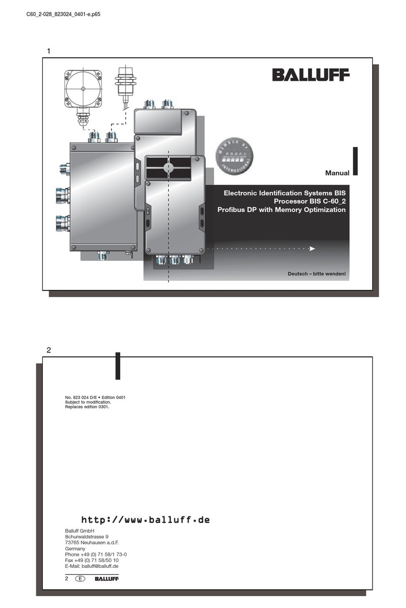
Electronic Identification Systems BIS
Processor BIS C-60_2
Profibus DP
Manual
Deutsch – bitte wenden!
C60_2-019_818217_0806-e.p65
2
No. 818 217 D/E • Edition 0806
Subject to modification.
Replaces edition 0608.
Balluff GmbH
Schurwaldstrasse 9
73765 Neuhausen a.d.F.
Germany
Phone +49 7158 173-0
Fax +49 7158 5010

3
3
english
Contents
Safety Considerations................................................................................................................. 4
Introduction, BIS C Identification Systems..............................................................................5-7
BIS C-60_2 Processor, Basic knowledge for application ........................................................ 8/9
BUS interface PROFIBUS-DP..............................................................................................10-12
Compatibility with BIS C-6_2 processor .................................................................................. 13
Function Description: Communication with the processor ................................................. 14
Input and Output Buffers ............................................................ 15/16
Output Buffer, configuration and explanation .............................17-20
Input Buffer, configuration and explanation ................................ 21-24
Parametering the BIS C-60_2 processor................................... 25-28
Processing data carriers ............................................................ 29-35
Examples for protocol sequence .............................................. 36-53
Read/Write Times ............................................................................................................... 54/55
LED Display ............................................................................................................................. 56
BIS C-6002 BIS C-6022
Mounting Head / Processor ..............................................................................57 .................. 75
Opening the Processor .....................................................................................58 .................. 76
Installing the connection cables / Mounting the PG connection .............. 59/60
Interface information / Wiring Diagrams ..................................................... 61-68 ............. 77-80
Changing the EEPROM .....................................................................................69 .................. 81
Technical Data ............................................................................................. 70-72 ............. 82/83
Ordering Information: Ordering Code / Accessory .................................... 73/74 .................. 84
Appendix, ASCII Table ............................................................................................................. 85
C60_2-019_818217_0806-e.p65
4
english4
Safety Considerations
Series BIS C-60_2 processors along with the other BIS C system components comprise an
identification system and may only be used for this purpose in an industrial environment in
conformity with Class A of the EMC Law.
Installation and operation should be carried out by trained personnel only. Unauthorized work
and improper use will void the warranty and liability.
When installing the processor, follow the chapters containing the wiring diagrams closely.
Special care is required when connecting the processor to external controllers, in particular
with respect to selection and polarity of the signals and power supply.
Only approved power supplies may be used for powering the processor. See chapter 'Techni-
cal Data' for details.
Prevailing safety regulations must be adhered to when using the identification system. In par-
ticular, steps must be taken to ensure that a failure of or defect in the identification system
does not result in hazards to persons or equipment.
This includes maintaining the specified ambient conditions and regular testing for functionality
of the identification system including all its associated components.
Should there ever be indications that the identification system is not working properly, it
should be taken out of commission and secured from unauthorized use.
This manual applies to processors in the series BIS C-6002-019-...-03-... and
BIS C-6022-019-050-03-....
Installation and
Operation
Use and Checking
Fault Conditions
Scope
Approved Operation
5
5
english
Principles
Introduction
BIS C Identification Systems
Applications
☞
This manual is designed to assist the user in setting up the control program and installing and
starting up the components of the BIS C Identification System, and to assure rapid, trouble-
free operation.
The BIS C Identification Systems belongs in the category of
non-contact systems for reading and writing.
This dual function permits applications for not only transporting information in fixed-program-
med Data carriers, but also for gathering and passing along up-to-date information as well.
If 2 read/write heads are connected to a BIS C-60_2 processor, both heads can be operated
independently of each other. This means for example that you can read a Data carrier from one
head while writing to another Data carrier at the other head.
Some of the notable areas of application include
– for controlling material flow in production processes
(e.g. in model-specific processes),
for workpiece conveying in transfer lines,
in data gathering for quality assurance,
for gathering safety-related data,
– in tool coding and monitoring;
– in equipment organization;
– in storage systems for monitoring inventory movement;
– in transporting and conveying systems;
– in waste management for quantity-based fee assessment.
C60_2-019_818217_0806-e.p65
6
english6
BIS C-3_ _BIS C-35_ BIS C-3_ _BIS C-65_
BIS C-670 BIS C-650
System Components The main components of the BIS C Identification Systems are:
–Processor,
–Read/Write Heads and
–Data carriers
Introduction
BIS C Identification Systems
PROFIBUS-DP
Data carriers BIS C-1_ _-...
Schematic
representation of an
Identification System
(example)
Processor BIS C-6002
with
adapter
Read/write
heads 1)
1) BIS C-3_ _ series, except BIS C-350 and -352 2) only BIS C-350 or -352
Read/write
head 2)
Processor BIS C-6002
with
adapter
Processor BIS C-6002
with
read/
write head
Configuration with
BIS C-6002
processor

7
7
english
BIS C-3_ _BIS C-3_ _ BIS C-3_ _BIS C-3_ _
Introduction
BIS C Identification Systems
Read/write heads1)
Schematic
representation of an
identification system
(example) 1) BIS C-3_ _ series, except BIS C-350 and -352
PROFIBUS-DP
Data carriers BIS C-1_ _-...
Configuration with
BIS C-6022
processor
Processor BIS C-6022
version -050
Processor BIS C-6022
version -050
C60_2-019_818217_0806-e.p65
8
english8
Selecting System
Components
The BIS C-6002 processor has a plastic housing. Depending on the version, connections are
made either through a terminal strip, with the cable secured using a PG fitting, or via round
connectors. A single read/write head from BIS C-65_ series can be directly mounted to the
processor, which creates a compact unit. If the BIS C-650 adapter is attached instead of the
BIS C-65_ read/write head, two read/write heads may be cable connected. If the BIS C-670
adapter is attached, one read/write head may be cable connected.
The BIS C-6022 processor has a metal housing. Connection is made through round connec-
tors. Two read/write heads can be cable connected to the BIS C-6022 processor.
Series BIS C-60_2 processors have in addition a digital input. The input has various functions
depending on the configuration (see Parametering).
Whether the compact version of the processor with integrated read/write head makes sense
or whether the external solution is preferred depends primarily on the spatial arrangement of
the components. There are no functional limitations. All read/write heads are suitable for both
static and dynamic reading. Distance and relative velocity are based on which Data carrier is
selected. Additional information on the read/write heads in series BIS C-65_ and series
BIS C-3_ _ including all the possible Data carrier/read-write head combinations can be found
in the manuals for the respective read/write heads.
The system components are electrically supplied by the processor. The Data carrier repre-
sents an free-standing unit and needs no line-carried power. It receives its energy from the
read/write head. The latter constantly sends out a carrier signal which supplies the code head
as soon as the required distance between the two is reached. The read/write operation takes
place during this phase. Reading and writing may be dynamic or static.
BIS C-60_2 Processor
Basic knowledge for application

9
9
english
BIS C-60_2 Processor
Basic knowledge for application
The processor writes data from the host system to the Data carrier or reads data from the
tag through the read/write head and prepares it for the host system. Host systems may
include:
–a host computer (e.g. industrial PC) or
–a programmable logic controller (PLC)
When sending data between the read/write head and the Data carrier a procedure is re-
quired for recognizing whether the data were correctly read or written.
The processor is supplied with standard Balluff procedure of double reading and compar-
ing. In addition to this procedure a second alternative is available: CRC_16 data checking.
Here a test code is written to the Data carrier, allowing data to be checked for validity at
any time or location.
Advantages of CRC_16 Advantages of double reading
Data checking even during the non-active phase
(CT outside read/write head zone).
No bytes on the data carrier need to be
reserved for storing a check code.
Shorter read times since each page is read only
once.
Shorter write times since no CRC needs to be
written.
Since both variations have their advantages depending on the application, the user is free
to select which method of data checking he wishes to use (see Parametering on 26).
It is not permitted to operate the system using both check procedures!
Control Function
Data checking
☞
C60_2-019_818217_0806-e.p65
10
english10
Communication between the BIS C-60_2 processor and the host system is via PROFIBUS-DP.
The PROFIBUS-DP system consists of the components:
– the bus master and
– the bus modules/slaves (here the BIS C-60_2 processor).
Important hints for use with PLC:
In some control systems the PROFIBUS-DP data area is not synchronously transmitted with the
updating of the input/output content. If more than 2 bytes of data are sent, a mechanism must
be used which guarantees that the data in the PLC and the data in the BIS C are always identi-
cal!
1st alternative: Synchronous data transmission as a setting on the Master
In this method the bus Master ensures that all the data necessary for the respective Slave are
always sent contiguously. There is usually a special software function in the PLC which likewise
controls access between the PLC and bus Master so that data are always sent contiguously.
2nd alternative: Set 2nd bit header
Data exchange between PLC and BIS is controlled by the so-called bit header. This is always
the first byte of the respective read/write head in the data buffer. This bit header exists both in
the input range (data from BIS to the PLC) and in the output range (data from the PLC to the
BIS). lIf this bit header is also sent as the last byte, a comparison of these two bytes can be
used to guarantee the consistency of the transmitted data.
In this method the PLC cycle is unaffected nor is the bus access time changed. All that is
required is that a byte in the data buffer be used for the 2nd bit header instead of for user data.
This 2nd alternative is the Balluff recommended setting (factory default).
PROFIBUS-DP
☞
BUS interface PROFIBUS-DP

11
11
english
Station Address
For the correct parametering of the bus master as per type, a diskette, containing the unit’s
master data in the form of a GSD file is included with the BIS C-60_2 processor.
The Processor BIS C-60_2 is delivered with the station address 126. This has to be set indi-
vidually before using in a bus system. See information on 12.
An input buffer and an output buffer are used for the data exchange with the control system.
The size of these buffers has to be configured via the master.
The possible settings are entered in the GSD file (and Type file). A minimum of 4 and a maxi-
mum of 128 bytes can be accommodated. However, it must be an even number.
Besides, in the case of the BIS C-60_2 processor, there are 6 further bytes (User-Parameter
Bytes) which have to be set while parametering. The significance of the 6 bytes for para-
metering is described starting from 25.
The preset is stored in the GSD file.
Input/Output Buffer
Unit's Master Data
Parametering Bytes
User-Parameter Bytes
☞
☞
BUS interface PROFIBUS-DP
C60_2-019_818217_0806-e.p65
12
english12
Station Address
setting
The station address under which the unit is accessed on the bus can be assigned through the
slide switch S1. Each address shall be assigned only once.
The slide switch S1 is binary coded. The setting of the station address is carried out according
to the scheme shown in the table. Switch position: no = left, yes = right.
The address 85 is set in the following figure.
➪
no yes
To open the cover of the processor, see 58 for BIS C-6002 or 76 for BIS C-6022.
BUS interface PROFIBUS-DP
Slide switch S1
(with cover removed)
Station
Address
Slide switch S1
7654321
26252423222120
0notallowed
1 nonononononoyes
2 nononononoyesno
3 nononononoyesyes
4 nonononoyesnono
5 nonononoyesnoyes
...
85 yes no yes no yes no yes
...
123 yes yes yes yes no yes yes
124 yes yes yes yes yes no no
125 yes yes yes yes yes no yes
126 yes yes yes yes yes yes no
127 not allowed

13
13
english
Setting compatibility Slide switch S1 is used to set compatibility with the BIS C-602 and BIS C-622 processors.
If the BIS C-60_2 processor is set to be compatible with the BIS C-602 or BIS C-622, all set-
tings for data exchange must be made as described in the sections on parametering, function
description, protocol sequence and LED display in the user’s manual for the BIS C-6_2 proces-
sor! This user’s manual can be mailed on request, or you may download it from the Internet at
www.balluff.de.
Slide switch S1
(with cover removed)
➪
no yes
Key: no = switch left
yes = switch right
In the illustration compatibility with the BIS C-6_2 is not set.
To open the cover of the BIS C-6002 processor, see 58,
and for BIS C-6022 see 76.
Slide switch S1
8 compatible with
yes BIS C-6_2
no BIS C-60_2
☞
Compatibility with BIS C-6_2 processor
C60_2-019_818217_0806-e.p65
14
english14
Function Description
Communication with the processor
Communication between the host system and the processor takes place using a fixed proto-
col sequence. Data integrity from the control to the processor and vice-versa is indicated by a
control bit. This bit is used to implement a handshake between the control and the processor.
Following is a simplified representation of the sequence of a job sent from the control to the
processor:
1. The control sends a command designator to the processor together with the associated
command parameters and sets a bit (AV bit). This bit indicates to the processor that the
transmitted data are valid and that the job is now beginning.
2. The processor takes the job and sets a bit (AA bit), which indicates this to the control.
3. If an additional exchange of data between the control and the processor is required to
carry out the job, each uses a bit (TI bit and TO bit) to indicate that the control / processor
is now ready for additional data exchange or has accepted the received data.
4. Once the processor has carried out the job correctly, it sets a bit (AE bit).
5. Once the control has accepted all the important data, it indicates this to the processor by
resetting the bit that was set at the beginning (AV bit).
6. The processor now in turn sets all the control bits that were set during the sequence
(AA bit, AE bit) and is ready for the next job.
Please see also
29...35 and the
examples on
36...53.
Basic Procedure

15
15
english
Input and Output
Buffers
In order to transmit commands and data between the BIS C-60_2 and the host system, the
latter must prepare two fields. These two fields are:
–the output buffer
for the control commands which are sent to the BIS Identification System and
for the data to be written.
–the input buffer
for the data to be read and
for the designators and error codes which come from the BIS Identification System.
The possible setting values are stored in the GSD file.
The buffer size can be selected between 4 and 128 bytes in steps of 2 bytes. This must be
given by the master during parametering. The total buffer size is divided into 2 ranges:
Buffer range 1 for Read/Write Head 1; size is specified in paramter byte 6.
Buffer range 2 for Read/Write Head 2; size = total buffer size – buffer size of Read/Write
Head 1. See 16 for example.
If a buffer size of less than 6 bytes (8 bytes with double bit header) is set for a read/write head, a
read/write request can be carried out without specifying the start address and the number of
bytes. Automatic reading for Codetag-Present (see 30) remains active. This permits fast
reading of small data quantities without placing an unnecessary load on the bus.
Buffer size – 1 = number of bytes read without double bit header;
Buffer size – 2 = number of bytes read with double bit header.
☞
Function Description
Input and Output Buffers
Please note the
basic procedure on
14 and 29...35
and the examples on
pages 36...53.
C60_2-019_818217_0806-e.p65
16
english16
Function Description
Input and Output Buffers
☞
Example: The 82 bytes for the total buffer need to be distributed. An input/output buffer of
46 bytes is assigned to Read/Write Head 1. This results in an input/output buffer of 36 bytes
for Read/Write Head 2.
Procedure: The buffer size for Read/Write Head 1 is set to 46 bytes. This means using the
parameter byte 6 to enter Hex value 2E (corresponds to 46 decimal), which corresponds to
binary 00101110.
PLC Organisation: The buffer range starts at input byte IB 32 and output byte OB 32.
Result:
Read/Write Head 1: Subaddress 00 IB 32 and OB 32
(R/W 1) Input buffer IB 32 to IB 77
Output buffer OB 32 to OB 77
Read/Write Head 2: Subaddress 00 IB 78 and OB 78
(R/W 2) Input buffer IB 78 to IB 113
Output buffer OB 78 to OB 113
IB 0 / OB 0 PLC buffer
Buffer for R/W 1
Buffer for R/W 2
Input and Output
Buffers
(continued)
Note that these buffers can be in two different
sequences depending on the type of control.
The following description is based on sequence 1!
Sequence 1 Sequence 2
Subaddress 00 Subaddress 01
01 00
02 03
03 02
04 05
05 04
06 07
07 06
Please note the
basic procedure on
14 and 29...35
and the examples on
pages 36...53.

17
17
english
The last byte can be arranged as a 2nd bit header through parametering (default).
Function Description
Output buffer, configuration and explanation
BitNo.765432 10
Subaddress
00Hex = Bit Header CT TI HD GR AV Bit Name
01Hex Command Designator or Data
02Hex Start Address (Low Byte) or Program No. or Data
03Hex Start Address (High Byte) or Data
04Hex No. of Bytes (Low Byte) or Data
05Hex No. of Bytes (High Byte) or Data
06Hex Data
... Data
Last Byte 2nd Bit Header (as above) or Data
Sub- Bit Meaning Function Description
address Name
00Hex CT Data carrier type Select Data carrier type: for Data carrier type:
Bit Header 0 32 Byte block size BIS C-1_ _-02, -03, -04, -05
1 64 Byte block size BIS C-1_ _-10, -11, -30
TI Toggle-Bit In Shows during a read action that the controller is ready
for additional data.
HD Head select for Head 1 for Head 2
0 Select Head 1.1 Select Head 2.1
1 Select Head 1.2 Select Head 2.2
(only in conjunction with Adapter 655)
(continued next )
Configuration of the
output buffer for one
(1) read/write head
Description of
Output Buffer
Please note the
basic procedure on
14 and 29...35
and the examples on
pages 36...53.
C60_2-019_818217_0806-e.p65
18
english18
Function Description
Output buffer, configuration and explanation
Sub- Bit Meaning Function Description
address Name
00Hex GR Ground state Causes the BIS system to go to the ground state
Bit Header for the respective read/write head.
Any pending command is cancelled.
AV Command Signals the identification system that a command
for the respective read/write head is present.
Sub- Meaning Function Description
address
01Hex Command designator
00Hex No command present
01Hex Read Data carrier
02Hex Write to Data carrier
06HEX Store program in the EEPROM for the Mixed Data Access
function
07HEX Store the start address for the Auto-Read function in the
EEPROM
11HEX Copying from Head 1 to Head 2
12HEX Initialize the CRC_16 data check
21HEX Read for Mixed Data Access function
(corresponding to the program stored in the EEPROM)
22HEX Write for Mixed Data Access function
(corresponding to the program stored in the EEPROM)
or Data for writing to the Data carrier
or Program data for writing to the EEPROM.
(continued next )
Description of
Output Buffer
(continued)
Please note the
basic procedure on
14 and 29...35
and the examples on
pages 36...53.

19
19
english
Function Description
Output buffer, configuration and explanation
Description of
Output Buffer
(continued)
Sub- Meaning Function Description
address
02Hex Start address Address at which reading from or writing to the Data carrier
(Low Byte) begins.
(The Low Byte includes the address range from 0 to 255).
or Start address Address for the Auto-Read function, starting at which the code
(Low Byte) tag is to be read. The value is stored in the EEPROM. (The Low
Byte covers the address range from 0 to 255).
or Program No. Number of the program to be stored in the EEPROM in
conjunction with command ID 06Hex for Mixed Data Access
function (values between 01Hex and 0AHex are allowed!).
or Program No. Number of the program stored in the EEPROM for read or write
operations in conjunction with command ID 21Hex or 22Hex for the
Mixed Data Access function.
or Data for writing to the Data carrier
or Program data for writing to the EEPROM.
03Hex Start address Address for reading from or writing to the Data carrier (the High
Byte (High Byte) is additionally used for the address range from 256 to 8,191).
or Start address Address for the Auto-Read function, starting at which the code
(High Byte) tag is to be read. The value is stored in the EEPROM (the High
Byte is also required for the address range from 256 to 8,191).
or Data for writing to the Data carrier
or Program data for writing to the EEPROM.
(continued next )
Please note the
basic procedure on
14 and 29...35
and the examples on
pages 36...53.
C60_2-019_818217_0806-e.p65
20
english20
Function Description
Output buffer, configuration and explanation
Description of
Output Buffer
(continued)
Sub- Meaning Function Description
address
04Hex No. of bytes Number of bytes to read or write beginning with the start address
(Low Byte) (the Low Byte includes from 1 to 256 bytes).
or Data for writing to the Data carrier
or Program data for writing to the EEPROM.
05Hex No. of bytes Number of bytes to read or write beginning with the start address
(High Byte) (the High Byte is additionally used for the range between 257 and
8,192 bytes).
or Data for writing to the Data carrier
or Program data for writing to the EEPROM.
06Hex Data for writing to the Data carrier
or Program data for writing to the EEPROM.
... Data for writing to the Data carrier
or: Program data for writing to the EEPROM.
Last byte
2nd Bit header The data are valid if the 1st and 2nd bit header are identical.
or Data for writing to the Data carrier
or Program data for writing to the EEPROM.
Please note the
basic procedure on
14 and 29...35
and the examples on
pages 36...53.

21
21
english
Function Description
Input buffer, configuration and explanation
Configuration of the
input buffer for one
(1) read/write head
The last byte can be arranged as a 2nd bit header through parametering (default).
Sub- Bit Meaning Function Description
address Name
00Hex BB Ready The BIS Identification System is in the Ready state.
Bit Header HF Head Error Cable break from read/write head or
no read/write head connected.
TO Toggle-Bit Out for read: BIS has new/additional data ready.
for write: BIS is ready to accept new/additional data.
(continued on next )
BitNo.76543210
Subaddress
00Hex = Bit Header BB HF TO IN/KN AF AE AA CP Bit Name
01Hex Error Code or Data
02Hex Data
03Hex Data
04Hex Data
05Hex Data
06Hex Data
... Data
Last byte 2nd Bit Header
(as above) or Data
Description of
Input Buffer
Please note the
basic procedure on
14 and 29...35
and the examples on
pages 36...53.
C60_2-019_818217_0806-e.p65
22
english22
Function Description
Input buffer, configuration and explanation
Description of
Input Buffer
(continued)
Sub- Bit Meaning Function Description
address Name
00Hex (continued)
Bit Header IN/KN Use the same bit in the bit header. Either IN or KN
may be displayed. Therefore select either Parameter
4th byte, bit 7 = 1 or Parameter 4th byte, bit 6 = 1.
(see 27)
IN Input If the parameter is 4th byte, bit 7 = 1 and 4th byte,
bit 6 = 0, this bit indicates the status of the input.
KN Head No. If the parameter is 4th byte, bit 6 = 1 and 4th byte,
bit 7 = 0, this bit indicates the selected head.
AF Command Error The command was incorrectly processed or aborted.
AE Command end The command was finished without error.
AA Command start The command was recognized and started.
CP Codetag Present Data carrier present within the active zone of the
read/write head.
In addition to the CP bit, the output signal CT-Present is available. This allows
you to process the presence of a Data carrier directly as a hardware signal.
Sub- Meaning Function Description
address
01Hex Error code Error number is entered if command was incorrectly processed
or aborted. Only valid with AF bit!
00Hex No error.
01Hex Reading or writing not possible because no Data carrier is present
in the active zone of a read/write head.
(continued on next )
Please note the
basic procedure on
14 and 29...35
and the examples on
pages 36...53.

23
23
english
Sub- Meaning Function Description
address
01Hex Error code (continued)
02Hex Read error.
03Hex Data carrier was removed from the active zone of the read/write
head while it was being read.
04Hex Write error.
05Hex Data carrier was removed from the active zone of the read/write
head while it was being written.
07Hex AV bit is set but the command designator is missing or invalid.
or Number of bytes is 00Hex.
09Hex Cable break to select read/write head, or head not connected.
0CHex The EEPROM cannot be read/programmed.
0DHex Faulty communication with the Data carrier.
Note: Verify installation criteria or distance between data carrier
and read/write head.
0EHex The CRC of the read data does not coincide with the CRC of
the Data carrier.
0FHex Contents of the 1st and 2nd bit header (1st and last bytes) of
the output buffers are not identical (2nd bit header must be
served).
11Hex Invoking a function that is not possible, since the processor is in
“compatible with BIS C-6_2” mode.
12Hex Copying is not possible, since a command is already started
on Head 2.
or: Data Data which was read from the Data carrier.
(continued on next )
Function Description
Input buffer, configuration and explanation
Description of
Input Buffer
(continued)
Please note the
basic procedure on
14 and 29...35
and the examples on
pages 36...53.
C60_2-019_818217_0806-e.p65
24
english24
Function Description
Input buffer, configuration and explanation
Description of
Input Buffer
(continued)
Sub- Meaning Function Description
address
02Hex Data Data which was read from the Data carrier.
... Data Data which was read from the Data carrier.
Last byte
2nd Bit header The data are valid if the 1st and 2nd bit headers are in
agreement.
or Data Data which was read from the Data carrier.
Please note the
basic procedure on
14 and 29...35
and the examples on
pages 36...53.

25
25
english
Function Description
Parametering the BIS C-60_2 processor
Parameters,
Overview
There are 6 user parameter bytes stored on the Profibus master that can be used to activate
and deactivate various functions. Setting is done directly by linking a device to the Profibus
master. The parameter default settings are stored in the GSD file.
– CRC_16 data check:
If this function is activated, the correctness of the read or written data is ensured by a
CRC_16 data check (see 9).
– Simultaneous data transmission for both read/write heads:
With simultaneous data transmission shorter read/write times can be achieved depending
on the amount of data to be read/written and the type of controller.
– Dynamic operation on read/write head 1 or 2:
If dynamic operation is parametered, a read/write job can be sent even though there is no
Data carrier in the active zone of the head. As soon as a Data carrier passes by the head,
the command is immediately carried out.
– "Auto-Read” for read/write head 1 or 2:
If this function is activated, the processor reads out the first (max. 31) bytes from the Data
carrier starting at a defined start address as soon as the tag enters the active zone of the
read/write head. The start address must first have been stored in the processor’s EEPROM
with the command ID 07Hex.
– 2nd bit header at end of in- and output buffer:
The 2nd bit header (factory setting) prevents data from being accepted by the bus as long
as it is not fully updated.
– Display state of the digital input in the bit header of the input buffer:
If this function is activated, the IN-bit displays the state of the digital input of the processor:
IN = 0 →digital input low; IN = 1 →digital input high
– Reset BIS C-60_2 processor through the digital input:
If this function is activated, the processor is reset when the digital input is set to high.
Please note the
basic procedure on
14 and 29...35
and the examples on
pages 36...53.
C60_2-019_818217_0806-e.p65
26
english26
Parametering Bytes
User-Parameter Bytes For parametering all 6 bytes must always be transferred in Hex. Only the bits mentioned
may be changed. No guaranty will be given for the proper functioning of the
BIS C-60_2 if any of the other bits are changed.
The default values (factory setting) for the 6 bytes are:
1st byte 2nd byte 3rd byte 4th byte 5th byte 6th byte
Hex 00 80 00 82 00 02
Binary 00000000 10000000 00000000 1000001000000000 00000010
bit 6
bit 4 bit 7 bit 2 bit 4 bit 1...8
bit 5 bit 5 bit 8 bit 5
bit 8
The bits which serve for parametering have the following functions:
1st byte, bit 5 Activate CRC_16 data checking
2nd byte, bit 5 Dynamic mode on read/write head 1
(for effects on read/write times, see 54/55)
2nd byte, bit 4 Activate Auto-Read function starting at specified address after CT-
Present for Head 1 (the number of bytes read depends on the selected
buffer size minus bit headers for Head 1)
4th byte, bit 8 Arrange a 2nd bit header at the end of the input and output buffers
If this function is selected, then the minimum size of both buffers is 4 words (8 bytes) each.
Please note the basic procedure on 14 and 29...35 and the examples on pages 36...53.
Function Description
Parametering, Parametering Bytes
Bit state: 0 = no
1 = yes
These are used for
configuration:
Having the following
functions:
☞

27
27
english
4th byte, bit 7 Display state of the digital input in the bit header of the input buffers:
0 = no Input is Low: "IN" in the bit header of the input buffers = 0.
1 = yes Input is High: "IN" in the bit header of the input buffers = 1.
Important: „KN“ and „IN“ use the same bit in the bit header.
If the BIS C-655 adapter is connected for 2 x 2 heads, you must select 0 = no.
4th byte, bit 6 Select read/write adapter 2 Head/4 Head connection
0 = no Select this setting if no more than 2 read/write heads can be connected.
Standard configuration.
1 = yes Select this setting if the processor is being operated using the
BIS C-655 read head adapter and 2 x 2 heads.
Important: If 4th byte, bit 6 is set to 1 = yes, the setting 4th byte, bit 7 must be set to
0 = no.
4th byte, bit 2 Reset the BIS C-60_2 processor through the digital input:
0 = no Input is Low: Do not reset.
1 = yes Input is High: Reset.
5th byte, bit 8 Activate simultaneous data transmission for both read/write heads
5th byte, bit 5 Dynamic mode on read/write head 2
(for effects on read/write times, see 54/55)
5th byte, bit 4 Activate Auto-Read function for Head 2 starting at specified address
after CT-Present (the number of bytes read depends on the selected
buffer size minus bit headers for Head 2)
6th byte, bit 1...8 No. of bytes in input and output buffer which shall be used for
read/write head 1, see example on 16
Parametering Bytes
User-Parameter Bytes
(continued)
Function Description
Parametering, Parametering Bytes
Bit state: 0 = no
1 = yes
C60_2-019_818217_0806-e.p65
28
english28
The specification for the input and output buffer on the Master applies to both read/write
heads, i.e. this buffer must be divided for both heads. The specification is done in Hex
format and must be in a range between 02Hex and 80Hex (128 dec.).
If only one read/write head (Head 1) will be used, you may enter the same value here as for the
total buffer size. An entry of less than 2 bytes results in an undefined state.
Please note the basic procedure on 14 and 29...35 and the examples on pages 36...53.
☞
Parametering Bytes
User-Parameter Bytes
(continued)
Function Description
Parametering, Parametering Bytes

29
29
english
Reading and writing To carry out a read or write job, the Data carrier must be located in the active zone of the read/
write head.
A read/write job has the following sequence (see examples on 38ff):
1. The host sends to the output buffer:
– the command designator to subaddress 01Hex,
– the start address for reading or writing to subaddress 02HEX/03HEX,
– the number of bytes for reading or writing to subaddress 04HEX/05HEX,
– the CT bit in the bit header according to the Data carrier type (block size),
– and sets the AV bit in the bit header to high.
2. The processor:
– takes the request (AA bit in the bit header of the input buffer to high),
– begins to transport the data;
read = from data carrier to input buffer,
write = from output buffer to data carrier.
Larger data quantities are sent in blocks
(block size with 2nd bit header = buffer size – 2),
block size without 2nd bit header = buffer size – 1).
The toggle bits in the two bit headers are used as a kind of handshaking between the
host and the BIS C-60_2 processor.
3. The processor has processed the command correctly (AE bit in the bit header of the input
buffer). If an error occurred during execution of the command, an error number will be
written to subaddress 01Hex of the input buffer and the AF bit in the bit header of the input
buffer will be set.
Function Description
Processing data carriers
C60_2-019_818217_0806-e.p65
30
english30
Special
characteristics
Auto-Read
Function Description
Processing data carriers
Codetag Present As soon as the data carrier enters the active one of the read/write head, the processor indi-
cates this by setting the CP bit (Codetag Present).
To accelerate the reading of small amounts of data, the ID system makes the first bytes of the
data carrier available in the input buffer of the respective read/write head as soon as the tag is
detected (30 bytes with 2nd bit header, 31 bites without 2nd bit header, or less if the buffer
size has been set smaller).
The data are only valid after the rising edge of the CP bit in the bit header of the input buffer.
They remain valid until the falling edge of the CP bit, or until the controller issues a new job.
To adjust the read/write functions to the numerous possible applications, a few unique fea-
tures have been implemented that the user can select and set when parametering or program-
ming the processor. These are as follows:
If the Auto-Read function is activated, the data are read as soon as a data carrier is recog-
nized. No command from the controller is required. Since there is an in- and output buffer for
each read/write head, the start address must be specified for each head using the command
designator 07Hex. The start addresses may be different. The number of bytes read is deter-
mined by the selected size of the input buffer, which is distributed over both heads when 2 are
used.
This distinguishes the Auto-Read function from the standard setting for automatic reading,
which always starts at Address 0 and includes a maximum number of 30 bytes with 2nd bit
header or 31 bytes without 2nd bit header (or les if the buffer size has been set smaller).
☞

31
31
english
Reading and writing
in dynamic mode
In normal operation a read/write job is rejected by the BIS C-60_2 processor by setting the AF
bit and an error number if there is no data carrier in the active zone of the read/write head. If
dynamic mode is configured, the processor accepts the read/write job and stores it. When a
data carrier is recognized, the stored job is carried out.
Reading without simultaneous data transmission: In the case of a read job the proces-
sor first reads our all requested data from the data carrier after receiving the start address
and the desired number of bytes, and then sets the AE bit. Then the data read from the
data carrier are written to the input buffer. In the case of larger data amounts this is done in
blocks, controlled by the handshake with the toggle bits as described on 29.
Reading with simultaneous data transmission: In the case of a read job the processor
begins by transmitting the data into the input buffer as soon as the first 30 bytes (with 2nd
bit header, or 31 bytes without 2nd bit header, or less if the buffer size was set smaller)
have been read from the data carrier beginning with the start address, and indicates this
by inverting the TO bit. As soon as the controller inverts the TI bit, the processor sends the
data, which have in the meantime been read, to the input buffer. This is repeated until the
processor has read out all the desired data from the data carrier. Now the processor sets
the AE bit and outputs the remaining data on the input buffer.
Writing without simultaneous data transmission: In the case of a write job the proces-
sor waits until it has received all the data that need to be written from the controller. Only
then are the data written to the data carrier as described on 29.
Writing with simultaneous data transmission: In the case of a write job the processor
begins to write the data to the data carrier as soon as it has received the first data to be
written from the controller’s output buffer. Once all the data have been written to the data
carrier, the AE bit is set.
Reading and writing
with simultaneous
data transmission
Function Description
Processing data carriers
C60_2-019_818217_0806-e.p65
32
english32
Mixed Data Access
Function Description
Processing data carriers
Small read/write programs can be stored in the BIS C-60_2 processor’s EEPROM.
The Mixed Data Access function is useful when the required information is stored on the
data carrier at various addresses. This function makes it possible to read out this “mixed”,
i.e. non-contiguously stored data from the data carrier in a single procedure and using just
one command.
Up to 10 programs with up to 25 instructions can be stored. Each program instruction con-
tains a “start address” and a “number of bytes” specification. The amount of data for reading
may not exceed 2 kB.
Storing a program:
The command identifier 06Hex is used to send the read/write program to the BIS C-60_2 pro-
cessor. One program per command can be stored. All 25 program records plus an additional
2 bytes with FFHexFFHex as a terminator must always be sent. This means a total of 104 bytes
of information per program must be sent (including the command identifier and program num-
ber).
The individual program records must all be contiguous. They must be sent one after the other
and be terminated with 2 bytes FFHexFFHex as a terminator. It is recommended that the remaining,
unused memory sector be filled with FFHexFFHex.
If an address range is selected twice, the data will also be output twice.
☞

33
33
english
Mixed Data Access
(cont.)
The following shows the structure of a program:
Program structure Subaddress Value Range
Command designator 01Hex 06Hex
1. Program record
Program number 02Hex 01Hex 01Hex to 0AHex
1st data record:
Start address Low Byte 03Hex
Start address High Byte 04Hex
Number of bytes Low Byte 05Hex
Number of bytes High Byte 06Hex
2nd data record:
...
25th data record:
Start address Low Byte 03Hex
Start address High Byte 04Hex
Number of bytes Low Byte 05Hex
Number of bytes High Byte 06Hex
Terminator FFHex FFHex
To store a second program, repeat this process.
The procedure for writing these settings to the EEPROM is described in the 10th example
on 48...50.
Replacing the EEPROM is described on 69 for BIS C-6002 and on 81 for BIS C-6022.
Function Description
Processing data carriers
C60_2-019_818217_0806-e.p65
34
english34
Function Description
Processing data carriers
Read from data
carrier, with program
Mixed Data Access
Write to data carrier,
with program Mixed
Data Access
The command identifier 21Hex can be used to read out the program records stored in the pro-
gram from the data carrier. The user must document exactly which data are to be read from
where and with what number of bytes for the respective program (see example 11 on 51).
The command identifier 22Hex can be used to write the program records stored in the pro-
gram to the data carrier. The user must document exactly which data are to be written from
where and with what number of bytes for the respective program (see example 12 on 52).
Copying from
Head 1 to Head 2
For a copy command there must be a data carrier in front of both read/write heads (even if
dynamic mode is configured). Simultaneous data transmission is used to read (even if si-
multaneous data transmission is not configured). The total process is controlled with the
bit header(s) for Head 1. The start address and number of bytes applies both to reading at
Head 1 and to writing at Head 2. The copy command is in principle the same as reading
with simultaneous data transmission. In addition, the data which are placed in the input
buffer are written at the same time to the data carrier at Head 2.
The AE bit is not set until the write procedure at Head 2 has finished successfully. If the
GR bit is set during a started copy command, both read/write heads are placed in the
base state and the pending job is aborted (see example 8 on 45).

35
35
english
To be able to use the CRC check, the data carrier must first be initialized with the com-
mand identifier 12Hex (see 36). The CRC initialization is used like a normal write job. The
latter is rejected (with an error message) if the processor recognizes that the data carrier
does not contain the correct CRC. Data carriers as shipped from the factory (all data are 0)
can immediately be programmed with a CRC check.
If CRC_16 data checking is activated, a special error message is output to the interface
whenever a CRC error is detected.
If the error message is not caused by a failed write request, it may be assumed that one
or more memory cells on the data carrier is defective. That data carrier must then be re-
placed.
If the CRC error is however due to a failed write request, you must reinitialize the data car-
rier in order to continue using it.
The checksum is written to the data carrier as a 2-byte wide datum. Two bytes per page
are 'lost', i.e., the page size becomes 30 bytes or 62 bytes depending on data carrier type
(setup of page size see 17). This means that the actual usable number of bytes is re-
duced:
Data carrier type Usable bytes
128 bytes = 120 bytes
256 bytes = 240 bytes
511 bytes *) = 450 bytes
1023 bytes *) = 930 bytes
2047 bytes *) = 1922 bytes
2048 bytes = 1984 bytes
8192 bytes = 7936 bytes
CRC initialization
Function Description
Processing data carriers
*) The last data carrier page for these EEPROM-
based data carriers is not available.
C60_2-019_818217_0806-e.p65
36
english36
Initializing the Data carrier for the CRC_16 data checking
The processing of this command is similar to a write command. Start address and number
of bytes have to correspond to the maximum number of data to be used.
In this example the complete memory range of a Data carrier with 128 bytes shall be used
(BIS C-1_ _-03/L with 32 byte block size). Because 2 bytes are used for the CRC only
120 bytes can be used as data bytes, hence: start address = 0, number of bytes = 120.
5.) Process subaddresses of the output buffer:
BIS C-60_2 Identification System:
2.) Process subaddresses of the input buffer in the
order shown:
3.) Process subaddresses of the output buffer: 4.) Process subaddresses of the output buffer:
6.) Process subaddresses of the output buffer:
Host:
1.) Process subaddresses of the output buffer in the
order shown:
...To be continued
until the complete
memory range is
written. See next .
01Hex Command designator 12Hex
02Hex Start address 00Hex
03Hex Start address 00Hex
04Hex No. of bytes 78Hex
05Hex No. of bytes 00Hex
00Hex/07Hex Set AV-Bit, CT-Bit to 0
00Hex/07Hex Set AA-Bit, invert TO-Bit
01...06Hex Enter first 6 bytes of data
00Hex/07Hex Invert TI-Bit
01...06Hex Copy first 6 data bytes
Process subaddress of the input buffer:
00Hex/07Hex Invert TO-Bit
01...06Hex Enter the second 6 data bytes
00Hex/07Hex Invert TI-Bit
01...06Hex Copy second 6 data bytes
Process subaddress of the input buffer:
00Hex/07Hex Invert TO-Bit
Example No. 1
For configuring with
double bit header
and 8-byte buffer
size!
Function Description
Examples for protocol sequence

37
37
english
9.) Process subaddresses of the output buffer: 10.)Process subaddresses of the input buffer:
Example No. 1
(continued)
For configuring with
double bit header
and 8-byte buffer
size!
7.) Process subaddresses of the output buffer: 8.) Process subaddresses of the output buffer:
01...06Hex Enter the remaining data byte
00Hex/07Hex Invert TI-Bit
01...06Hex Copy the remaining data byte
Process subaddress of the input buffer:
00Hex/07Hex Set AE-Bit
00Hex/07Hex Reset AV-Bit 00Hex/07Hex Reset AA-Bit and AE-Bit
Function Description
Examples for protocol sequence
BIS C-60_2 Identification System:
Host:
C60_2-019_818217_0806-e.p65
38
english38
Read 17 bytes starting at data carrier address 10 (Data carrier type with 32 byte block size):
Example No. 2
For configuring with
double bit header
and 8-byte buffer
size!
7.) Process subaddresses of the input buffer: 8.) Process subaddresses of the input buffer:
BIS C-60_2 Identification System:
2.) Process subaddresses of the input buffer in the
order shown:
3.) Process subaddresses of the input buffer: 4.) Process subaddresses of the input buffer:
6.) Process subaddresses of the input buffer:5.) Process subaddresses of the input buffer:
Host:
1.) Process subaddresses of the output buffer in the
order shown:
01Hex Command designator 01Hex
02Hex Start address Low Byte 0AHex
03Hex Start address High Byte 00Hex
04Hex No. of bytes Low Byte 11Hex
05Hex No. of bytes High Byte 00Hex
00Hex/07Hex CT-Bit to 0 (32 Byte block size),
set AV-Bit
00Hex/07Hex Set AA-Bit
01...06Hex Enter first 6 bytes of data
00Hex/07Hex Set AE-Bit
01...06Hex Copy first 6 data bytes
Process subaddress of the output buffer:
00Hex/07Hex Invert TI-Bit
01...06Hex Enter the second 6 data bytes
00Hex/07Hex Invert TO-Bit
01...06Hex Copy second 6 data bytes
Process subaddress of the output buffer:
00Hex/07Hex Invert TI-Bit
01...05Hex Enter the remaining 5 data bytes
00Hex/07Hex Invert TO-Bit
01...05Hex Copy the remaining 5 data bytes
Process subaddress of the output buffer:
00Hex/07Hex Reset AV-Bit
00Hex/07Hex Reset AA-Bit and AE-Bit
Function Description
Examples for protocol sequence

39
39
english
Read 17 bytes starting at data carrier address 10, with simultaneous data transmission
(data carrier type with 32 byte block size):
While the read job is being carried out and as soon as the input buffer is filled, the first data
are sent. The AE bit is not set until the “Read” operation is completed by the processor.
The reply “Job End” = AE bit is reliably set no later than before the last data are sent. The
exact time depends on the requested data amount, the input buffer size and the timing of the
controller. This is indicated in the following by the note Set AE-Bit (in italics).
01Hex Command designator 01Hex
02Hex Start address Low Byte 0AHex
03Hex Start address High Byte 00Hex
04Hex No. of bytes Low Byte 11Hex
05Hex No. of bytes High Byte 00Hex
00Hex/07Hex CT-Bit to 0 (32 Byte block size),
set AV-Bit
00Hex/07Hex Set AA-Bit
01...06Hex Enter first 6 bytes of data
00Hex/07Hex Invert TO-Bit
00Hex/07Hex Set AE-Bit
01...06Hex Enter the second 6 data bytes
00Hex/07Hex Invert TO-Bit
00Hex/07Hex Set AE-Bit
01...06Hex Copy first 6 data bytes
Process subaddress of the output buffer:
00Hex/07Hex Invert TI-Bit
Example No. 3
(like 2nd example
but with
simultaneous data
transmission)
For configuring with
double bit header
and 8-byte buffer
size!
Continued on next .
BIS C-60_2 Identification System:
2.) Process subaddresses of the input buffer in the
order shown:
Host:
1.) Process subaddresses of the output buffer in the
order shown:
3.) Process subaddresses of the input buffer: 4.) Process subaddresses of the input buffer:
Function Description
Examples for protocol sequence
C60_2-019_818217_0806-e.p65
40
english40
01...05Hex Enter the remaining 5 data bytes
00Hex/07Hex Invert TO-Bit
00Hex/07Hex Set AE-Bit
Example No. 3
(continued)
(like 2nd example but
with simultaneous
data transmission)
For configuring with
double bit header
and 8-byte buffer
size!
7.) Process subaddresses of the input buffer: 8.) Process subaddresses of the input buffer:
6.) Process subaddresses of the input buffer:5.) Process subaddresses of the input buffer:
01...06Hex Copy second 6 data bytes
Process subaddress of the output buffer:
00Hex/07Hex Invert TI-Bit
01...05Hex Copy the remaining 5 data bytes
Process subaddress of the output buffer:
00Hex/07Hex Reset AV-Bit
00Hex/07Hex Reset AA-Bit and AE-Bit
Function Description
Examples for protocol sequence
BIS C-60_2 Identification System:
Host:
Other manuals for BIS C-6002
1
This manual suits for next models
1
Table of contents
Other Balluff Computer Hardware manuals

Balluff
Balluff BIS M-620-068-A01-00-S Series User manual

Balluff
Balluff ProfiNet BIS U-6028-048-104-06-ST28 User manual

Balluff
Balluff BIS C-6 0 Series User manual

Balluff
Balluff BIS C-6002 User manual

Balluff
Balluff BIS V-6106 Use and care manual

Balluff
Balluff BIS Series User manual

Balluff
Balluff BIS U-6026-034-104-06-ST35 User manual

Balluff
Balluff BIS M-62 Series User manual

Balluff
Balluff U-626-069-1X1-06-S3X User manual

Balluff
Balluff BIS U-620-068-1X1-00-SX User manual