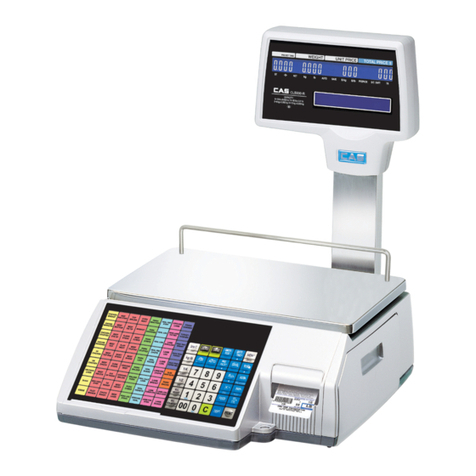
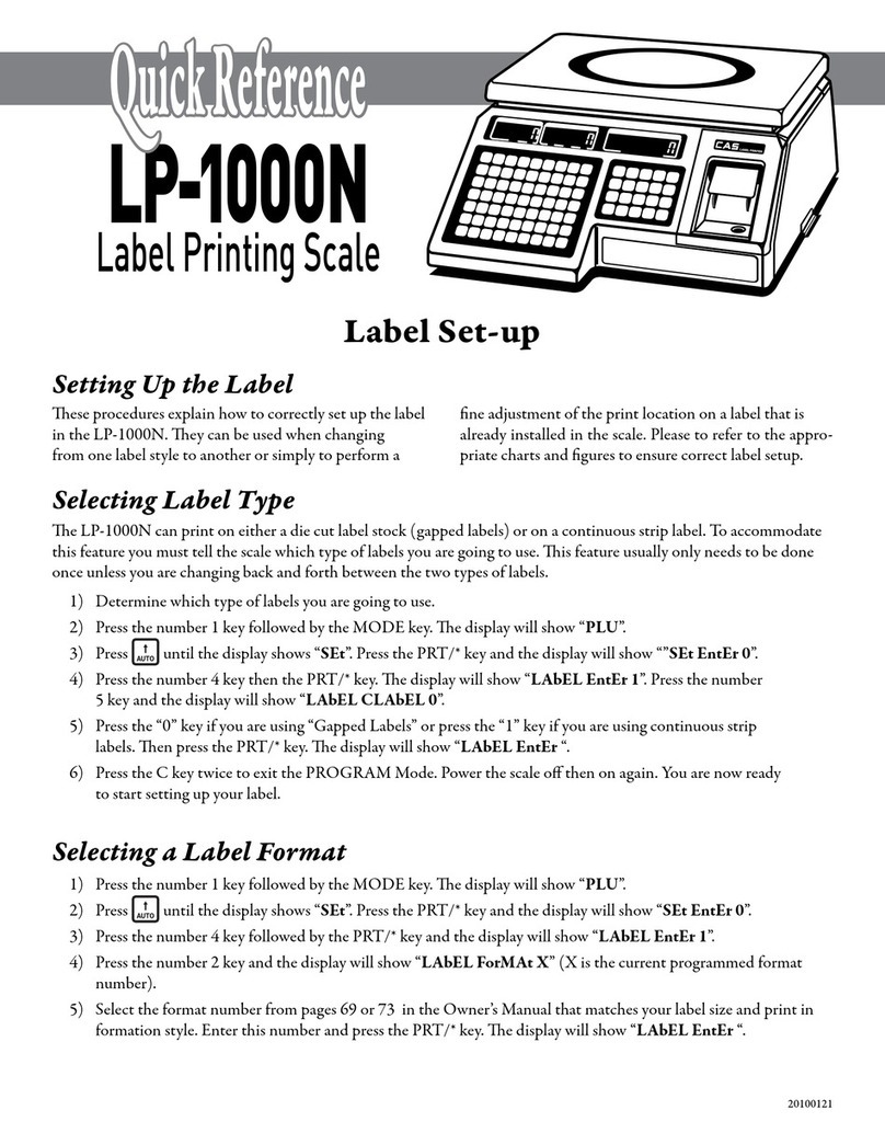
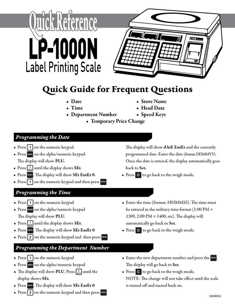
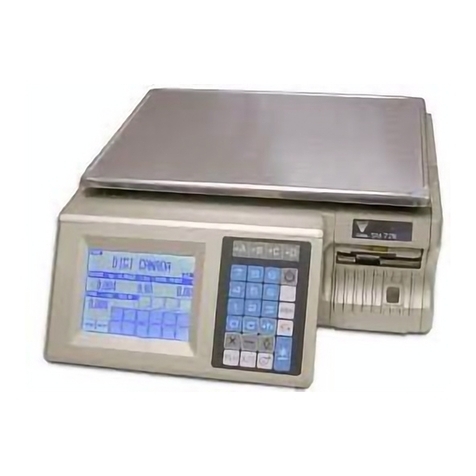
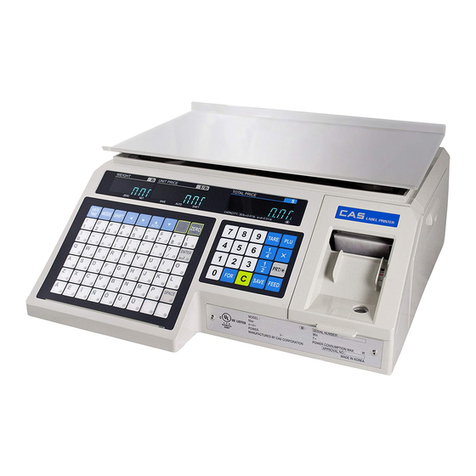
CAS Scale LP Series User manual

LP series
SERVICE MANUAL
( LP-1 ver 1.7 )
THERMAL LABEL PRINTING SCALE
S • C • A • L • E

INDEX
1. BLOCK DIAGRAM
2. CONNECTION DAIGRAM
3. OPENNING THE UNIT
4. SCALE CALIBRATION
5. SCHEMATIC DIAGRAM
6. PCB LAYOUT
7. TROUBLE SHOOTING FLOWCHART
8. PARTS LIST
9. EXPLODED VIEW – UPPER CASE
10. EXPLODED VIEW – BODY
11. SEALING METHOD
12. INTERFACE LIST
13. LOAD CELL DIAGRAM
14. SMPS SPECIFICATION
A. SAMIK(6190-PLP-0114-0)
B. FINE SUNTRONIX(6190-PLP-7040-0)

1. BLOCK DIAGRAM
Drawing No.: 9000-L17-0001-0
CPU
ATMEGA103
Display
Driver
Front/Rear
Display
TPH
Data
Flash
RTC
Battery 3.6V
Regulator
Step Motor
Driver
Stepping Motor
GAB
Sensor
Peel
Sensor
Headup
Sesor
KeyBoard
Mode
Switch
RS232C
Driver
Interface
Connector
ADC
Module Load Cell
CAL
Switch
Reset
IC
Buzzer
SMPS
AC 85V ~ 264V
220V/3.0A

2. CONNECTION DAIGRAM
Drawing No.: 9000-L17-0002-0
NOISE FILTER
CN1
CN24
CN21
J4
J10
J13(GAP)
J14(HEAD UP)
J8(PEEL LED)
J9(PEEL OPTO)
SENSOR
J7
J5
J11
J1
J6 J5
THERMAL
HEAD STEPPING
MOTOR
A/D
CONVERTER
6144-A00-0065-0
INTERFACE
CONNECTOR
25PIN
POWER
BOARD
6190-PLP-0114-0
(6190-PLP-7040-0) MAIN
BOARD
6191-PLP-0200-0
DISPLAY
BOARD
6110-PLP-0236-0
J6
J1
MEMBRANE
KEY, SMALL MEMBRANE
KEY, LARGE
J3
CN1
REAR
DISPLAY
6110-PLP-0234-0
(6156-PLP-0082-0) CN4CN2 CN3
POLE
DISPLAY
6110-PLP
-0316-0
AC 85~264V
220V/5.0A

3. OPENNING THE UNIT
A. Removing the Display PCB
i. Disconnect AC code.
ii. Put the scale where you can reach both the back and the front of
it easily.
iii. Refer to “12. EXPLODED VIEW – UPPER CASE.”
Pull out the tray and the paper cover.
iv. On the front side of the upper case are the four screws holding
the front cover on. Unscrew them and put them in a safe place
v. Unscrew a bolt that is on the left front side of the main body and
put it in a safe place.
vi. Lift the front cover and pull it. Carefully remove the all cables
including the FPC of the membrane key boards and unscrew the
screws fastened to the main body with the ground wires.
vii. The five screws are holding the main PCB on the front cover.
Remove them and place them in a safe place. Loosing the five
hooks, pull out the board.
B. Removing the Main PCB
i. Follow the steps 1) ~ 5) listed in “1. Removing the Display PCB”.
ii. Remove the platform, side cover, upper case and rear cover.
Refer to “12. EXPLODED VIEW – UPPER CASE.”
iii. Remove the all cables on Main board
iv. Refer to “13. EXPLODED VIEW – PRINTER MECHANISM.” Unscrew
the three screws fixing the printer on the main body. Remove the
sensor support from the main body.
v. Carefully pull out the printer.
vi. On the printer, the four screws holding the Main PCB. Unscrew
them and put them in a safe place.

4. SCALE CALIBRATION
A. Description
i. CAL#1 : Shows the span – adusted ADC output.
ii. CAL#2 : Key test mode
iii. CAL#3 : Span calibration is carried in the mode
iv. CAL#4 : Scale Setting mode
v. CAL#5 : Pure ADC output
vi. CAL#6 : Printer sensor setting
vii. CAL#8 : Display test
B. Calibration procedure
i. Turn the power switch off
ii. Remove the tray and slide the “CAL” switch toward the other side.
iii. Put the tray on the platform.
iv. Turn the power switch on.
v. CAL#4 Setting
vi. CAL#3 Span calibration
vii. CAL#1 Verification & Fine tuning

WEIGHT kg UNIT PRICE $/kg
CAL1 0 8594
It indicates the factored AD value.
In other words, it shows the
relative value that the first point of
time that you press zero key or
you enter the CAL1 mode
supposes zero point. Once you
press zero key and put up total
value of scale, 60000 value is
indicated.
It indicates the factored raw AD
value of scale.
CAL2 10
This item is used to test keys. The
indicated number 10 is the value
when you select key1 of PLU PAD.
Through this item, you can know
whether keys are faulty or not.
CAL3 UnLoAd
When you press the ‘C’ key, you can
leave
In case of pressing ‘PRT’ key at
‘Unload’
Ex) In case of 15kg scale
1. After checking nothing on the platter, press ‘PRT’ key.
2. When the ‘Load’ is indicated, put up 15kg weight and press ‘PRT’ key.
3. It is over, when you hear the sound and unit price screen is disappeared.
WEIGHT kg UNIT PRICE $/kg
CAL3 LoAd
WEIGHT kg UNIT PRICE $/kg

CAL4 0
It set the capacity of scale.
1: 6kg single 2. 6kg dual
3 : 15kg single 4. 15kg dual
5 : 30kg single 6. 30kg dual
CAL5 08594
It indicates raw AD value. In other
words, it shows the relative value
that the first point of time that you
press zero key or you enter the
CAL1 mode supposes zero point.
It indicates raw AD value of scale.
CAL6 CAL6 PRint
CAL6 tESt CHESS Press ‘PRT’key, the TEST CHESS label is issued.
CAL6 CAL SEnSor Press ‘PRT’ key, the gap and peel sensor is measured automatically.
CAL6 HEiGHt Press ‘PRT’ key and enter the height of paper.
CAL6 P-oFF Press ‘PRT’ key and enter whether using the peel sensor.
(1: use, 0: don’t use)
CAL6 intEnS Press ‘PRT’ key and enter the printing density. (0~4 step)
CAL6 AdJUSt Press ‘PRT’ key and adjust minutely the printing scope.
CAL6 Print PArAMEt Press ‘PRT’ key, the print setting is printed.
CAL6 SEt dEFAULt Press ‘PRT’ key, a print setting is set as default.
CAL6 SHoP PrE-Prt Press ‘PRT’ key and enter the height of printing scope.
(standard : 80) - In this case, 80 means 10mm.
CAL6 tESt CHESS
CAL7 P-nUM 100
You can set the all kind of setting values. It will be applied, if you enter the
appropriate number and modify the value. (Parameter Setting)
This mode is used to DISPLAY TEST
It is used to set whether the application of hysteresis
compensation.
WEIGHT kg UNIT PRICE $/kg
PRT/*
5. SCHEMATIC DIAGRAM
A. Main Board Schematic
(a) CPU and Memory Part (Document No: 9000-L17-0003)

(b) Power and I/O Part (Document No: 9000-L17-0004)

B. Display Board Schematic (Document No: 9000-L17-0005)

6. PCB DIAGRAM
A. Main PCB Diagram (PCB No.: 6191-PLP-0200-0)
(a) Top Part (Document No: 9000-L17-0006)

(b) Bottom Part (Document No: 9000-L17-0007)

B. Display PCB Diagram (PCB No.: 6110-PLP-0236-0)
(a) Top Part (Document No: 9000-L17-0008)

(b) Bottom Part (Document No: 9000-L17-0009)

7. TROUBLE SHOOTING FLOWCHART
Drawing No.: 9000-L17-0010-0

8. PARTS LIST
A. Main PCB
NO PARTS NAME SPECIFICATION UNIT Q'TY REMARK
1 PCB 6191-PLP-0200-0 6191-PLP-0200-0 1 PCB
2 IC(CPU) ATMEGA128 6200-IPU-0128-A 1 U7
3 IC(CPLD) M4A5-32/32-10VC 6216-IS0-0032-0 1 U8
4 IC(SRAM) LP621024D-70LL 6202-IS0-6810-0 1 U1
5 IC(FLASH MEMORY) SST39SF040-70-4C-WH 6204-IS0-3904-0 2 U5,6
6 IC(NV RAM CONTROL) DS1210S/bq2201 (SOIC) 6202-IS0-1210-0 1 U4
7 IC(TIMER) DS1302 6228-IS0-1302-0 1 U16
8 IC(DRIVER) TD62064BP-1 6224-I00-6264-0 1 U12
9 IC(C MOS) 74HC573 6236-IS0-0573-A 3 U2,13,14
10 IC(C MOS) 74HC245 6236-IS0-0245-A 2 U10,15
11 IC(C MOS) 74HC123 6236-IS0-0123-0 1 U11
12 IC(INTERFACE) SP232ECN(SIPEX) 6232-IS0-1232-0 1 U3
13 CRYSTAL 32.768KHz 7010-ZK0-3276-0 1 Y2
14 CRYSTAL 11.0592MHz 7010-ZM0-1105-A 1 Y1
15 IC(RESET) KIA7045AP/AF 6210-IS0-7045-0 1 U9
16 MOSFET SFP9530(IRF9530) 6273-I00-9530-0 1 Q1
17 TRANSISTOR CHIP KTC3875 6281-I00-3875-0 1 Q2
18 FERRITE BEAD SMD ARRAY MZA3216R102A(TDK) 6810-F00-0102-0 1 L1
19 RESISTOR-CHIP 1/10W RR1220P-331D 6527-ID0-3300-0 2 R7,26
20 RESISTOR-CHIP 1/10W RR1220P-102D 6527-ID3-0010-0 4 R1,3,6,16
21 RESISTOR-CHIP 1/10W RR1220P-104D 6527-ID3-1000-0 1 R10
22 RESISTOR-CHIP 1/10W RR1220P-103D 6527-ID3-0100-0 10 R8,9,12,15,17,20,
21,22,28,31
23 RESISTOR-CHIP 1/10W RR1220P-203D 6527-ID3-0200-0 3 R11,13,23
24 RESISTOR-CHIP 1/10W RR1220P-221D 6527-ID0-2200-0 3 R24,27,29
25 RESISTOR-CHIP 1/10W RR1220P-472D 6527-ID3-0047-0 6 R2,4,14,18,19,25
26 RESISTOR-CHIP 1/10W RR1220P-473D 6527-ID3-0470-0 1 R30
27 RESISTOR C.F.R 3W 0.1 6511-CJ0-0001-0 1 R5
28 RESISTOR-CHIP-ARRAY RP164P103J(=1608 10kΩ X 4PCS) 6598-IJ3-0100-0 4 RN5~8

29 RESISTOR-CHIP-ARRAY RP164P101J(=1608 100Ω X 4PCS) 6598-IJ0-1000-0 6 RN2,3,4,9,11,12
30 CONDENSER-CHIP CL21F 104 KBNC 6712-CHP-0104-0 25 C5,8~11,15~34
31 CONDENSER-CHIP 105(1uF 0805 type) 6712-CHP-0105-0 5 C1~4,7
32 CONDENSER-CHIP CL21B 102 KBNC 6712-CHP-0102-0 2 C6,14
33 CONDENSER-CHIP CL21C 200 JBNC(20PF) 6712-CHP-0200-0 2 C12,13
34 CONDENSER-ELECTRIC 1000uF/25V 6704-C25-1000-0 1 CE1
35 CONDENSER-ELECTRIC 470uF/50V 6704-C50-0470-0 1 CE2
36 CONDENSER-ELECTRIC 100uF/6.8V 6.3 6706-C68-0100-0 1 CE3
37 DIODE CHIP KDS 160 6294-ICP-0160-0 1 D1
38 SOCKET CONNECTOR 5332-10P 7813-C00-0010-0 1 J2
39 SOCKET CONNECTOR 5332-20P 7813-C00-0020-0 1 J6
40 SOCKET CONNECTOR 5332-26P 7813-C00-0026-0 1 J7
41 CONNECTOR(WAFER) LW0640-05 7801-CLW-0005-0 1 J11
42 CONNECTOR(WAFER) 5267-02 7805-CCN-6702-0 2 J8,9
43 CONNECTOR(WAFER) 5267-03 7805-CCN-6703-0 1 J14
44 CONNECTOR(WAFER) LW0640-03 7801-CLW-0003-0 1 J1
45 CONNECTOR(WAFER) 5267-04 7805-CCN-6704-0 1 J13
46 CONNECTOR(WAFER) 5267-06 7805-CCN-6706-0 1 J5
47 CONNECTOR(WAFER) 5267-08 7805-CCN-6708-0 1 J10
48 CONNECTOR(WAFER) 5267-15 7805-CCN-6715-0 1 J4
49 CONNECTOR 929400-40(MALE) 7810-C00-9294-0 1 J3
50 LED LAMP ø3-GREEN 7232-DG0-0003-A 1 LED1
51 TACT S/W 11902(DJTA-1102) 7600-STA-1902-0 1 SW1
52 BATTERY-NIMH GP80BVH3A2H 7520-P00-0060-0 1 BT1
B. Front PCB
NO PARTS NAME SPECIFICATION UNIT Q'TY REMARK
1 PCB 6100-PLP-0236-0 6100-PLP-0236-0 1 PCB
2 IC(FIP DRIVER) UPD 16310GF-3L9 6224-IS0-1631-0 1 U1
3 IC(CMOS) 74HC154D(LP-II) 6236-IS0-0154-0 1 U2
4 RESISTOR-CHIP-ARRAY RP164P101J(=1608 100Ω X 4PCS) 6598-IJ0-1000-0 3 RN1,RN2,RN4
5 RESISTOR-CHIP-ARRAY RP164P103J(=1608 10kΩ X 4PCS) 6598-IJ3-0100-0 2 RN3,RN5
6 RESISTOR-CHIP 1/10W RR1220P-103D 6527-ID3-0100-0 1 R1

7 CONDENSER-CHIP CL21F 104 KBNC 6712-CHP-0104-0 6 C1,C3,C14~C17
8 CONDENSER-ELECTRIC 470uF/25V 6704-C25-0470-0 1 C2
9 CONDENSER-CERAMIC 0.1uF/25V 6710-CAP-0104-0 1 C4
10 CONDENSER-CHIP CL21B 102 KBNC 6712-CHP-0102-0 8 C5 ~C12
11 CONDENSER-CHIP CL21C 200 JBNC(20PF) 6712-CHP-0200-0 1 C13
12 SOCKET CONNECTOR 5332-20P 7813-C00-0020-0 1 J1
13 CONNECTOR(WAFER) 5267-02 7805-CCN-6702-0 1 J2
14 SOCKET CONNECTOR 5332-34P 7813-C00-0034-0 1 J3
15 CONNECTOR(WAFER) 5267-08 7805-CCN-6708-0 1 J4
16 FPC-CONNECTOR FCZ254-16S 7807-CFP-0016-0 1 J5
17 FPC-CONNECTOR FCZ254-11S 7807-CFP-0011-0 1 J6
18 PIEZO BUZZER 23C2912(SL1I-12FsP) 7002-Z00-0110-0 1 BZ1
19 VFD(FIP) INB-12MM51T(삼성 12DI) 7202-D00-0051-0 1 VFD1
20 VFD(FIP) F-52B(7 DIGIT) 7202-D00-052B-0 1 VFD2
21 CUSHION-VFD 30*20*2t 2631-A00-0001-0 3 2T

9. EXPLODED VIEW
A. Upper Case (Drawing No.: 3003-LPR-0001-1)
This manual suits for next models
1
Table of contents
Other CAS Scale Scale manuals

CAS Scale
CAS Scale LP-1000N series User manual

CAS Scale
CAS Scale EC-II User manual

CAS Scale
CAS Scale AP Series User manual

CAS Scale
CAS Scale LP-1000 Series User manual

CAS Scale
CAS Scale LP-1000N series User manual

CAS Scale
CAS Scale CL5000-P User manual

CAS Scale
CAS Scale CL 5000 User manual

CAS Scale
CAS Scale ND 300 User manual

CAS Scale
CAS Scale LP-1000N series User manual