Denon DHT-S216 User manual

Service Manual
SOUND BAR
DHT-S216 Click here!
On-line service parts list
https://dmedia.soundunited.com/documents/details/26504
ONLINE PARTS LIST (P5)
WEB owner’s manual
NA: http://manuals.denon.com/DHTS216/NA/EN/index.php
EU: http://manuals.denon.com/DHTS216/EU/EN/index.php
AP: http://manuals.denon.com/DHTS216/AP/ZH/index.php
JP: http://manuals.denon.com/DHTS216/JP/JA/index.php
Upload is planned for the time of a future press release.
BEFORE SERVICING THIS UNIT
ELECTRICAL
MECHANICAL
REPAIR INFORMATION
UPDATING
Ver. 2
Condential
•Forpurposesofimprovement,specicationsanddesignaresubjecttochangewithoutnotice.
• Please use this service manual whenreferringtotheoperatinginstructionswithoutfail.
• Some illustrations usedinthisservicemanualareslightlydifferentfromtheactualproduct. Please refer to the MODIFICATION NOTICE.

BEFORE SERVICING THIS UNIT
SAFETY PRECAUTIONS
NOTE FOR SCHEMATIC DIAGRAM
HANDLING THE SEMICONDUCTOR AND OPTICS
ONLINE PARTS LIST
Accessing the Parts List
Searching Part Numbers or Ref. Numbers
NOTE FOR PARTS LIST
SERIAL NUMBER
Serial Number Organization
SKU Code of this Unit
POST-SERVICE PRECAUTIONS
Initializing this Unit
Before Servicing
This Unit Electrical Mechanical Repair Information Updating
2

The following items should be checked for continued protection of the customer and the service technician.
Leakage current check
Before returning the set to the customer, be sure to carry out either (1) a leakage current check or (2) a line to chassis resistance check. If the leakage current exceeds 0.5 milliamps, or if the resistance from
chassis to either side of the power cord is less than 460 kohms, the set is defective.
Be sure to test for leakage current with the AC plug in both polarities, in addition, when the set's power is in each state (on, off and standby mode), if applicable.
CAUTION Please heed the following cautions and instructions during servic-
ing and inspection.
◎ Heed the cautions!
Cautions which are delicate in particular for servicing are labeled on the cabinets, the parts and the
chassis, etc. Be sure to heed these cautions and the cautions described in the handling instructions.
◎ Cautions concerning electric shock!
(1) An AC voltage is impressed on this set, so if you touch internal metal parts when the set is energized,
you may get an electric shock. Avoid getting an electric shock, by using an isolating transformer and
wearing gloves when servicing while the set is energized, or by unplugging the power cord when
replacing parts, for example.
(2) There are high voltage parts inside. Handle with extra care when the set is energized.
◎ Caution concerning disassembly and assembly!
Through great care is taken when parts were manufactured from sheet metal, there may be burrs on the
edges of parts. The burrs could cause injury if ngers are moved across them in some rare cases. Wear
gloves to protect your hands.
◎ Use only designated parts!
The set's parts have specic safety properties (re resistance, voltage resistance, etc.). Be sure to use
parts which have the same properties for replacement. The burrs have the same properties. In particular,
for the important safety parts that are indicated by the z mark on schematic diagrams and parts lists,
be sure to use the designated parts.
◎ Be sure to mount parts and arrange the wires as they were originally placed!
For safety seasons, some parts use tapes, tubes or other insulating materials, and some parts are
mounted away from the surface of printed circuit boards. Care should also be taken with the positions
of the wires by arranging them and using clamps to keep them away from heating and high voltage
parts, so be sure to set everything back as it was originally placed.
◎ Make a safety check after servicing!
Check that all screws, parts and wires removed or disconnected when servicing have been put back
in their original positions, check that no serviced parts have deteriorated the area around. Then make
an insulation check on the external metal connectors and between the blades of the power plug. And
otherwise check that safety is ensured.
(Insulation check procedure)
Unplug the power cord from the power outlet, disconnect the antenna, plugs, etc., and on the power.
Using a 500V insulation resistance tester, check that the insulation resistance value between the inplug
and the externally exposed metal parts (antenna terminal, headphones terminal, input terminal, etc.) is
1M Ω or greater. If it is less, the set must be inspected and repaired.
Many of the electric and the structural parts used in the set have special safety properties. In most
cases these properties are difcult to distinguish by sight, and the use of replacement parts with higher
ratings (rated power and withstand voltage) does not necessarily guarantee that safety performance
will be preserved. Parts with safety properties are indicated as shown below on the wiring diagrams and
the parts list in this service manual. Be sure to replace them with the parts which have the designated
part number.
(1) Schematic diagrams Indicated by the z mark.
(2) Parts lists Indicated by the z mark.
The use of parts other than the designated parts could cause electric shocks, res or other dangerous
situations.
CAUTION Concerning important safety parts
SAFETY PRECAUTIONS
Before Servicing
This Unit Electrical Mechanical Repair Information Updating
3

WARNING:
Parts indicated by the z mark have critical characteristics. Use ONLY replacement parts recommended
by the manufacturer.
CAUTION:
Before returning the set to the customer, be sure to carry out either (1) a leakage current check or (2)
a line to chassis resistance check. If the leakage current exceeds 0.5 milliamps, or if the resistance from
chassis to either side of the power cord is less than 460 kohms, the set is defective.
WARNING:
DO NOT return the set to the customer unless the problem is identied and remedied.
NOTICE:
(1) ALL RESISTANCE VALUES IN OHM. k=1,000 OHM / M=1,000,000 OHM
(2) ALL CAPACITANCE VALUES ARE EXPRESSED IN MICRO FARAD, UNLESS OTHERWISE INDICATED. P
INDICATES MICRO-MICRO FARAD. N INDICATES NANO FARAD.
(3) EACH VOLTAGE AND CURRENT ARE MEASURED AT NO SIGNAL INPUT CONDITION.
(4) CIRCUIT AND PARTS ARE SUBJECT TO CHANGE WITHOUT PRIOR NOTICE.
Electrostatic breakdown of the semi-conductors or optical pickup may occur due to a potential differ-
ence caused by electrostatic charge during unpacking or repair work.
1. Ground for Human Body
Be sure to wear a grounding band (1 M ohm) that is properly grounded to remove any static electricity
that may be charged on the body.
2. Ground for Workbench
Be sure to place a conductive sheet or copper plate with proper grounding (1 M ohm) on the workbench
or other surface, where the semi-conductors are to be placed. Because the static electricity charge
on clothing will not escape through the body grounding band, be careful to avoid contacting semi-
conductors with your clothing
<Incorrect>
CBA
Grounding Band
Conductive Sheet or
Copper Plate
1MΩ
1MΩ
<Correct>
CBA
NOTE FOR SCHEMATIC DIAGRAM
HANDLING THE SEMICONDUCTOR AND OPTICS
Before Servicing
This Unit Electrical Mechanical Repair Information Updating
4

ONLINE PARTS LIST
Accessing the Parts List
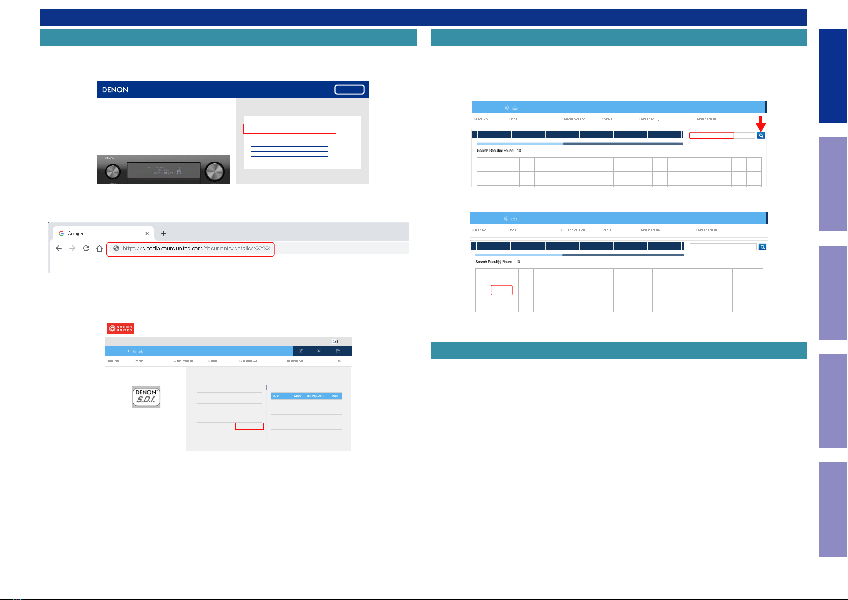
(1) Access from the Service Manual
・ Click the URL link on the cover of the service manual.
Examples of display
NOTE : If the web browser does not open automatically, copy the URL and paste it into the address bar
of the web browser and then press Enter.
(2) Accessing the Part List from the Model Asset Screen.
・ Display Model Asset from New SDI.
・ Click the section displayed as ▼ Link to Part Lists under the model name.
NOTE : If the ▼ Link to Parts List section is not displayed, download the parts table from the Asset list.
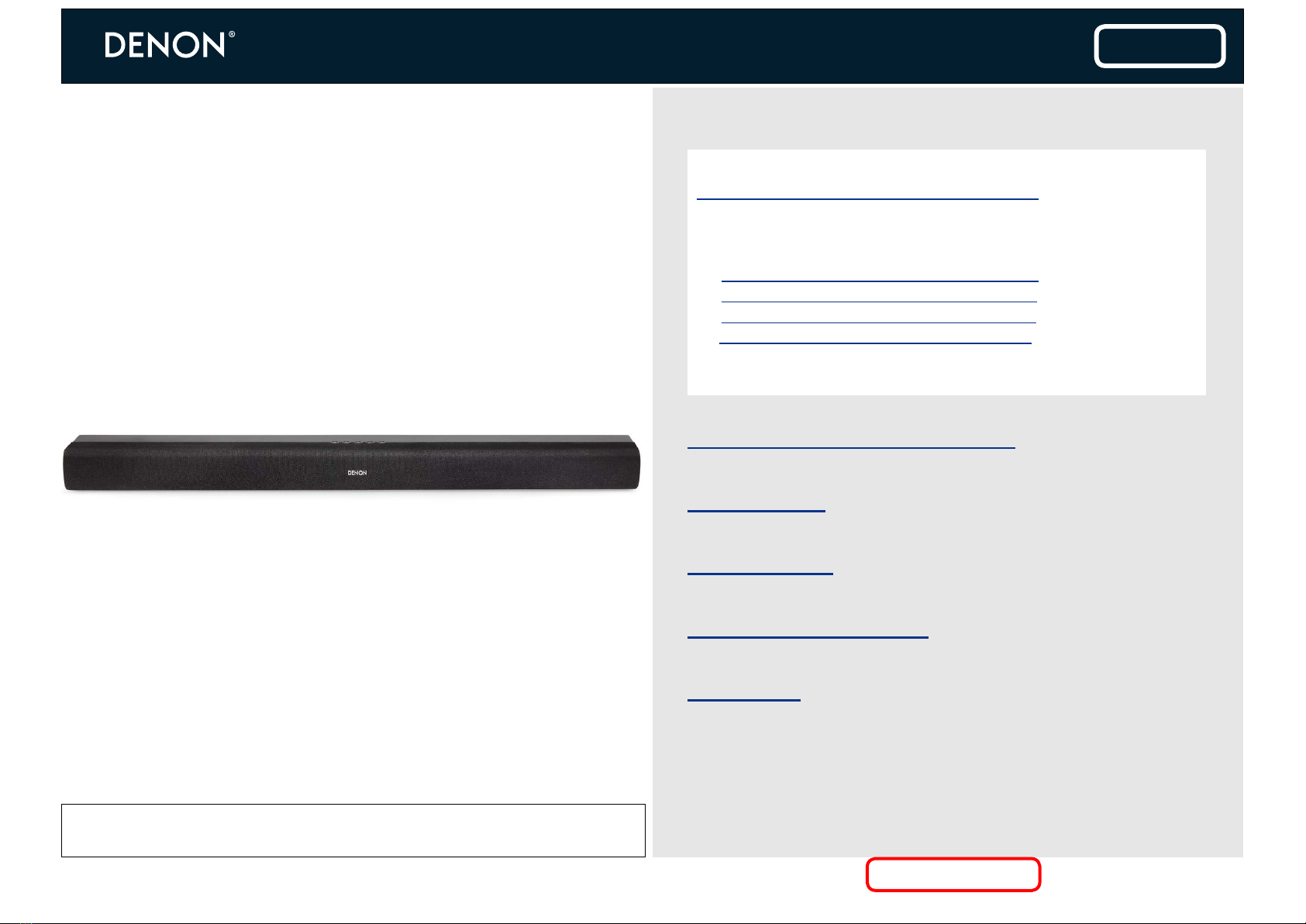
INTEGRATED NETWORK AV RECEIVER
AAA-AAAA
Service Manual
Click here!
On-line service parts list
https://dmedia.soundunited.com/documents/details/XXXXX
ONLINE PARTS LIST (P5)
WEB owner’s manual
NA: http://manuals.denon.com/AAAAAAA/NA/EN/index.php
EU: http://manuals.denon.com/AAAAAAA/EU/EN/index.php
AP: http://manuals.denon.com/AAAAAAA/AP/ZH/index.php
JP: http://manuals.denon.com/AAAAAAA/JP/JA/index.php
Upload is planned for the time of a future press release.
BEFORE SERVICING THIS UNIT
Ver. 1
All Assets Tasks Drafts Notifications Deactivated Archived Advanced Search Search Content
Search
0000 XxxxxXxxxx 32.2 Published XxxxxXxxxx 09-May-2019
A
sse
t
N
o
:
O
w
n
e
r
:
C
u
r
r
e
n
t
V
e
r
si
o
n
:
S
t
a
t
u
s:
P
u
b
l
i
sh
e
d
B
y:
P
u
b
l
i
sh
e
d
O
n
:
Bac
k
Additional Classification
Brand
Region AP - JAPAN, NA, E
U, AP - CHINA
Asset Type SDI
Category
XXXXXXXXXXXXXXXX
Description ▼Link to Parts List
XXXXXXXXXXXXXXXX
Version History
Version No. Type Created On
3
2
.
2
M
a
j
o
r
0
9
-
M
a
y
-
2
0
1
9
V
i
e
w
32.1 Major 23-Apr-2019 View
32.0 Major 07-Feb-2019 View
31.0 Major 07-Feb-2019 View
30.0 Major 24-Dec-2017 View
XXXXXXXXXX
(392.35 MB)
Download Pac kag
e
Edit Thi
s
Deactivat
e
Archi
ve
Denon
Searching Part Numbers or Ref. Numbers
You can search a Parts List for part numbers or Ref. numbers.
(1) Enter the part number or Ref. number in the search window of the Parts List, and press the search
button.
(2) The search results are displayed.
The name of the sheet in which the search part is used and the part’s line are displayed.
(3) Next, click the "Sheet" section of the search results.
Create Public URL
S
e
a
r
c
h
R
e
s
u
l
t
(
s
)
F
o
u
n
d
-
1
0
1SMPS D9001 943203500730S DIODE, RECTIFIER,
AXIAL CVD1N4007SL 1
2SMPS D9002 943203500730S DIODE, RECTIFIER,
AXIAL CVD1N4007SL 1
3SMPS D9003 943203500730S DIODE, RECTIFIER,
AXIAL CVD1N4007SL 1
4SMPS D9004 943203500730S DIODE, RECTIFIER,
AXIAL CVD1N4007SL 1
5SMPS D9005 943203500730S DIODE, RECTIFIER,
AXIAL CVD1N4007SL 1
6SMPS D9008 943203500730S DIODE, RECTIFIER,
AXIAL CVD1N4007SL 1
7FRONT D6005 943203500730S DIODE, RECTIFIER,
AXIAL CVD1N4007SL 1
8FRONT D6006 943203500730S DIODE, RECTIFIER,
AXIAL CVD1N4007SL 1
9FRONT D6007 943203500730S DIODE, RECTIFIER,
AXIAL CVD1N4007SL 1
10 FRONT D6018 943203500730S DIODE, RECTIFIER,
AXIAL CVD1N4007SL 1
FRONT INPUT VIDEO F.CNT S.CNT DIGITAL 943203500730S
21095 Super Administrator 1.2 Published Kazuhiro Nakai 23-Jul-2019
A
sse
t
N
o
:
O
w
n
e
r
:
C
u
r
r
e
n
t
V
e
r
si
o
n
:
S
t
a
t
u
s:
P
u
b
l
i
sh
e
d
B
y:
P
u
b
l
i
sh
e
d
O
n
:
SR6014 Parts List (525.24 KB)
Download Package
1. Parts indicated by "nsp" on this table cannot be supplied.
2. When ordering a part, make a clear distinction between "1" and "I" (i) to avoid mis-supplying.
3. A part ordered without specifying its part number can not be supplied.
4. Part indicated by "@" mark is not illustrated in the exploded and packaging view.
WARNING: Parts indicated by the z mark have critical characteristics. Use ONLY replacement parts
recommended by the manufacturer.
NOTE FOR PARTS LIST
Before Servicing
This Unit Electrical Mechanical Repair Information Updating
5

Product SKU SKU Code
DHTS216BKE3 DBBB
DHTS216BKE2 DBBC
DHTS216BKE1C DBBF
DHTS216K DBBD
SERIAL NUMBER
Serial Number Organization
The 14-digit serial number that contains the code of the manufacturing plant and the manufacturing
date.
Cumulative
serial number
SKU code Month
(01 ~ 12) The last
2digit of year
13 digits
SKU Code of this Unit
Before Servicing
This Unit Electrical Mechanical Repair Information Updating
6

Make sure to initialize this unit after replacing the microcomputer or any peripheral equipment, or the
PCB.
(1) While the power is On, hold down buttons "POWER", "SOURCE" and "VOL+" for at least 5 seconds.
(2) All LEDs light up three times after initialization.
LED1 LED2 LED3 LED4 LED5
Step 1 Red Red Red Red Off
Step 2 Red Red Red Red Off
Step 3 Red Red Red Red Off
(3) Wait six seconds before turning on the power again.
Initializing this Unit
POST-SERVICE PRECAUTIONS
Before Servicing
This Unit Electrical Mechanical Repair Information Updating
7

ELECTRICAL
SCHEMATIC DIAGRAMS
SCH01 MAIN 01
SCH02 MAIN 02
SCH03 MAIN 03
SCH04 MAIN 04
SCH05 MAIN 05
SCH06 MAIN 06
SCH07 MAIN 07
SCH08 MAIN 08
SCH09 MAIN 09
SCH10 MAIN 10
SCH11 BT 01
SCH12 BT 02
SCH13 POWER
PRINTED CIRCUIT BOARDS
MAIN, CD CONNECT, FRONT, LED, PSW, POWER
BLOCK DIAGRAM
POWER DIAGRAM
POWER DIAGRAM for STB MODE
WIRING DIAGRAM
Remote Code Table
Before Servicing
This Unit Electrical Mechanical Repair Information Updating
8

SCH01 MAIN 01
STB Mode ,OPWRSB=H GPIO4=H
Coreoff Mode ,OPWRSB=H GPIO4=L
DC-DC 20V-->STB_5V
EN: 1.3V<=EN<33V
Vout= 0.6*(R_1+R_2)/R_2
01UBUCK1-SY82132
Vin
:
4.5V<Vin<30V
5V /3A OUT
01UBUCK1-SY80881EN: 1.2V<=EN<6.6V
Vout= 0.6*(R_1+R_2)/R_2
Vin
:
2.5V<Vin<5.5V
5V IN 3.3V/1A OUT
R_2
R_1
3.3/5V IN
01UBUCK4-SY80881EN: 1.2V<=EN<6.6V
Vout= 0.6*(R_1+R_2)/R_2
Vin
:
2.5V<Vin<5.5V
1.2V/1A OUT
R_2
R_1
3.3/5V IN
01UBUCK4-SY80881
Description: NC devices are reserved for
improved dynamic response.This is a
standard circuit
EN: 1.2V<=EN<6.6V
Vout= 0.6*(R_1+R_2)/R_2
Vin
:
2.5V<Vin<5.5V
1.2V/1A OUT
R_2
R_1
Description: NC devices are reserved for
improved dynamic response.This is a
standard circuit
Description: NC devices are reserved for
improved dynamic response.This is a
standard circuit
GPIO4
EN2
OPWRSB
EN1
EN1
EN1EN2
EN1
STB_5V
STB_5V
STB_5V
STB_5V
1.2V
STB_5V 1.5V
STB_5V
STB_3V3
AMP_VCC
STB_5V
AMP_VCC
USB_5V
SYS_3V3
STB_3V3
GPIO4 [4]
OPWRSB [4]
SUB_FR+
[4]
SUB_FR- [4]
C17491000pF/50V/X7R
C113
300pF/50V/NP0
C1596
10UF/6.3V/X5R
C273
0.1uF/16V/X7R
C1591
NC/22pF/50V/NP0
C1731
NC/0.1uF/16V/X7R
R98 0Ω/0402
L44 2.2uH/2.1A
C1594
22pF/50V/NP0
C1593
10UF/6.3V/X5R
R11 0
Q614
3DG3904M
R1716
100K/1%
C1589
10UF/6.3V/X5R
R28 0
C1751
0.1uF/50V/X7R
R1714
100K/1%
R1878
56Ω
L45 2.2uH/2.1A
C1590
4.7UF/10V/X5R
L46 2.2uH/2.1A
C272
NC/0.1uF/16V/X7R
R1712
68K/1%
R2 0Ω
R1636
NC/1K
C9
0.1uF/50V/X5R
C14770.1uF/16V/X7R
R17 0
R793
47K
C44
NC/0.1uF/16V/X7R
C1729
NC/0.1uF/16V/X7R
R32
4.7K
C1714
0.1uF/50V/X7R
R1638
1K
C1
0.1uF/16V/X7R
R1735 0
R31
10K
R6
110K/1%
R1719
1K
C7
0.1uF/50V/X5R
Q615
3DG3904M
20V
C310uF/10V/X5R
R8
15K
C1730
NC/0.1uF/16V/X7R
C210uF/10V/X5R
C40
NC/0.1uF/16V/X7R
R30
4.7K
+
100uF/35VCE7
U1
SY8213FCC
BS 1
SS
4
LX 2
FB 5
VCC
6
EN
3
SVIN
7
PVIN
8
GND 9
R791
10K
R33
10K
R1877
56Ω
R1713
15K/1%
C17151000pF/50V/X7R
C8
1uF/10V/X5R
FB57 300/3A
C1750
0.1uF/50V/X7R
C1716
300pF/50V/NP0
C4
NC/4700pF/50V/X7R
R22 0
C1595
4.7UF/10V/X5R
C1588
NC/22pF/50V/NP0
R1 0Ω
C1592
4.7UF/10V/X5R
U613
SY8088
EN
1
VIN
4LX 3
VFB 5
GND
2
R1717
150K/1%
U612
SY8088
EN
1
VIN
4LX 3
VFB 5
GND
2
R14 0
R54.7Ω
C1713
0.1uF/50V/X5R
U614
SY8088
EN
1
VIN
4LX 3
VFB 5
GND
2
C17171000pF/50V/X7R
U608
JW7115-2
VIN
5
FLG 3
EN
4
VOUT 1
GND 2
R29
100K
C1476
0.1uF/16V/X7R
C1455 0.1uF/16V/X7R
R7
15K/1%
XP1
12P/2.0mm
12
3
4
5
6
78
910
12 11
L1 6.8uH/3A
C43
NC/22UF/6.3V/X5R
Q1
P_AP2305
G
DS
R1718
1K
Q2
3DG3904M
R49
10K
R3 0
R1715
100K/1%
C42
0.47uF/16V/X5R
R25 0
R4
100K
R792
4.7K
C51μF/50V/X7R
R34 4.7K
SCHEMATIC DIAGRAMS
Before Servicing
This Unit Electrical Mechanical Repair Information Updating
9

SCH02 MAIN 02
Close to IC
Close to IC
Close to IC
Close to IC
Close to IC
Close to IC
HDMI TX Port
Close to main IC
I2S DATA
ICE
AVDD33_PLLGP
NS_XTALI
NS_XTALO
VMID_PWMDAC
LRCK
SUB_DATA0
AMP_DATA0
BCLK
MCLK
AVDD12_HDMITX_C
AVDD33_HDMI
AVDD33_DACAVDD33_DAC
AVDD33_VDAC_X
AVDD12_HDMITX_D
AVDD12_HDMI_0_RX
AVDD33_DACAVDD33_DACAVDD33_DACAVDD33_DACAVDD33_DACAVDD33_DACAVDD33_DACAVDD33_DACAVDD33_DACAVDD33_DACAVDD33_DACAVDD33_DACAVDD33_DACAVDD33_DACAVDD33_DACAVDD33_DACAVDD33_DACAVDD33_DACAVDD33_DACAVDD33_DAC
AVDD33_VDAC_R
NS_XTALI
NS_XTALO
AVDD33_HDMI_0_RX
SUB_DATA0
AMP_DATA0
ADC_MCLK
BCLK
LRCK
ADC_LRCK
ADC_BCLK
MCLK
AMP_MCLK
SUB_MCLK
AMP_BCLK
SUB_BCLK
AMP_LRCK
SUB_LRCK
TRST#
TDO
TCK
TMS
TDI
TMS
TCK
TDO
TDI
AMP_RST
AMP_MUTE
4558_PON
AMP_RST
AMP_MUTE
4558_PON
HD_RSTb
HD_RSTb
STB_3V3
SYS_3V3
SYS_3V3
1.2VSYS_3V3
SYS_3V3
SYS_3V3
STB_3V3
SYS_3V3
SUB_DATA0
AMP_DATA0
ADC_LRCK
ADC_BCLK
AMP_MCLK
AMP_BCLK 9
AMP_LRCK 9
ADC_MCLK
SUB_MCLK
SUB_BCLK
SUB_LRCK 9
AMP_RST
AMP_MUTE
4558_PON
HD_RSTb
R83 0
C197
1μF/10V
C33
27pF/50V/NP0
27pF/50V/NP0
R159610K
R1854 0
C196
NC/4.7uF/6.3V/X5R
TP644
C16
10pF/50V/NP0
R1864
NC/10K
TP631
TP25
C195
NC/0.1uF/16V/X7R
TP77
27MHz/10PPM
Y2
2
3
4
1
R55
33
R92
10K
TP629
C1456
22pF/50V/NP0
C83
4.7UF/6.3V/X5R
R37
10Ω
R1857 0
R1860 0
U6B
MT8502_PBGA_A_13 X 13
AVDD33_X A7
AVDD33_R A6
AVDD33_PLLGP
E1
AVSS33_PLLGP
E3
AVDD33_DAC
A2
AVSS33_DAC
B3
NS_XTALI
F3
NS_XTALO
F2
AL0
B4 AR0
A3
AOLRCK
C3 AOSDATA0
C2 AOSDATA1
D3 AOSDATA2
D2 AOSDATA3
D1
SPDIF B1
SPDIF_IN0 B2
SPDIF_IN1 A1
RSRV_06 C5
RSRV_05 C4
RSRV_04 B6
RSRV_03 B5
AVDD12_HDMITX_C A12
AVDD12_HDMITX_D C11
AVDD33_HDMI
A13
CH0_M B10
CH0_P A10
CH1_M B9
CH1_P A9
CH2_M B8
CH2_P A8
CLK_M B11
CLK_P A11
RSRV_01 E9
HTPLG D10
CEC F9
HDMISD C9
HDMISCK D9
VMID_PWMDAC
A4
HDMI_0_RX_2B
A14
HDMI_0_RX_2
B14
HDMI_0_RX_1B
A15
HDMI_0_RX_1
B15
HDMI_0_RX_0B
A16
HDMI_0_RX_0
B16
HDMI_0_RX_CB
A17
HDMI_0_RX_C
B17
HDMI_SDA_RX
A18
HDMI_SCL_RX
B18
HDMI_CEC_RX
C17
HDMI_HPD_CBUS_RX
C18
MHL_SENCE
C14
AVDD33_HDMI_0_RX
B13 AVDD12_HDMI_0_RX B12
RSRV_02 G9
C65
1uF/10V/X5R
R1867
10K
R1892
NC/10K
TP628
R63
33
R186510K
R861
10K
C66
0.1uF/16V/X7R
R1863 0
TP643
R284 0
R1856 0
TP645
C198
0.1uF/16V/X7R
C17
33pF/50V/NP0
33pF/50V/NP0
C194
0.1uF/16V/X7R
R81 0
C201
0.1uF/16V/X7R
TP630
R89 0
C465
NC/0.1uF/16V/X7R
R112
4.7K
R9410K
C460
1μF/10V
R107
0
R9910K
R1855 0
C1457
22pF/50V/NP0
R1861 0
R1891 0
R35
1M
TP627
R51
33
Before Servicing
This Unit Electrical Mechanical Repair Information Updating
10

SCH03 MAIN 03
HDMI Tx Port
2016-12-22 Add
HDMI Rx Port1
TX_ARC-
TX_HPD
TX_ARC-
TX_ARC+
HDMI_SDA
TX_CEC
HDMI_SCL
HDMI_VCC
HDMI_SDA
HDMI_SCL
TX_ARC+
HDMI_SDATX_CEC HDMI_SCL
HDMI_RX11-
HPD1
PWR5V_RX1
RXHPD1
RX1_CEC
PWR5V_RX1
RX1_SCL
RX1_SDA
HDMI_RXC1-
HDMI_RX01+
HDMI_RX01-
HDMI_RXC1+
HDMI_RX21-
HDMI_RX11+
HDMI_RX21+
RX1_SDA
RX1_SCL
RX1_CEC RX1_SCLRX1_SDA
HDMI_VCC
PWR5V_RX1
STB_5V HDMI_VCC
TX_ARC+
2
TX_ARC-2
TX_SDA2
TX_SCL2
TX_HPD2TX_CEC2
RX1_CEC2
RX01_SCL
2
RX01_SDA2
RXHPD1
2
RX21P 2
RX21M 2
RX11P 2
RX11M 2
RX01P 2
RX01M 2
RXC1P 2
RXC1M 2
PWR5V_RX01 2
TX1P
2
TX2M2
TX2P2
TX0P2
TX0M2
TX1M
2
TXCM2
TXCP2
ESD22
NC/ESD0402
2 1
C160
0.1uF/16V/X7R
ESD3NC/ESD0402
2 1
R1629 33
R241 NC/33
R258 1K
PBZ3
GND 1
GND 2
C212NC/22pF/50V/NP0
C159
22pF/50V/NP0
J3
HDMI JACK
1
2
3
4
5
6
7
8
9
10
11
12
13
14
15
16
17
18
19
2221
20 23
24
25
26
D7
1N4148WS
R1845
330K
ESD7
NC/ESD0402
2 1
R261 0Ω/0402
R236 33
R248
47K
C211
NC/22pF/50V/NP0
ESD10
NC/ESD0402
2 1
C210NC/22pF/50V/NP0
ESD8
NC/ESD0402
2 1
R1630
2K
J2
HDMI JACK
1
2
3
4
5
6
7
8
9
10
11
12
13
14
15
16
17
18
19
2221
20 23
24
25
26
ESD21NC/ESD0402
2 1
ESD6
NC/ESD0402
21
R260
10K
R235 33
R1628 33
PBZ2
GND 1
GND 2
R1846 180KΩ
C158
22pF/50V/NP0
D5
1N4148WS
R243 1
R256
100K
Q9
P_AP2309
G
DS
R249
47K
ESD9
NC/ESD0402
2 1
R1631
2K
R242
47K
Before Servicing
This Unit Electrical Mechanical Repair Information Updating
11

SCH04 MAIN 04
Close to DRAM
For DDRVCCIO
close to DRAM
For UD1
Core Power
Close to Main IC
Close pin
Close pin
Differential Clock
DRAM Ref Volt.
Close pin
DDR3#1
RCLK0
RCLK0_
DDR_VREF3
DDR_VREF1
DDRVREF
ARTN
ARTP
MEM_TN
MEM_TP
AVDD12_DDRAVDD33_DDR
AVDD33_DDR
AVDD12_DDR
RCAS_
RA7
RA12
RA3
RCKE
RBA2
RWE_
RA4
RA9
RA13
RBA1
RA2
RA11
RCS_
RA6
RA8
RA5
RRAS_
RODT
RRESET
RA0
RA10
RA1
RBA0
RCSX_
RCLK0
RCLK0_
RDQ6
RDQ8
RDQ10
RDQ11
RDQ3
RDQ13
RDQ12
RDQ15
RDQ14
RDQ7
RDQ5
RDQ1
RDQ4
RDQ9
RDQ0
RDQ2
RDQM1
RDQM0
RDQS1_
RDQS0_
RDQS1
RDQS0
ARTP
ARTN
MEM_TP
MEM_TN
DDRVCCIO_CK
DDRVCCIO_CK
DDRVREF
RA3_1
RBA0_1
RA2_1
RA5_1
RA13
RA9 RA9_1
RRESET_1
RA7_1
RA13_1
RA4
RA6
RBA1
RRAS_
RCKE
RODT
RCS_
RBA2
RA0
RRESET
RA7
RA3
RBA0
RA0_1
RBA2_1
RCS_1
RODT_1
RCKE_1
RA1 RA4_1
RA6_1
RA1_1
RA14
RA12
RA8
RA11
RA14_1
RA12_1
RA8_1
RA11_1
RCAS_
RWE_
RBA1_1
RRAS_1
RCAS_1
RWE_1
RA2
RA5
RA14
RA0_1
RA1_1
RA2_1
RA3_1
RA4_1
RA5_1
RA6_1
RA7_1
RA8_1
RA9_1
RA10_1
RA11_1
RA12_1
RDQ8
RDQ15
RDQ11
RDQ6
RDQ9
RDQ4
RDQ0
RDQ7
RDQ1
RCKE_1
RDQ14
RDQ12
RDQ2
RDQ5
RA14_1
DDR_VREF1
RDQ3
RBA2_1
RRESET_1
DDR_VREF3
RDQ10
RRAS_1
RDQS1_
RDQS0_
RDQS1
RDQM0
RDQM1
RDQS0
RCLK0
RCLK0_
E1_ZQ RCAS_1
RBA1_1
RCS_1
RBA0_1
RODT_1
RWE_1
RA13_1
RA10 RA10_1
RDQ13
DDRVREF
1.5V
1.5V
1.5V
1.2V
1.2VSYS_3V3 AVDD33_DDR AVDD12_DDR
1.2V
1.5V
1.5V1.2V
1.5V
C38
0.1uF/16V/X7R
TPD11
TPD24
TP11
RD1 0
C58
0.1uF/16V/X7R
R61 75
TPD5
C56
0.1uF/16V/X7R
C57
0.1uF/16V/X7R
TPD19
R78 0
TPD25
C62
0.1uF/16V/X7R
TPD13
R73
49.9,1%,NC
TPD9
C51
0.1uF/16V/X7R
CD1
1μF/10V
R72
48.7Ω/1%
C54
0.1uF/16V/X7R
TPD3
TPD8
C23
0.1uF/16V/X7R
R65
1K/1%
C27
0.1uF/16V/X7R
TPD22
R75 75
C53
0.1uF/16V/X7R
TPD27
RN2
75R*4
1
2
3
4
6
5
8
7
C24
0.1uF/16V/X7R
TPD10
C147
10UF/6.3V/X5R
TPD18
R74 75
C37
0.1uF/16V/X7R
C25
0.1uF/16V/X7R
TPD21
TPD2
C59
0.1uF/16V/X7R
C22
0.1uF/16V/X7R
C36
0.1uF/16V/X7R
RN4
75R*4
1
2
3
4
6
5
8
7
C60
0.1uF/16V/X7R
RN5
75R*4
1
2
3
4
6
5
8
7
RN3
75R*4
1
2
3
4
6
5
8
7
TPD12
RN1
75R*4
1
2
3
4
6
5
8
7
C130
1μF/6.3V/X7R
C28
0.1uF/16V/X7R
TPD23
R58
240
TPD17
C129
10UF/6.3V/X5R
R77 0
R67
100/1%
R66 0
C61
0.1uF/16V/X7R
C133
1μF/10V
R71
49.9,1%,NC
C52
0.1uF/16V/X7R
C20
0.1uF/16V/X7R
R76 75
C26
0.1uF/16V/X7R
TPD26
TPD6
TPD15
R68 75
C48
0.1uF/16V/X7R
TPD7
R62
1K/1%
TPD16
R64 75
C63
0.1uF/16V/X7R
C49
0.1uF/16V/X7R
TPD4
R70
120/1%
TPD1
TPD20
U6A
MT8502_PBGA_A_13 X 13
RDQ0 U6
RDQ1 U8
RDQ2 T6
RDQ3 T8
RDQ4 V5
RDQ5 U10
RDQ6 U5
RDQ7 T10
RDQ8 W10
RDQ9 Y4
RDQ10 W11
RDQ11 W4
RDQ12 W9
RDQ13 Y5
RDQ14 Y10
RDQ15 W5
RDQM0 V7
RDQM1 W6
RDQS0 W7
RDQS0_ Y7
RDQS1 Y8
RDQS1_ W8
RCSX_ U14
RODT T12
RCAS_ Y19
RRAS_ Y18
RCS_ T13
RWE_ V18
RCKE U12
RRESET Y20
RBA0 U20
RBA1 V17
RBA2 T15
RA0 U16
RA1 V14
RA2 V19
RA3 U19
RA4 W14
RA5 V20
RA6 Y15
RA7 W19
RA8 W15
RA9 U18
RA10 W13
RA11 Y16
RA12 W17
RA13 T17
RA14 V16
RCLK0 W12
RCLK0_ Y12
DDRVREF P11
AVDD33_DDR R20
AVSS33_DDR R19
AVDD12_DDR T20
DGND12_K
J9
DGND12_K
J10
DGND12_K
J11
DGND12_K
K9
DGND12_K
K10
DGND12_K
K11
DGND12_K
K12
DGND12_K
L9
DGND12_K
L10
DGND12_K
L11
DGND12_K
L12
DGND12_K
M9
DGND12_K
M10
DGND12_K
M11
DGND12_K
R11
DGND12_K
V6
DGND12_K
V9
DGND12_K
V13
DGND12_K
Y3
DGND12_K
Y11
DGND12_K
Y13
ARTP N12
ARTN N13
MEM_TP P13
MEM_TN P14
DVCC12_K
L7
DVCC12_K
M7
DVCC12_K
N7
DVCC12_K
M6
DVCC12_K
N6
DVCC12_K
N4
DVCC12_K
R4 DVCC12_K
P4
DVCC12_K
T3
DDRVCCIO P6
DDRVCCIO R5
DDRVCCIO U3
DDRVCCIO T5
DDRVCCIO V3
DDRVCCIO Y2
DDRVCCIO T4
DDRVCCIO W2
DDRVCCIO V2
DVCC12_K
V1
DGND12_K
R18
DGND12_K
W16
DGND12_K
W18
DGND12_K
W20
DVCC12_K
H8
DVCC12_K
J8
DVCC12_K
K8
DVCC12_K
L8
DVCC12_K
M8
DVCC12_K
M5
DVCC12_K
M4
DVCC12_K
W1
DGND12_K
B7
DGND12_K
B19
DGND12_K
C6
DGND12_K
C12
DGND12_K
D11
DGND12_K
D12
DGND12_K
G16
DGND12_K
G17
DGND12_K
H15
DVCC12_K
U2
DVCC12_K
P5 DVCC12_K
N5
DVCC12_K
H9
DGND12_k
D4
DGND12_k
D5
DGND12_k
D6
DGND12_K
E5
DGND12_K
E6
DGND12_K
E10
DGND12_K
E11
DGND12_K
E12
DGND12_K
F5
DGND12_K
F6
DGND12_K
F10
DGND12_K
F11
DGND12_K
F12
DGND12_K
F13
DGND12_K
F15
DGND12_K
G10
DGND12_K
G11
DGND12_K
G12
DGND12_K
G13
DGND12_K
G14
DGND12_K
H10
DGND12_K
H11
DGND12_K
H12
DGND12_K
J12
DGND12_K
J13
DGND12_K
K13
DGND12_K
L13
DGND12_K
N8
DGND12_K
N9
DGND12_K
N10
DGND12_K
N14
DGND12_K
N15
DGND12_K
N16
DGND12_K
P8
DGND12_K
P9
DGND12_K
P10
DGND12_K
P16
DGND12_K
P17
DGND12_K
P18
DGND12_K
R8
DGND12_K
R17
DGND12_K
Y1
DDRVCCIO_CK W3
UD1
DDR3-16bit-FBGA96 1Gbits
VDD_0
B2
NC_0 J1
VSS_0 A9
VSSQ_0 B1
UDQS#
B7
VDDQ_0
A1
DQ14
B8
VSSQ_1 B9
UDM
D3
UDQS
C7
VSSQ_2 D1
DQ15
A3
VDDQ_1
A8
DQ9
C3
VDDQ_2
C1
VDDQ_3
C9
DQ8
D7
VDDQ_4
D2
DQ12
A7
VSSQ_3 D8
DQ11
C2 DQ10
C8
VSSQ_4 E2
DQ13
A2
VDD_1
D9
NC_1 J9
VSS_1 B3
VSSQ_5 E8
LDQS#
G3
VDDQ_5
E9
DQ6
G2
VSSQ_6 F9
LDM
E7
LDQS
F3
VSSQ_7 G1
DQ7
H7
VDDQ_6
F1
DQ1
F7
VDDQ_7
H2
DQ0
E3
VDDQ_8
H9
DQ4
H3
VSSQ_8 G9
DQ3
F8 DQ2
F2
BA2 M3
DQ5
H8
VDD_5
N1
VREFDQ
H1
VSS_2 E1
VSS_5 J8
CK J7
VDD_2
G7
CKE K9
WE# L3
RAS# J3
CK# K7
ODT K1
RESET#
T2
BA0 M2
BA1 N8
CAS# K3
CS# L2
A10/AP L7
A1 P7
A2 P3
A0 N3
VDD_3
K2 VSS_3 G8
A3 N2
A5 P2
A6 R8
A4 P8
A7 R2
A9 R3
A11 R7
A8 T8
VSS_4 J2
VDD_4
K8
A12/BC# N7
NC_3 L9
ZQ
L8
NC_2 L1
VREFCA
M8
NC_4 M7
NC_5 T3
NC_6 T7
VSS_6 M1
VSS_7 M9
VSS_8 P1
VSS_9 P9
VSS_10 T1
VSS_11 T9
VDD_6
N9
VDD_7
R1 VDD_8
R9
C50
0.1uF/16V/X7R
TPD28
Before Servicing
This Unit Electrical Mechanical Repair Information Updating
12

ES7241(Slave)
,
MT8502(Master)
Audio inPUT
ADC_BCLK
ADC_MCLK
ADC_LRCK
ADC_DATA
AUX_R
AUX_L
AUX_R
AUX_L
ADC_MCLK
ADC_BCLK
ADC_LRCK
ADC_DATA
ADC_RST
SYS_3V3
SYS_3V3
A
A
A
A
SYS_3V3
A
A
A
A
ADC_RST
ADC_MCLK
ADC_BCLK
ADC_LRCK
ADC_DATA
ADC_RST
U11
ES7241
VDDP
1
SDOUT
2
PAD
17
VDDD
4
SCLK
5
LRCK
6
RESETb
7
AINL 8
REFQ 9
AINR 10
VDDA 11
GNDA 12
REFP 13
M1
14 M0
15
MCLK
16
GNDD
3
R296 1K
C320
NC/10UF/6.3V
R295
4.7
R1639 7.5K/1%
ESD23NC/ESD0402
2 1
R252 10K
C959
100pF/50V/NP0
R304 0
R299 33
C67
180pF/50V/NP0
R297 33
C64 1uF/10V/X5R
C1637
10pF/50V/NP0
R1021 0
C1712
100uF/6.3V/X5R
C317
10UF/6.3V/X5R
R305 0
C1635
10pF/50V/NP0
R303 10K
C85 0.1uF/16V/X7R
R13310K/1%
P3
5PIN/CKX-3.5-29
M1 M1
M3 M3
M4 M4
M5 M5
M6 M6
R253
10K
C319
0.1uF/16V/X7R
R13410K/1%
C316
0.1uF/16V/X7R
C958
100pF/50V/NP0
R1640 7.5K/1%
C74
180pF/50V/NP0
ESD24
NC/ESD0402
2 1
R298 33
C55 1uF/10V/X5R
C318
10UF/6.3V/X5R
C1636
10pF/50V/NP0
R251 33
R302 10K
C1634
10pF/50V/NP0
C76 0.1uF/16V/X7R
SCH05 MAIN 05
Before Servicing
This Unit Electrical Mechanical Repair Information Updating
13

AMP_SCL
AMP_SDA
AMP_RST
AMP_DATA0
AMP_LRCK
AMP_MCLK
AMP_BCLK
AMP_FAULT
AMP_MUTE
AMP_SDA
MID_L-
AMP_FAULT
A_MUTE
AMP_RST
AMP_MCLK
AMP_BCLK
AMP_LRCK
AMP_DATA0
MID_L+
AMP_SCL
MID_R+
MID_R-
MID_L+
MID_L-
AMP_FAULT
A_MUTE
AMP_MUTE
MID_R+
TW_R+
MID_R-
TW_R-
MID_L+
TW_L+
MID_L-
TW_L-
MID_R+
MID_R-
TW_R+
TW_R-
MID_L+
MID_L-
TW_L+
TW_L-
A_MUTE
+3.3VD
AMP_20V
+3.3VD
+3.3VD
+3.3VD
AMP_20V
AMP_VCC
SYS_3V3 +3.3VD
+3.3VD
AMP_VCC
+3.3VD
AMP_SCL
AMP_SDA
AMP_RST
AMP_DATA0
AMP_LRCK
AMP_MCLK
AMP_BCLK
AMP_FAULT
AMP_MUTE
A_MUTE
C1718
NC/0.1uF/50V/X7R
C123
0.1uF/50V/X7R
C140
0.1uF/50V/X7R
C144
4700pF/50V/X7R
C1722 100pF/50V/NP0
C362
2.2uF/100V
C1641
1μF
R1787 2.2
R169 6.2
C1693
2.2uF/100V
C1380.1uF/50V/X7R
C69
10pF/50V/NP0
C687
100pF/50V/NP0
R214 NC/33
Q25
NPN_3DG3904M
Q23
PNP_3CG3906M
C97610pF/50V/NP0
XP15
4PIN/2.0mm
1
1
2
2
3
3
4
4
R177 0
R1900
NC/6.2
R997
2K
C685
100pF/50V/NP0
L54 10uH/5A
C927
0.47UF
C1746 NC/0.1uF/50V/X7R
R1014
100
Q622
NPN_3DG3904M
Q8
PNP_3CG3906M
R1790 47K
XP16
5PIN/1.0mm
1
1
2
2
3
3
4
4
5
5
R173 0
R1015
100K
C128
0.01UF/100V
R1785
4.7K
C1703
1μF
R1899
NC/6.2
C1696
100pF/50V/NP0
C1694
100pF/50V/NP0
L52 10uH/5A
C965
10uF/16V/X5R
C121
330pF/50V/X7R
C132
330pF/50V/X7R
R1783
NC/4.7K
FB32 500Ω/800mA
C97810pF/50V/NP0
R198 33
C963
10UF/6.3V/X5R
FB53 300/3A
C1640
10pF/50V/NP0
R1013
220K
C126
0.1uF/50V/X7R
R175 6.2
R1788 33
C1745 1000pF/50V/X7R
+
220uF/35V
CE282
C1744 1000pF/50V/X7R
R1898
NC/6.2
L15 10uH/5A
C1732 100pF/50V/NP0
R1011 220K
R165 6.2
R174
22
R1874 4.7K
C980
10pF/50V/NP0
C134
0.01UF/100V
U14
STA339BW
GND_SUB 1
SA 2
TEST_MODE 3
VSS 4
VCC_REG 5
OUT2B 6
GND2 7
VCC2 8
OUT2A 9
OUT1B 10
VCC1 11
GND1 12
OUT1A 13
GND_REG 14
VDD 15
CONFIG 16
OUT3B / FFX3B 17
OUT3A / FFX3A 18
EAPD / OUT4B
19
TWARN / OUT4A
20
VDD_DIG
21
GND_DIG
22
PWRDN
23
VDD_PLL
24
FILTER_PLL
25
GND_PLL
26
XTI
27
BICKI
28
LRCKI
29
SDI
30
RESET
31
INT_LINE
32
SDA
33
SCL
34
GND_DIG
35
VDD_DIG
36
GND
37
C1723100pF/50V/NP0
C964
10UF/6.3V/X5R
C145
0.1uF/50V/X7R
C1642
0.1uF/50V/X7R
R1009 220K
R176
2.2K
C124 0.1uF/50V/X7R
R171 6.2
C97910pF/50V/NP0
D41 1N4148WS
C143
680pF/50V/X7R
C1390.1uF/50V/X7R
C688
100pF/50V/NP0
R1902 0Ω
R1786 33
C1350.1uF/50V/X7R
C1645
1000pF/50V/X7R
C1748 NC/0.1uF/50V/X7R
C1719
NC/0.1uF/50V/X7R
C686
100pF/50V/NP0
C1743 1000pF/50V/X7R
R1901 0Ω
C141 0.1uF/50V/X7R
C928
0.47UF
R159 4.7K
R161 10K
R996
5.6K
+
CE13
47uF/16V/SMD
C1740 1000pF/50V/X7R
C1752
0.1uF/50V/X7R
C1742 1000pF/50V/X7R
D6
1N4148WS
TP42
C1747 NC/0.1uF/50V/X7R
C1697
100pF/50V/NP0
C1180.1uF/50V/X7R
C1727
NC/0.1uF/50V/X7R
R160 47K
R1903 0Ω
R119 33
R1784
NC/4.7K
C1695
100pF/50V/NP0
TP44
C1643 0.1uF/50V/X7R
C142 0.1uF/50V/X7R
C163910pF/50V/NP0
C207
0.1uF/16V/X7R
R164 33
R1789 100 L53 10uH/5A
R191 33
C1733 100pF/50V/NP0
R1012 220K
R168
22
C136
0.1uF/50V/X7R
C1728
0.1uF/50V/X7R
C120
1000pF/50V/X7R
C97710pF/50V/NP0
C966
0.1uF/50V/X7R
C125 1000pF/50V/X7R
C1741 1000pF/50V/X7R
C1370.1uF/50V/X7R
FB52 300/3A
C146
1000pF/50V/X7R
C1734 1000pF/50V/X7R
Q24
PNP_3CG3906M
R1010 220K
R91
NC/4.7K
C122
0.1uF/50V/X7R
C131 0.1uF/50V/X7R
SCH06 MAIN 06
Before Servicing
This Unit Electrical Mechanical Repair Information Updating
14

VFD/IR Port
For DVCC33_IO
Debug
4 bit
OPT-IN
OPTICAL IN
RXD,TXD,GND
串口
3
个测试点需要 放 置 在一起
USB-IN
close to mainchip
BT
BT
INT4 for POWERKEY
KEY
HDMI
POWER
IR
I2C
INT2 for HDMI
Reserve Simulated I2C
This is a standard circuit
AMP Control
HDMI
INT1 for BT WAKE MT8502
NFRBN
NFREN
NFALE
NFCLE
NFCEN
NFWEN
NFD7
NFD6
NFD5
NFD4
NFD3
NFD2
NFD1
NFD0
DVCC33_IO_STB
AVDD33_LDO
USB_VRT_P0
USB_VRT_P1
USB_VBUS_P1
USB_VRT_P2
AVDD33_COM
AVDD33_LD
OPWRSB
IR
DVCC33_IO
VSTB
GPIO4
VSTB
AMUTE
DVCC33_IO
AVDD33
AVDD12
REXT
FSRC_RD
FSRC_WR
BT_STATES
AVDD33_USB_P1
DVCC33_IO_STB
UARXD
UATXD
AVDD33_USB_P2
AVDD33_USB_P0 VSTB
AMUTE
NFCEN
NFWEN
NFREN
NFCLE
NFALE
EXT_SCK
EXT_SDIO0
EXT_SDIO3
EXT_SDIO2
EXT_SDIO1
NFD0
EXT_SDIO2
NFD5
EXT_SDIO1
EXT_SDIO3 NFD6
NFD2
EXT_SDIO0
NFD7
EXT_XCS
EXT_SCK NFRBN
EXT_XCS
SPDIF_OPTICAL_IN
91A6SQ_SDA
91A6SQ_SCL
BT_CON
MT8502_RX
MT8502_TX
GPIO4
BT_STATES
OPWRSB
USB_DM_P0
USB_DP_P0
IR
SIM_SDA
SIM_SCL
SPDIF_BT
UARXD
UATXD
USB_VBUS_P1
I2C_IRQ_INT
POWER_KEY
SOURCE_KEY
BT_Pairing_KEY
VOL+_KEY
VOL-_KEY
SOURCE_KEY
BT_Pairing_KEY
VOL+_KEY
VOL-_KEY
8502_SDA
8502_SCL
8502_SDA
8502_SCL
RGB_SDA
RGB_SCL
AMP_SCL
AMP_SDA
SUB_SCL
SUB_SDA
8502_SDA
RGB_SDA
AMP_SDA
SUB_SDA
8502_SCL
RGB_SCL
AMP_SCL
SUB_SCL
I2C_IRQ_INT
POWER_KEY
BT_CON
SPDIF_BT
SPDIF_OPTICAL_IN
OPTC_DET
OPTC_DET
HD_PW_CT
91A6SQ_MUTE
HD_PW_CT
91A6SQ_MUTE
LINE_OUT_MUTE
AMP_FAULT
LINE_OUT_MUTE
MT8502_RX
MT8502_TX
AMP_FAULT
ADC_DATA
ADC_DATA
SPDIF_OPTICAL_IN
HDMI_SPDIF_IN
HDMI_SPDIF_IN
BT_WAKE_8502
BT_WAKE_8502
ADC_RST
ADC_RST
SIM_SDA
SIM_SCL
91A6SQ_SDA
91A6SQ_SCL
USB_DM_P0
USB_DP_P0
SIM_SDA RGB_SDA
SIM_SCL RGB_SCL
91A6SQ_SDA
91A6SQ_SCL
91A6SQ_SDA
91A6SQ_SCL
VSTB
STB_3V3
STB_3V3
SYS_3V3
STB_3V3
SYS_3V3
DVCC33_IO
SYS_3V3
1.2V
AVDD33_DDR
STB_3V3
SYS_3V3STB_3V3
SYS_3V3
SYS_3V3
SYS_3V3
STB_3V3
STB_3V3
USB_5V
SYS_3V3
STB_3V3
STB_3V3
91A6SQ_SDA
91A6SQ_SCL
MT_TX [3]
BT_CON [3]
MT_RX [3]
GPIO4 [1]
BT_STATES [3]
OPWRSB [1]
IR [3]
I2C_IRQ_INT
POWER_KEY[1]
SOURCE_KEY [1]
BT_Pairing_KEY [1]
VOL+_KEY [1]
VOL-_KEY [1]
RGB_SDA
RGB_SCL
AMP_SDA
AMP_SCL
SUB_SDA
SUB_SCL
SPDIF_BT
HD_PW_CT
91A6SQ_MUTE [5]
LINE_OUT_MUTE
AMP_FAULT
SUB_FAULT
ADC_DATA
[5]
HDMI_SPDIF_IN
BT_WAKE_8502
ADC_RST
VSTB
C80
4.7uF/6.3V/X5R
R105 0
R162
0
R179 0
R109
4.7K
R1875
NC/1M/1%
R1642 1M/1%
R20 0
C84
4.7uF/6.3V/X5R
C403
1uF/10V/X5R
TP640
R1766 NC/33
R1756 0
R108
0
R93 100
R1757 0
TP637
R106 0
C180
0.1uF/16V/X7R
D1
1N4148WS
R822
10K
R1881 33
R24
100K
C86
0.1uF/16V/X7R
R1641 1M/1%
C102
0.1uF/16V/X7R
TP24
TP20
U10
DQR-012
OPTI 3
+3.3V 1
GND 2
R1870 0
C1459
2.2pF/50V/NPO
C960
4.7UF/10V/X5R
U5
MX25L12835FM2I
CS#
1
SO/IO1
2
WP#/IO2
3
GND
4SI/IO0 5
CLK 6
HOLD#/IO3 7
VCC 8
R18
100K
R1003 0
R163
5.1K/1%
Q3
3DG3904M
R328 4.7K
C457
0.1uF/16V/X7R
R1895
4.7K
R201
0
R156 5.1K/1%
R1763 33
R1556
10K
ESD14
NC/ESD0402
21
C77
0.1uF/16V/X7R
C199
1μF/10V
C400
0.1uF/16V/X7R
R829
10K
R148
0
R204
10K
C93
0.1uF/16V/X7R
R1760
4.7K
R1562 0
P5
4PIN/2mm
VCC 1
D- 2
D+ 3
GND 4
Shell B 6
Shell A
5
Shell D 8
Shell C
7
R1868 0
XP2
4PIN/2.0mm
11
22
33
44
R1559 0
TP638
R170 5.1K/1%
C89
0.1uF/16V/X7R
R827
10K
R1873 NC/33
C79
0.1uF/16V/X7R
R206 0
U6C
MT8502_PBGA_A_13 X 13
DVCC33_IO
G6
DVCC33_IO
G7
DVCC33_IO
H7
DVCC33_IO
J7
DVCC33_IO
K6
DVCC33_IO
L5
DVCC33_IO
L6
DVCC33_IO_STB
H14
DVCC33_IO_STB
H13
NFALE
R3
NFCEN
P3
NFCLE
R2
NFRBN
P1
NFREN
P2
NFWEN
T1
NFD0
N3
NFD1
N2
NFD2
M3
NFD3
M2
NFD4
M1
NFD5
L3
NFD6
L2
NFD7
K3
GPIO0
M19
GPIO1
M17
GPIO2
K16
GPIO3
L18
GPIO4
H18
GPIO5
J18
GPIO6
H19
GPIO7
H16
GPIO8
K17
LED0
E17
LED1
F19
SCL H3
SDA H2
FSRC_WR U1
SD_CMD J3
SD_DET J5
SD_CLK J2
SD_DATA0 K4
SD_DATA1 J4
SD_DATA2 K2
SD_DATA3 K1
AVDD33_USB_P0 F18
AVDD33_USB_P1 P19
AVDD33_USB_P2 A19
USB_DP_P0 G19
USB_DM_P0 G18
USB_DP_P1 N19
USB_DM_P1 N20
USB_DP_P2 C19
USB_DM_P2 C20
USB_VRT_P0 G20
USB_VRT_P1 P20
USB_VRT_P2 A20
USB_VBUS_P1 N18
USB_VBUS_P2 B20
AVDD33_COM F16
AVDD33_LD E16
TXVN_0 D19
TXVP_0 D18
TXVN_1 E19
TXVP_1 E18
REXT E20
FSRC_RD T2
GPIO20 D15
GPIO21 D14
GPIO22 D17
RESET_
L19
UARXD
M18
UATXD
L20
IR
K19
VSTB
J20
VCLK
K18
VDATA
J19
OPWRSB
M16
RSRV_07 H1
RSRV_08 H4
AVDD33 G2
AVDD12 G1
RSRV_09 H5
AVDD12_LDO
K15
AVDD33_LDO
H17
AMUTE
E7
GPIO23 E13
GPIO24 E15
GPIO25 G5
R1893 0
R1557
10K
TP19
R167 0
R1765 33
R514
10K
TP23
R1858 0
R59 10Ω
C78
0.1uF/16V/X7R
C405
NC/10pF/50V/NP0
TP634
R1871 0
R1554
10K
C101
0.1uF/16V/X7R
C32
0.1uF/16V/X7R
ESD5
NC/ESDPSA0402V05/0.05pF
21
R1879 33
TP636
C31
0.1uF/16V/X7R
R1896
4.7K
R1767 33
TP21
R1764 33
C87
0.1uF/16V/X7R
ESD15
NC/ESD0402
21
GND4
R824
10K
R1762 NC/33
R1872 NC/33
R110
4.7K
R1643
1M/1%
R21 NC/560
R95 100
T1
NC/ACM2012H-900-2P
1
32
4
R172 0
R200 0
C193
4.7uF/6.3V/X5R
C458
4.7uF/6.3V/X5R
R203
10K R1844 0
R1761
4.7K
R1869 0
C97
0.1uF/16V/X7R
R181 24K/1%
R411
10K
R23 10K
ESD4
NC/ESDPSA0402V05/0.05pF
21
R1894 0
R1558
NC
R1552
10K
R826
NC
R329 0
TP22
SCH07 MAIN 07
Before Servicing
This Unit Electrical Mechanical Repair Information Updating
15

370mA max 444mA
MCU_CFG
Program port HMCU_OP: High
PIN 125
76NIP77,07NIP
PIN 56,93PIN 21
PIN 15,16,19,23,27
PIN 120
I2C address
0xC8/
0xCA
0.8*(51+14.4)/14.4=3.63V
20190108
20190108
PIN 102,105,115,122
PIN 1
3.3/5V IN
01UBUCK4-SY80881EN: 1.2V<=EN<6.6V
Vout= 0.6*(R_1+R_2)/R_2
Vin
:
2.5V<Vin<5.5V
1.2V/1A OUT
R_2
R_1
3.3/5V IN
01UBUCK4-SY80881EN: 1.2V<=EN<6.6V
Vout= 0.6*(R_1+R_2)/R_2
Vin
:
2.5V<Vin<5.5V
1.2V/1A OUT
R_2
R_1
3.3/5V IN
01UBUCK4-SY80881EN: 1.2V<=EN<6.6V
Vout= 0.6*(R_1+R_2)/R_2
Vin
:
2.5V<Vin<5.5V
1.2V/1A OUT
R_2
R_1
780mA max 936mA
280mA max 336mA
Description: NC devices are reserved for
improved dynamic response.This is a
standard circuit
Description: NC devices are reserved for
improved dynamic response.This is a
standard circuit
HMCU_RSTb
HD_PW_CT
RXD_P71
HDMI_SPDIF_IN
RSTb
INT
P2_1
INTb
TX_RSEN
TXD_P72
COMR
RXD_P71
TX2P
TX0P
TX0M
TX2M
TX1P
TX1M
TXCM
TXCP
INTb
TX_RSEN
TXD_P72
HMCU_OP
HD_RSTb
P2_2
P4_2
P1_3
P2_2
P2_1
P1_3
TX_CEC
CEC_IN
P4_2
COMR
RSTb
HMCU_OP
X24M_IN CEC_IN
X24M_OUT
MCU_SDA
MCU_SCL
MCU_SCL
MCU_SDA
HDMICEC_INT
ARC+
X24M_OUT
91A6SQ_MUTE
ARC-
HD_PW_CT
91A6SQ_SDA
91A6SQ_SCL
91A6SQ_MUTE
HDMI_SPDIF_IN
HDMICEC_INT
I2C_IRQ_INT
HD_PW_CT
HD_RSTb
91A6SQ_SDA
91A6SQ_SCL
HD_PW_CT
HD_PW_CT
HD_PW_CT
SYS_1V25
VDDE
VDD_PLL_A
TX_PVDD12
RX_AVDD33
RX_AVDD12
3V3
SYS_1V2
3V3
RX_AVDD33
VDDE
VDDE
TX_PVDD12
TX_AVDD12
TX_AVDD12
RX_VDD12
SYS_1V2
VDDE
VDDE
ARC_VDDE3V3
VDDE
VDDE
VDDE
STB_3V3
VDDE
VDD_PLL_A
ARC_VDDE
VDD
VDDE
VDDE
3V3
SYS_1V25
3V6
STB_5V
RX_AVDD333V6
ARC_VDDE
RX_AVDD12
RX_VDD12D_1V35 VDDD_1V35
STB_5V
D_1V35
STB_5V SYS_1V2
STB_3V3
STB_5V
STB_3V3
I2C_IRQ_INT
5
HDMICEC_INT 5
RXC1P
10 RXC1M
10
RX01P
10
RX11M
10
RX01M
10
RX21P
10 RX21M
10 RX11P
10
TX_CEC 8
RX1_CEC 8
RX01_SDA
10
RX01_SCL
10
PWR5V_RX01 3
RXHPD110
TX_HPD 8
TX2P 10
TX2M 10
TX1P 10
TX1M 10
TX0M 10
TX0P 10
TXCM 10
TXCP 10
TX_SCL 8
TX_SDA 8
TX_ARC-
10
TX_ARC+
10
91A6SQ_MUTE
5
HDMI_SPDIF_IN 5
HDMICEC_INT5
I2C_IRQ_INT5
HD_PW_CT
HD_RSTb
91A6SQ_SDA
91A6SQ_SCL
C245 0.1uF/16V/X7R
L49 2.2uH/2.1A
C1467
10UF/6.3V/X5R
C152
10UF/6.3V/X5R
R1619
10K
C249 0.1uF/16V/X7R
C1603
NC/22pF/50V/NP0
C262
0.1uF/16V/X7R
C157
0.1uF/16V/X7R
R386 18
R1605
1M
R1617
NC/10K
C247NC/10pF/50V/NP0
C150
10UF/6.3V/X5R
C1465
0.1uF/16V/X7R
C156
0.1uF/16V/X7R
C270 NC/0.1uF/16V/X7R
R1606 39K/1%
C1473
0.1uF/16V/X7R
R1600 499/1%
C26310pF/50V/NP0
C259 4.7uF/6.3V/X5R
R1620 4.7K
C1472
0.1uF/16V/X7R
C218
0.1uF/16V/X7R
R421 10K
U18
SGM2036-ADJ
VIN
1
ADJ/SENSE 4
EN
3
VOUT 5
GND
2
FB18 120Ω/1.2A
FB17 120Ω/1.2A
R388 27K
C1601
4.7UF/10V/X5R
R1723
120K/1%
R416 49.9Ω/1%
R399 18
D8 1N4148WS
C1461 0.1uF/16V/X7R
C1474 1uF/10V/X5R
U616
SY8088
EN
1
VIN
4LX 3
VFB 5
GND
2
R396 18
C260
0.1uF/16V/X7R
D10
RB 521S/200mA
R415 49.9Ω/1%
C244 0.1uF/16V/X7R
C1599
10UF/6.3V/X5R
R412 499/1%
R391 0Ω/0402
C250 0.1uF/16V/X7R
C1597
NC/22pF/50V/NP0
C155
0.1uF/16V/X7R
R1632 0Ω/0603
C268
0.1uF/16V/X7R
C1460
0.1uF/16V/X7R R1720
100K/1%
C261
0.1uF/16V/X7R
C104
15pF/50V/NP0
24MHzY3
2
3
4
1
C151
0.1uF/16V/X7R
C240
10UF/6.3V/X5R
C257 NC/1000pF/50V/X7R
R357
10K
C154
0.1uF/16V/X7R
R353 499/1%
R401 18
R4140Ω/0402
C237
1uF/10V/X5R
R1597 10Ω
R385
10K
C1605
10UF/6.3V/X5R
R1601 499/1%
R1727
100K/1%
C276
0.1uF/16V/X7R C1466
0.1uF/16V/X7R
L47 2.2uH/2.1A
C265
0.01uF/50V/X7R
R363
10K
R1634 33
R1731
100K/1%
C153
10UF/6.3V/X5R
R355
510
R1611 2K
C275
0.1uF/16V/X7R
C149
10UF/6.3V/X5R
R350 499/1%
C1604
4.7UF/10V/X5R
R410 12K/1%
R1599 NC/10Ω
C242 0.1uF/16V/X7R
C1464
1uF/10V/X5R
R1618
NC/10K
C243
0.1uF/16V/X7R
C248 0.1uF/16V/X7R
R418NC/33
C264
10UF/6.3V/X5R
R1722
1K
R1604 10K
R40533
C239
10UF/6.3V/X5R
C1602
10UF/6.3V/X5R
R1616
10K
R1622 1K
R1729
1K
R1734
1K
R390 0Ω/0402
C1600
NC/22pF/50V/NP0
U617
SY8088
EN
1
VIN
4LX 3
VFB 5
GND
2
R403
NC/10K
R393 10K
C258 0.1uF/16V/X7R
R1624 10K
R1733 16.9KΩ/1%
R1728 16.9KΩ/1%
C224 NC/0.1uF/16V/X7R
C266 1uF/10V/X5R
C255
10UF/6.3V/X5R
C236
10UF/6.3V/X5R
C172620pF/50V/NP0
R1724
100K/1%
R398 18
R1615 10K
R384 5.1
R1627
51K/1%
C271 1uF/10V/X5R
R420 NC/0
R39510K
L48 2.2uH/2.1A
R397 18
R1603
10K
C269
10UF/6.3V/X5R
C274
10UF/6.3V/X5R
R352 499/1%
R392 10K
R39410K
R383 0R1610 2K
R422 10K
FB13 120Ω/1.2A
D9
RB 521S/200mA
R1730
10K
R1633 0Ω/0603
R1598 10Ω
R389
NC/10M
XP11
4PIN/1.25mm
1
1
2
2
3
3
4
4
GND
5
GND
6
R1609 10K
R404 2.7K
FB29 120Ω/1.2A
R358
NC/10K
C1598
4.7UF/10V/X5R
R360 2.4K
R354
1M
C246 0.1uF/16V/X7R
R1828
4.7K
C267
10UF/6.3V/X5R
R402 18
R1623 33
R1602 499/1%
C241 0.1uF/16V/X7R
R408 0Ω/0402
FB16 120Ω/1.2A
R409 100
R1890 200
R1732
100K/1%
R400 18
R4130Ω/0402
U17
EP91A6SQ
VDD
1
VSS
2
NC
3
DDC1_SDA
4
DDC1_SCL
5
NC
6
GPIO2
7
NC
8
NC
9
NC
10
NC
11
VSS
12
RXC1-
13
RXC1+
14
RX_AVDD
15
RX_AVDD
16
RX01-
17
RX01+
18
RX_AVDD
19
AVDD33
20
RX11-
21
RX11+
22
RX_AVDD
23
RX21-
24
RX21+
25
RX_AVDD
26
EXT_RES
27
VSS
28
NC
29
NC
30
P0[2]
31
P0[3]
32
MCU_P7[0] 33
MCU_P7[1] 34
MCU_P4[0] 35
MCU_P3[0] 36
MCU_P3[1] 37
MCU_P3[2] 38
MCU_P3[3] 39
NC 40
NC 41
NC 42
NC 43
MCU_P3[4] 44
MCU_P3[5] 45
VSS 46
NC 47
NC 48
MCU_P3[6] 49
MCU_P3[7] 50
MCU_RSTb 51
MCU_OP0 52
MCU_P1[0] 53
MCU_P1[1] 54
GPIO0 55
VDDE 56
GPIO1 57
RSVD 58
RSVD 59
RSVD 60
MCU_P1[2] 61
MCU_P1[3] 62
MCU_P2[0] 63
MCU_P2[1] 64
NC 65
TX_PVDD66
AVSSE67
TXC-68
TXC+69
TX_AVDD70
TX0-71
TX0+72
AVSSE73
TX1-74
TX1+75
TX_AVDD76
TX2-77
TX2+78
AVSSE79
COMR80
MCU_P1[5]81
MCU_P1[6]82
MCU_P1[7]83
MCU_P2[4]84
H5V_185
MCU_SDA 86
MCU_SCL 87
INTb88
EXT_RSTb89
X_IN90
NC 91
VDDE92
VSS93
A_MUTE94
SPDIF95
IIS_SCK 96
IIS_WS
97
IIS_SD0
98
IIS_SD1
99
IIS_SD2
100
IIS_SD3
101
VDD
102
VSS
103
MCU_P2[7]
104
MCU_P4[1]
105
MCLK
106
VDD
107
VSS
108
MCU_XI
109
MCU_XO
110
MCU_VDDE
111
IIS_SK_IN
112
IIS_WS_IN
113
IIS_SD_IN
114
VDD
115
VSS
116
MCU_P0[0]
117
MCU_P0[1]
118
VDD_PLL
119
PLL_XFC_A
120
VSS
121
VDD
122
VSS
123
ARC_VDDE
124
NC
125
ARC+
126
ARC-
127
BGRES
128
E_PAD
129
FB28 120Ω/1.2A
R1635 33
C235
10UF/6.3V/X5R
R351 499/1%
U615
SY8088
EN
1
VIN
4LX 3
VFB 5
GND
2
SCH08 MAIN 08
Before Servicing
This Unit Electrical Mechanical Repair Information Updating
16

SUB_R
SUB_L
5-26V
3.3V: 70mA
PVDD: 2.5A
Refer 01UAS2910-0LDO2Vout=0.8*[1+100KΩ/7.5K]=11.4V
shut down mute
boot mute
SUB_SCL
SUB_SDA
AMP_RST
SUB_DATA0
SUB_LRCK
SUB_MCLK
SUB_BCLK
SUB_FAULT
AMP_MUTE
SUB_SDA
SUB_FL-
SUB_FAULT
A_MUTE
AMP_RST
SUB_MCLK
SUB_BCLK
SUB_LRCK
SUB_DATA0
SUB_FL+
SUB_SCL
SUB_FR+
SUB_FR-
SUB_FL+
SUB_FL-
SUB_FAULT
4558_PON
HP_L+
HP_L-
4558_PON
HP_L+
HP_L-
LINE_OUT
LINE_OUT
L_MUTE
LINE_OUT_MUTE
L_MUTE
LINE_OUT_MUTE
SUB_FR+
SUB_FR-
SUB_FR-
SUB_FR+
SUB_+3.3VD
SUB_20V
SUB_+3.3VD
SUB_+3.3VD
SUB_+3.3VD
SUB_20V
AMP_VCC
SYS_3V3 SUB_+3.3VD
4558_11.4V
SUB_20V
4558_11.4V
4558_11.4V
4558_REF
4558_REF
STB_3V3
STB_5V
4558_REF
SUB_SCL
SUB_SDA
AMP_RST
SUB_DATA0
SUB_LRCK
SUB_MCLK
SUB_BCLK
SUB_FAULT
AMP_MUTE
A_MUTE
4558_PON
LINE_OUT_MUTE
SUB_FR+
SUB_FR-
R372 300Ω/±1%
L57 10uH/5A
R1804 2.2
FB55 300/3A
C1677 1000pF/50V/X7R
FB43 600/200mA
Q15
PNP_3CG3906M
R1813 220K
C164810pF/50V/NP0
Q623
PNP_3CG3906M
Q625
NPN_3DG3904M
R335 300Ω/±1%
C16730.1uF/50V/X7R
C1721 100pF/50V/NP0
R1841
22K
R1837
470/1%
R1812 100
C282
0.1uF/50V/X7R
R1803 0
FB54 300/3A
R262
47
C1739 1000pF/50V/X7R
Q16
PNP_3CG3906M
C1678
0.1uF/50V/X7R
C164710pF/50V/NP0
C1661
0.1uF/50V/X7R
R1793
NC/4.7K
R1905 NC/0 R1818
100
C1670
0.1uF/50V/X7R
+
NC/220uF/35V
CE279
C1651
1μF
R1819
100K
R1847
10K
C1735 1000pF/50V/X7R
C1737 1000pF/50V/X7R
R1791
NC/4.7K
R276 9.1K/1%
C1669
4700pF/50V/X7R
R1839 10K/1%
+
470uF/16V
CE4
C1668
0.01UF/100V
C191 NC/0.1uF/16V/X7R
C230
3300pF/50V/X7R
L55 10uH/5A
SINGAL
GND
NC
NC
NC
P6
RCA_7P_3GNDS
4
3
1
2
5
6
7
R1876 0
R1800
22
R1797 6.2
+
-
U619B
F4558
5
6
7
84
C1646
1μF
R1885 0Ω
C1689
0.1uF/16V/X7R
L56 10uH/5A
R56
4.7K
C1667 0.1uF/50V/X7R
C1664
0.1uF/50V/X7R
R1796
22
XP14
2PIN/2.0mm
1
2
C1663 0.1uF/50V/X7R
R1795 6.2
C165610pF/50V/NP0
C1655
10pF/50V/NP0
CE267
1uF/35V/X5R
R1835 1K
+
100uF/25V
CE271
R1816 220K
FB56 500Ω/800mA
R1850
10K
R1806
4.7K
R1849
4.7K
C1675
680pF/50V/X7R
C1654
10pF/50V/NP0
L58 10uH/5A
C1660
330pF/50V/X7R
C1587100pF/50V/NP0
R1809 33
U27
SGM2202-ADJ
VIN
1
GND
2
EN
3ADJ 4
BP 5
VOUT 6
C1736 1000pF/50V/X7R
R1814 220K
Q14
PNP_3CG3906M
R1710 0
R346 300Ω/±1%
C228 100pF/50V/NP0
C16740.1uF/50V/X7R
C1688
10UF/6.3V/X5R
R1884 0Ω
C16760.1uF/50V/X7R
C1649
10pF/50V/NP0
C16841000pF/50V/X7R
R323
47K
C1720 100pF/50V/NP0
C1708
0.1uF/16V/X7R
R281 470R
R331
100K/1%
R1842
7.5K/1%
+
220uF/35V
CE284
C281
0.01uF/50V/X7R
C1672 0.1uF/50V/X7R
R1886 0Ω
C165310pF/50V/NP0
C1710
10uF/16V/X5R
C223 1uF/25V/X7R
C1690
1000pF/50V/X7R
C1683
1000pF/50V/X7R
C280
100nF/25V/X5R
C284
NC/1uF/25V/X5R
C16790.1uF/50V/X7R
C1686
0.47UF
R1808 33
R1840 22K
C1662
0.01UF/100V
R1811 33
C1685
0.47UF
C16710.1uF/50V/X7R
+
-
U619A
F4558
3
2
1
84
C16520.1uF/50V/X7R
R1904
47K
C1707
2.2μF/25V/X5R
R1792
4.7K
R1851
3.3K
R1802 33
R1836
47
R1853
22K
R1807 0
C1709 22uF/10V/X5R
R275
470/1%
C1659 0.1uF/50V/X7R
R1883 0Ω
R1838
10K/1%
R272 9.1K/1%
R1801 33
C1691
10uF/16V/X5R
R1852 4.7K
Q626
NPN_3DG3904M
C1687
10UF/6.3V/X5R
R1794 33 C1665
0.1uF/50V/X7R
C1658
0.1uF/50V/X7R
C1738 1000pF/50V/X7R
R1848
2.2K
C165010pF/50V/NP0
TP642
R1817
220K
TP641
R1906 NC/0
C1666
330pF/50V/X7R
Q624
PNP_3CG3906M
C283
22uF/25V/X5R
R1799 6.2
C1657 0.1uF/50V/X7R
R57 10K
R1805
2.2K
C229 1uF/25V/X7R
R1798 6.2
C1711
100pF/50V/NP0
C1692
0.1uF/50V/X7R
R1843 100
R1810 33
R1815 220K
U618
STA369BW
GND_SUB 1
SA 2
TEST_MODE 3
VSS 4
VCC_REG 5
OUT2B 6
GND2 7
VCC2 8
OUT2A 9
OUT1B 10
VCC1 11
GND1 12
OUT1A 13
GND_REG 14
VDD 15
CONFIG 16
OUT3B / FFX3B 17
OUT3A / FFX3A 18
EAPD / OUT4B
19
TWARN / OUT4A
20
VDD_DIG
21
GND_DIG
22
PWRDN
23
VDD_PLL
24
FILTER_PLL
25
GND_PLL
26
XTI
27
BICKI
28
LRCKI
29
SDI
30
RESET
31
INT_LINE
32
SDA
33
SCL
34
GND_DIG
35
VDD_DIG
36
GND
37
Q19
3DG3904M
R1711 0
SCH09 MAIN 09
Before Servicing
This Unit Electrical Mechanical Repair Information Updating
17

POWER
SOURCE
BT_Pairing
VOL+
VOL-
BT_Pairing
SOURCE
POWER
VOL-
VOL+
RGB_SCL
RGB_SDA
IR
BT_PCON
BT_PCON
STB_3V3
SYS_3V3
STB_5V
STB_5V
BT_WAKE_8502
POWER_KEY
SOURCE_KEY
BT_Pairing_KEY
VOL+_KEY
VOL-_KEY
BT_STATES
MT_TX
BT_CON
SPDIF_BT
RGB_SDA
RGB_SCL
MT_RX
IR
VSTB
C1625 NC/100pF/50V/NP0
R1743 1K
R369
10K
R1772 33
C1630 NC/100pF/50V/NP0
C1633
2.2UF/10V/X5R
C1628
100nF
C1632
100nF
C1629
2.2UF/10V/X5R
XP20
24PIN/0.5mm
11
22
33
44
55
66
77
88
99
10 10
11 11
12 12
13 13
14 14
15 15
16 16
17 17
18 18
19 19
20 20
21 21
22 22
23 23
24 24
GND 25
GND 26
R1746
10K
C1623 100pF/50V/NP0
R1742 1K
C1619 100pF/50V/NP0
R1771 33
R1749
10K
R1741 1K
C1622 100pF/50V/NP0
C1626 NC/100pF/50V/NP0
C1631 NC/100pF/50V/NP0
R969
10K
R1745 1K
C1624 NC/100pF/50V/NP0
C931
47pF/50V/NP0
R1768 0
R1748
10K
R1897 33
R1859 33
C1621 100pF/50V/NP0
R968
100
C929
4.7uF/6.3V/X5R
R1744 1K
R1770 33
IR1
IRM_8.3mm
IR 1
GND 2
VCC 3
R1773 33
R1769 0
R1747
10K
C930
100nF
C1627 NC/100pF/50V/NP0
C1620 100pF/50V/NP0
SCH10 MAIN 10
Before Servicing
This Unit Electrical Mechanical Repair Information Updating
18

RGB*3
INPUT
BT_Pairing
POWER
VOL+
VOL-
VOL+
POWER
INPUT
BT_Pairing
VOL-
BT_Pairing
INPUT
POWER
VOL-
VOL+
LED13
LED14
LED15
LED3
LED1
LED2
RGB_SDA
RGB_SCL
LED1
LED2
LED3
LED4
LED5
LED6
LED7
LED8
LED9
LED10
LED11
LED12
LED13
LED14
LED15 LED4
LED5
LED6
LED9
LED7
LED8
LED10
LED11
LED12
RGB_SCL
RGB_SDA
BT_PCON
STB_5V
SYS_5V
SYS_5V
SYS_5V
SYS_5V
BT_STATES
MT_RX
MT_TX
BT_CON
SPDIF_BT
BT_WAKE_8502
BT_PCON
R51 0Ω/0603
K2
SOURCE
1 2
43
R47 0Ω/0603
C934 NC/100pF/50V/NP0
R
G
B
LED4
LED_RGB
1
4
3
2
R22 1K
C41 NC/100pF/50V/NP0
C18
100pF/50V/NP0
C30
10uF/16V/X5R
R52 0Ω/0603
C935 NC/100pF/50V/NP0
R
G
B
LED3
LED_RGB
1
4
3
2
R972 3.3KΩ
C19
100pF/50V/NP0
R53 0Ω/0603
K5
VOL-
12
43
C23
100nF
C20
100pF/50V/NP0
R970 33
C37 NC/100pF/50V/NP0
K1
POWER
12
43
C21
100pF/50V/NP0
R38 33
R54 0Ω/0603
C24 2.2UF/10V/X5R
C40 NC/100pF/50V/NP0
C22
100pF/50V/NP0
K3
BT
1 2
4 3
R
G
B
LED2
LED_RGB
1
4
3
2
R55 0Ω/0603
R973 0Ω/0603
R971 10K
R43 0Ω/0603
R56 0Ω/0603
R48 0Ω/0603
R44 0Ω/0603
R49 0Ω/0603
R
G
B
LED5
LED_RGB
1
4
3
2
R23 1K
K4
VOL+
12
43
U5
SN3218AI424E
OUT18 1
R-EXT
2
VCC
3
GND
4
SDA
5
SCL
6
OUT1 7
OUT2 8
OUT3 9
OUT4 10
OUT5 11
OUT6 12
OUT7 13
OUT8 14
OUT9 15
OUT10 16
OUT11 17
OUT12 18
OUT13 19
OUT14 20
OUT15 21
OUT16 22
OUT17 23
SDB
24
GND225
R50 0Ω/0603
R19 1K
R45 0Ω/0603
C932
10uF/16V/X5R
R57
15K
R25 1K
R
G
B
LED1
LED_RGB
1
4
3
2
R46 0Ω/0603
C933
0.1uF/16V/X7R
C38 NC/100pF/50V/NP0
U4
24P/0.5mm
11
22
33
44
55
66
77
88
99
10 10
11 11
12 12
13 13
14 14
15 15
16 16
17 17
18 18
19 19
20 20
21 21
22 22
23 23
24 24
GND25
GND26
R20 1K
SCH11 BT 01
Before Servicing
This Unit Electrical Mechanical Repair Information Updating
19

TO the page of MTK8502
From the page of MTK8502
3.8v
BT_VCC
SF DO
SF CK
SD_DAT
SF CS
SF DO
SF CK
SD_CMD
SF CS
BT_ANT
SD_CLK
BT_ANT
BT_RX
BT_TX
BT_TX
BT_RX
BT_STATES
BT_CON
BT_VCC
BT_CON
SD_CLK
SD_CMD
SD_DAT
SF CS
SF DO
SF CK
BT_WAKE_8502
BT_WAKE_8502
BT_VCC
BT_PCON
SF 3V3
SF 3V3
SF 3V3
BT_3V6
BT VDD
STB_5V
BT VDD
BT_3V6
SPDIF_BT
BT_STATES
BT_STATES
BT_CON
MT_TX
MT_RX
BT_WAKE_8502
BT_PCON
FB2
500/200mA
Y4
R976
47K
C13
0.1UF
C1
NC
R40 33Ω
R15
120
R975 4.7K
C6
10UF/6.3V/X5R
U1
2823
AGND
1
MICINR
2
MICINL
3
VRO
4
AOUTL
5
AOUTR
6
VRO_S
7
A_GND
8
GND
9
VCC
10
GPIOA21
11
GPIOA23
12
GPIOA22
13
GPIOA16
14
SPI_MOSI
15
SPI_CLK 16
SPI_SS 17
GPIOB11 18
GND 19
BT_ANT 20
RTCVDD 21
ONOFF 22
BAT 23
GND 24
DC5V 25
GND 26
GND 27
AUX0R 28
AUX0L 29
AVCC 30
R2
33
C221
0.1UF
R220 NC/0
R42 33Ω
R8
100K
C14
1μF
Y1
R974
33
R5
1M
R13
4.7K
C3
NC/33pF/50V/NP0
R41 33Ω
TP1
C2
NC
C8 NC/33pF/50V/NP0
Q1
3DG3904M
XP2
4pin/1.25mm
1
1
2
2
3
3
4
4
GND
5
GND
6
R4 33
R218
1K
Y2
C12
0.1UF
Y6
C7 NC/33pF/50V/NP0
R17 33
C10 NC/33pF/50V/NP0
Y5
R11 33Ω
Y7
R1
0
R221
10K
R12 10
Q2
NPN_3DG3904M C11
0.1UF
R9 33Ω
C15
NC/10pF/50V/NP0
ZD1
BZV55C3V9
Y3
Q20
3DG3904M
C42 33pF/50V/NP0
C4
100pF/50V/NP0
Q23
PNP_3CG3906M
R6
47K
R7 33Ω
R10
560K
FB1
500/200mA
C43 33pF/50V/NP0
R39
NC/0
CON2
RFB00
1
1
22
33
R16 33
U2
GD25Q32C
CS
1
DO
2
WP
3
GND
4DI 5
CLK 6
HOLD 7
VCC 8
R219
10K
C9 0.1uF/16V/X7R
R14 150
1K
C5 0.1uF/16V/X7R
SCH12 BT 02
Before Servicing
This Unit Electrical Mechanical Repair Information Updating
20
Other manuals for DHT-S216
2
Table of contents
Other Denon Speakers System manuals

Denon
Denon SYS-57HT User manual

Denon
Denon DHT-S514 User manual

Denon
Denon SYS-391HT User manual

Denon
Denon SC-A33XG User manual

Denon
Denon Speaker SC-CX101 User manual

Denon
Denon DHT-S517 User manual

Denon
Denon SYS-1312 User manual

Denon
Denon DHT-S218 User manual

Denon
Denon DHT-S516 User manual

Denon
Denon DHT-S517 User manual

Denon
Denon HOME SOUND BAR 550 User manual

Denon
Denon SYS-76HT User manual

Denon
Denon DHT-S716H User manual

Denon
Denon UD-M30 User manual

Denon
Denon DHT-S516H User manual

Denon
Denon DHT-S517 User manual

Denon
Denon DHT-S217 User manual

Denon
Denon DHT-C210 User manual

Denon
Denon DHT-S516H User manual

Denon
Denon SYS-1312 User manual