DTK PAM-0057V User manual

PAM-0057V
High Performance
Pentium PCI Mainboard
User’s Guide
Edition 3.03
©1998 DTK Computer, Inc.
P/N: 155100-8622


I
WARNING
For the system to operate normally, please make sure JP2 of the mainboard is set as below.
Refer to Fig. 3 in this manual for the location JP2.
If JP2 is shorted to 2-3, no CMOS data can be retained.
CAUTION
The motherboard is an electrostatic sensitive device. Don’t open or handle except at a static-free
workstation.
Windows, MS-DOS, and MS Word are trademarks of Microsoft Corporation.
Novell, Netware are trademarks of Novell, Inc.
PC, AT, PC-DOS, OS/2 and Presentation Manager are trademarks of IBM Corporation.
Pentium is registered trademark of Intel Corp.
UNIX is the trademark of AT&T.
All other brand and product names are trademarks or registered trademarks of their respective
companies.
The information presented in this publication has been carefully checked for reliability; however,
no responsibility is assumed for inaccuracies, whereas, specification is subjected to change
without notice.

II
CONTENTS
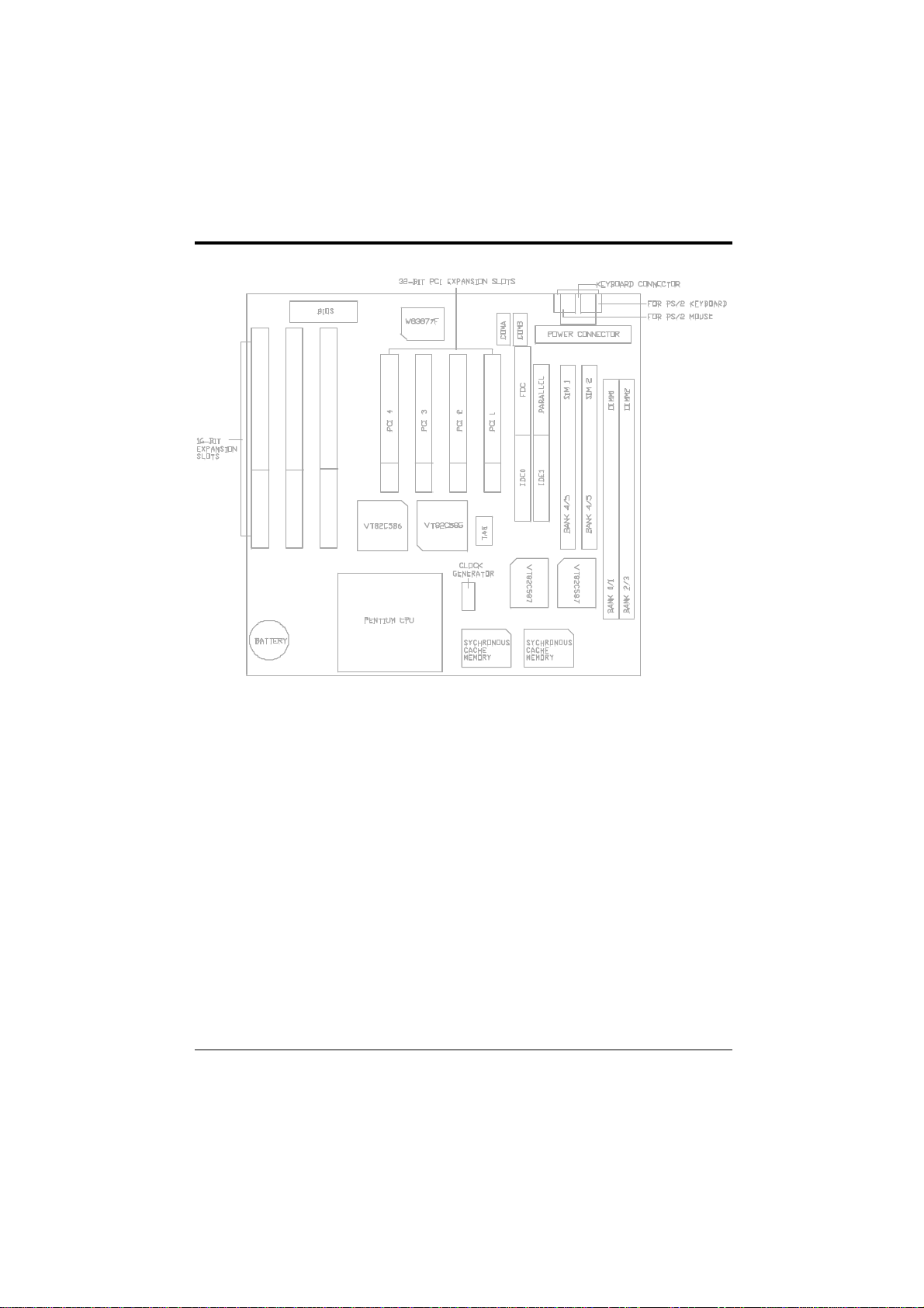
CHAPTER 1 INTRODUCTION 1
CHAPTER 2 JUMPER SETTINGS 5
2.1 JUMPERS PRESENTATION 5
2.2 CPU TYPE 5
2.2.1 INTEL PENTIUM CPU 5
2.2.2 INTEL PENTIUM w/ MMX?TECH (P55C) CPU 6
2.2.3 AMD-K6 CPU 6
2.2.4 AMD-K5 CPU 7
2.2.5 CYRIX 6x86 CPU 7
2.2.6 CYRIX 6x86L CPU 8
2.2.7 CYRIX 6x86MX CPU 8
2.2.8 IDT WinCHIP C6 CPU 9
2.3 GRAPHICAL DESCRIPTION OF JUMPER SETTINGS 10
2.4 CPU VOLTAGE 11
2.5 CPU TO BUS FREQUENCY RATIO (S7,S8,S9) 13
2.6 CPU EXTERNAL (BUS) FREQUENCY SELECTION (S10,S11,S12) 13
2.7 CPU SPEED (S7 -S12) 13
2.8 JP2 -CLEAR CMOS DATA 15
2.9 JP4 -VOLTAGE SELECTION FOR SYSTEM ROM 16
2.10 MEMORY CONFIGURATION 17
CHAPTER 3 CONNECTOR CONFIGURATION 19
3.1 J1 -RESET SWITCH, SMI SWITCH, SPEAKER, TURBO LED,
KEYLOCK AND HDD LED CONNECTOR 20
3.2 J9 -IrDA AND FAST IR CONNECTOR 20
3.3 J10, J11 -PRIMARY/SECONDARY IDE CONNECTORS 21
3.4 J12 -FLOPPY DRIVE CONTROLLER 21
3.5 J13 -PARALLEL PORT CONNECTOR 21
3.6 J14, J15 -SERIAL PORT 1 AND 2 21
3.7 J16, J17 -UNIVERSAL SERIAL BUS PORTS 0 & 1 21
3.8 J18 -EXTENSION PS/2 MOUSE CONNECTOR 22
3.9 J23 POWER SUPPLY CONNECTOR 22
CHAPTER 4 AWARD BIOS SETUP GUIDE 23
4.1 AWARD BIOS SETUP 23
4.2 STANDARD CMOS SETUP 25
4.3 BIOS FEATURES SETUP 27
4.4 CHIPSET FEATURES SETUP 29
4.5 POWER MANAGEMENT SETUP MENU 31
4.6 PCI CONFIGURATION 33
4.7 INTEGRATED PERIPHERALS SETUP MENU 35
4.8 LOAD SETUP DEFAULTS MENU 37

III
4.9 SUPERVISOR PASSWORD 37
4.10 USER PASSWORD 38
4.11 IDE HDD AUTO DETECTION 38
4.12 SCSI HARD DISK INSTALLATION 38
4.13 SAVE & EXIT SETUP MENU 38
4.14 EXIT WITHOUT SAVING MENU 39
CHAPTER 5 FLASH AND DMI UTILITY 40
5.1 AWARD FLASH UTILITY 40
5.2 DESKTOP MANAGEMENT INTERFACE (DMI) OVERVIEW 42
APPENDIX A QUICK GUIDE 46


1
CHAPTER 1 INTRODUCTION
Preface
The motherboard is a 4 layer, 2/3 baby AT size high performance mainboard. It is developed
around the pentium microprocessor with 64 bit access to data transfer and MMX technology. It
includes VIA VT82C580VPX Apollo-VPX System Chipset, Winbond W83877F Super I/O Chip.
Features
Processor
?? Intel Pentium/MMX, Cyrix 6x86/6x86L/6x86MX and AMD K5/K6 CPU.
?? The mainboard can run with following speeds:
90, 100, 120, 133, 150, 166, 200, 233, 266 and 300MHz
Chipset
?? VIA VT82C585VP (System Controller)
?? VIA VT82C586 (ISA Bus and IDE Controller)
?? VIA VT82C587VP (Data Buffer)
?? Winbond W83877F (Super I/O Controller)
Cache Size
?? Built in 0/256/512KB Synchronised Pipelined Burst Mode SRAM to achieve the high
Pentium system performance.
Main Memory
?? Support Mixed Memory Technologies: Extend Data Output (EDO), Standard Page Mode
(SPM), Fast Page Mode (FPM) and Synchronous DRAM (SDRAM) can work together.
?? Memory configurations from 4MB to 256MB are possible using combination of 512K*32 to
8M*32 SIMM module (32 bit no-parity 72-pin SIMM module) and 2M*32 to 8M*32
SDRAM DIMM module.
?? DIMM socket for SDRAM (3.3V unbuffered).
Multi I/O
?? On board Multi-I/O supports two serial, one parallel ports and floppy drive controller.
?? Serial ports are 16550 Fast UART compatible.
?? Parallel port has EPP and ECP capabilities.
?? PS/2 keyboard and PS/2 mouse connector is provided.
?? IrDA and optional Fast IR is provided.
?? Two standard USB connectors are provided.

Chapter 1
2
Fig. 1 Key Components of the Mainboard

Introduction
3
PCI IDE
?? On board supports PCI Master IDE Controller, two connectors support up to four IDE
devices such as HDD, CD ROM drive and Tape Back-up drives LS-120, etc.
?? PCI Master IDE controller supports PIO Mode 3 and 4 devices, I/O data transfer rate can
be up to 17Mb/s.
?? Ultra DMA Mode supported. Transfer rate can be up to 33MB/s.
System BIOS
?? Award BIOS (128KB Flash EPROM).
Slots
?? Four PCI slots
?? Three ISA slots
Form Factor
?? 220mm (W) x 230mm (L) 4 Layer
Environment
Working Specifications
Actual Field MTBF (hours) 104,515 hours
Preventive Maintenance Not Required
Environmental Limits
Operating Non-operating
Temperature 0 to 50 degree Celsius -10 to 65 Degree Celsius
Relative Humidity
(without condensation) 8 to 85% 5 to 95%
Altitude 10,000ft 40,000ft
Vibration 1,000Hz
Electricity 4.75 ?5.25V

Chapter 1
4

5
CHAPTER 2 JUMPER SETTINGS
2.1 JUMPERS PRESENTATION
Pins 1 and 2 are shorted with a jumper cap.
1 2 3
Pins 2 and 3 are shorted with a jumper cap.
1 2 3
The jumper is shorted when the jumper cap is placed
over the two pins of the jumper.
The jumper is open when the jumper cap is removed
from jumper.
2.2 CPU TYPE
2.2.1 INTEL PENTIUM CPU
The pentium processors have different operation voltage. In order to using the CPU
Voltage correctly, the following is the marking for identify the CPU type.
Fig. 2a CPU Description
(Bottom Side)
Description :
X = Voltage Specification (S or V) Y = Timing Specification (S or M)
S = Standard Voltage (3.4V) S = Standard EDS timings
V = VRE 3.4 -3.6V (3.5V) M = Min Valid Delay Spec.
Z = Dual Processing Support ( S or U)
S = Support DP/MP/UP
U = Not tested to support DP

Chapter 2
6
2.2.2 INTEL PENTIUM w/ MMX?TECH (P55C) CPU
The Intel Pentium w/ MMX?Tech (P55C) CPU is offered with dual voltage supply -
2.8V for core and 3.3V (I/O) interface. The following is the marking for identify the
CPU type. (The following diagram is provided as an example only. It does not
necessarily indicate a valid product marking.)
Fig. 2b CPU Description
(Top Side)
2.2.3 AMD-K6 CPU
The AMD-K6 CPU family require dual voltage power for operation. The AMD-
K6/166, 200 require a voltage of 2.9V core and 3.3V I/O. The AMD-K6/233 require a
voltage of 3.2V core and 3.3V I/O. (The following diagram is provided as an example
only. It does not necessarily indicate a valid product marking.)
Fig. 2c CPU Description
(Top Side)
Operating Voltage I/O Voltage Core Voltage
2.2V 3.3V 2.2V
2.9V 3.3V 2.9V
3.2V 3.3V 3.2V

Jumper Settings
7
2.2.4 AMD-K5 CPU
The AMD-K5 family CPU operates on different operation voltage depending on the
CPU type. The operating voltage can be known through the marking on the surface of
the CPU. (The following diagram is provided as an example only. It does not
necessarily indicate a valid product marking.)
Fig. 2d CPU Description
(Top Side)
2.2.5 CYRIX 6x86 CPU
The Cyrix 6x86 has different nominal voltage depends on different lot. Please refer to
the CPU marking.
Fig. 2e CPU Description
(Top Side)
Marketing Recommended Nominal Voltage
3.3V or 3.52V 3.52V
028 3.52V
016 3.3V
Blank 3.52V

Chapter 2
8
2.2.6 CYRIX 6x86L CPU
The Cyrix 6x86L has different I/O and core voltage. Please refer to the CPU marking.
Fig. 2f CPU Description
(Top Side)
2.2.7 CYRIX 6x86MX CPU
The Cyrix 6x86MX has different I/O and Core Voltage. Please refer to the CPU
marking.
Fig. 2g CPU Description
(Top Side)
I/O Voltage Core Voltage
Cyrix 6x86MX 3.3V 2.9V
Cyrix 6x86L 3.3V 2.8V

Jumper Settings
9
2.2.8 IDT WinCHIP C6 CPU
The IDE WinChip C6 CPU has different operation voltage. Please refer to the CPU
marking to identify the operating voltage.
Fig. 2h CPU Description

Chapter 2
10
2.3 GRAPHICAL DESCRIPTION OF JUMPER
SETTINGS
Fig. 3 Jumper Location of the mainboard

Jumper Settings
11
2.4 CPU VOLTAGE
1. 3.3V Single Voltage CPU: P54C, P54CT, 3.3V IDT WinChip C6
Fig. 4a CPU Type -3.3V
2. 3.5V Single Voltage CPU: P54C-VRE, AMD-K5, Cyrix 6x86,
3.5V IDT WinChip C6
Fig. 4b CPU Type -3.5V
3. 3.3V (I/O)/2.8V (core) Dual Voltage CPU: P55C, Cyrix 6x86L
Fig. 4c CPU Type -3.3V/2.8V

Chapter 2
12
4. 3.3V (I/O)/2.9V (core) Dual Voltage CPU: AMD-K6/166 and 200, Cyrix 6x86MX,
Cyrix MII
Fig. 4d CPU Type -3.3V/2.9V
5. 3.3V (I/O)/3.2V (core) Dual Voltage CPU: AMD-K6/233
Fig. 4e CPU Type -3.3V/3.2V
6. 3.3V (I/O)/2.2V (core) Dual Voltage CPU: AMD-K6 (2.2V) and K6-2
Fig. 4f CPU Type -3.3V/2.2V

Jumper Settings
13
2.5 CPU TO BUS FREQUENCY RATIO (S7,S8,S9)
These jumpers set the frequency ratio between the Internal frequency of the CPU and
the External frequency (called the Bus clock) within the CPU. These must be set
together with the below jumpers CPU External (Bus) Frequency Selection.
2.6 CPU EXTERNAL (BUS) FREQUENCY
SELECTION (S10,S11,S12)
These switches tell the clock generator what frequency to send to the CPU. The Bus
clock times the Bus Ratio equals the CPU’s Internal frequency.
2.7 CPU SPEED (S7 -S12)
CPU Type Freq. Ratio
Bus Ratio Setting Bus Freq. Setting
Freq.
S7 S8 S9 S10 S11 S12
Pentium 90MHz
1.5x
60MHz
open open
open
close
open
open
Pentium 100MHz
1.5x
66MHz
open open
open
open open
open
Pentium 120MHz
2.0x
60MHz
close
open
open
close
open
open
Pentium 133MHz
2.0x
66MHz
close
open
open
open open
open
Pentium 150MHz
2.5x
60MHz
close
close
open
close
open
open
Pentium 166MHz
2.5x
66MHz
close
close
open
open open
open
Pentium 200MHz
3.0x
66MHz
open close
open
open open
open
Pentium w/MMX 166MHz
2.5x
66MHz
close
close
open
open open
open
Pentium w/MMX 200MHz
3.0x
66MHz
open close
open
open open
open
Pentium w/MMX 233MHz
3.5x
66MHz
open open
open
open open
open
AMD-K5-PR166 166MHz
2.5x
66MHz
close
close
open
open open
open
AMD-K5-PR133 133MHz
2.0x
66MHz
close
open
open
open open
open
AMD-K5-PR120 120MHz
2.0x
60MHz
close
open
open
close
open
open
AMD-K6/300 300MHz
4.5x
66MHz
close
close
close
open open
open
AMD-K6/266 266MHz
4.0x
66MHz
close
open
close
open open
open
AMD-K6-2/266 266MHz
4.0x
66MHz
close
open
close
open open
open
AMD-K6/233 233MHz
3.5x
66MHz
open open
open
open open
open
AMD-K6/200 200MHz
3.0x
66MHz
open close
open
open open
open
To be continued.....
Table 1a

Chapter 2
14
CPU Type Freq. Ratio
Bus Ratio Setting Bus Freq. Setting
Freq.
S7 S8 S9 S10 S11 S12
AMD-K6/166 166MHz
2.5x
66MHz
close
close
open
open open
open
Cyrix MII-300 233MHz
3.5x
66MHz
open open
open
open open
open
Cyrix MII-300 225MHz
3.0x
75MHz
open close
open
open close
open
Cyrix 6x86MX-PR233
200MHz
3.0x
66MHz
open close
open
open open
open
Cyrix 6x86MX-PR233
188MHz
2.5x
75MHz
close
close
open
open close
open
Cyrix 6x86MX-PR200
166MHz
2.5x
66MHz
close
close
open
open open
open
Cyrix 6x86MX-PR200
150MHz
2.0x
75MHz
close
open
open
open close
open
Cyrix 6x86MX-PR166
150MHz
2.5x
60MHz
close
close
open
close
open
open
Cyrix 6x86L-PR200 150MHz
2.0x
75MHz
close
open
open
open close
open
Cyrix 6x86L-PR166 133MHz
2.0x
66MHz
close
open
open
open open
open
Cyrix 6x86L-PR150 120MHz
2.0x
60MHz
close
open
open
close
open
open
IDT WinChip C6-180
180MHz
3x 60MHz
open close
open
close
open
open
IDT WinChip C6-200
200MHz
3x 66MHz
open close
open
open open
open
Table 1b
Reserve for future support
Fig. 5 Example: CPU speed jumper setting for
200MHz Intel Pentium w/ MMX
This manual suits for next models
1
Table of contents
Other DTK Motherboard manuals
Popular Motherboard manuals by other brands

Linear Technology
Linear Technology DC1884A Series Demo Manual

Gigabyte
Gigabyte GA-7A8DRH user manual

Avalue Technology
Avalue Technology EPX-APLP user manual

Epson
Epson S1V3034x Series Start guide

Texas Instruments
Texas Instruments ADS7861EVM user guide

Allegro MicroSystems
Allegro MicroSystems APEK4964 user manual

Leadtek
Leadtek WinFast K7N420DA user manual

National Semiconductor
National Semiconductor ADS42B4 Series user guide

Biostar
Biostar M7VIB datasheet

Texas Instruments
Texas Instruments SWIFT TPS54350EVM-235 user guide

ECS Electronics
ECS Electronics SI54P AIO user manual

Gigabyte
Gigabyte GA-H61MA-D3V user manual