DTK PAM-0052V User manual

PAM-0052V
High Performance
Pentium PCI Mainboard
Edition 1.30
1999 DTK Computer, Inc.
P/N: 155100-8755

I
WARNING
For the system to operate normally, please make sure JP6 of the mainboard is set as below. Refer
to Fig. 3 in this manual for the location JP6.
If JP6 is shorted to 2-3, no CMOS data can be retained.
CAUTION
The motherboard is an electrostatic sensitive device. Don’t open or handle except at a static-
free workstation.
Windows, MS-DOS, and MS Word are trademarks of Microsoft Corporation.
Novell, Netware are trademarks of Novell, Inc.
PC, AT, PC-DOS, OS/2 and Presentation Manager are trademarks of IBM Corporation.
Pentium is registered trademark of Intel Corp.
UNIX is the trademark of AT&T.
All other brand and product names are trademarks or registered trademarks of their respective
companies.
The information presented in this publication has been carefully checked for reliability; however,
no responsibility is assumed for inaccuracies, whereas, specification is subjected to change
without notice.

II
CONTENTS
CHAPTER 1 INTRODUCTION 1
CHAPTER 2 JUMPER SETTINGS 5
2.1 JUMPERS PRESENTATION 5
2.2 CPU TYPE 5
2.2.1 INTEL PENTIUM w/ MMXTECH (P55C) CPU 5
2.2.2 AMD-K6 CPU 6
2.2.3 CYRIX 6x86L CPU 6
2.2.4 CYRIX 6x86MX CPU 7
2.3 GRAPHICAL DESCRIPTION OF JUMPER SETTINGS 8
2.4 CPU VOLTAGE 9
2.5 CPU TO BUS FREQUENCY RATIO (SW1-4,5,6) 10
2.6 CPU EXTERNAL (BUS) FREQUENCY SELECTION (SW1-7,8,9,10) 10
2.7 SDRAM FREQUENCY SELECTION (SW-10) 10
2.8 CPU SPEED 11
2.9 JP6 – CLEAR CMOS DATA 12
2.10 MEMORY CONFIGURATION 13
CHAPTER 3 CONNECTOR CONFIGURATION 15
3.1 J1 – MULTIPLE FUNCTION JUMPER 16
3.2 J2 – CPU FAN CONNECTION 16
3.3 J3 - IrDA/FAST IR CONNECTOR 17
3.4 J4 – UNIVERSAL SERIAL BUS PORTS 0 & 1 17
3.5 J5, J6 - PRIMARY/SECONDARY IDE CONNECTOR 17
3.6 J7 - ATX POWER CONNECTOR 18
3.7 J8 – PARALLEL PORT CONNECTOR 18
3.8 J9 - FLOPPY DRIVE CONNECTOR 18
3.9 J10 – EXTENSION PS/2 MOUSE CONNECTOR 18
3.10 J11 – KEYBOARD CONNECTOR 19
3.11 J12, J13 - SERIAL PORT COM1/COM2 19
3.12 J14 – INTERNAL MODEM RING-IN CONNECTOR 19
3.13 J15 - AT POWER CONNECTOR 20
3.14 CN2 – PS/2 STYLE KEYBOARD CONNECTOR (OPTIONAL) 20
CHAPTER 4 AWARD BIOS SETUP GUIDE 21
4.1 AWARD BIOS SETUP 21
4.2 STANDARD CMOS SETUP 23
4.3 BIOS FEATURES SETUP 24
4.4 CHIPSET FEATURES SETUP 26
4.5 POWER MANAGEMENT SETUP MENU 28
4.6 PCI CONFIGURATION 30
4.7 INTEGRATED PERIPHERALS SETUP MENU 32
4.8 LOAD SETUP DEFAULTS MENU 34
4.9 SUPERVISOR PASSWORD 34

III
4.10 USER PASSWORD 34
4.11 IDE HDD AUTO DETECTION 35
4.12 SAVE & EXIT SETUP MENU 35
4.13 EXIT WITHOUT SAVING MENU 35
CHAPTER 5 FLASH AND DMI UTILITY 37
5.1 AWARD FLASH UTILITY 37
5.2 DESKTOP MANAGEMENT INTERFACE (DMI) OVERVIEW 39
APPENDIX A QUICK GUIDE 43

1
CHAPTER 1 INTRODUCTION
Preface
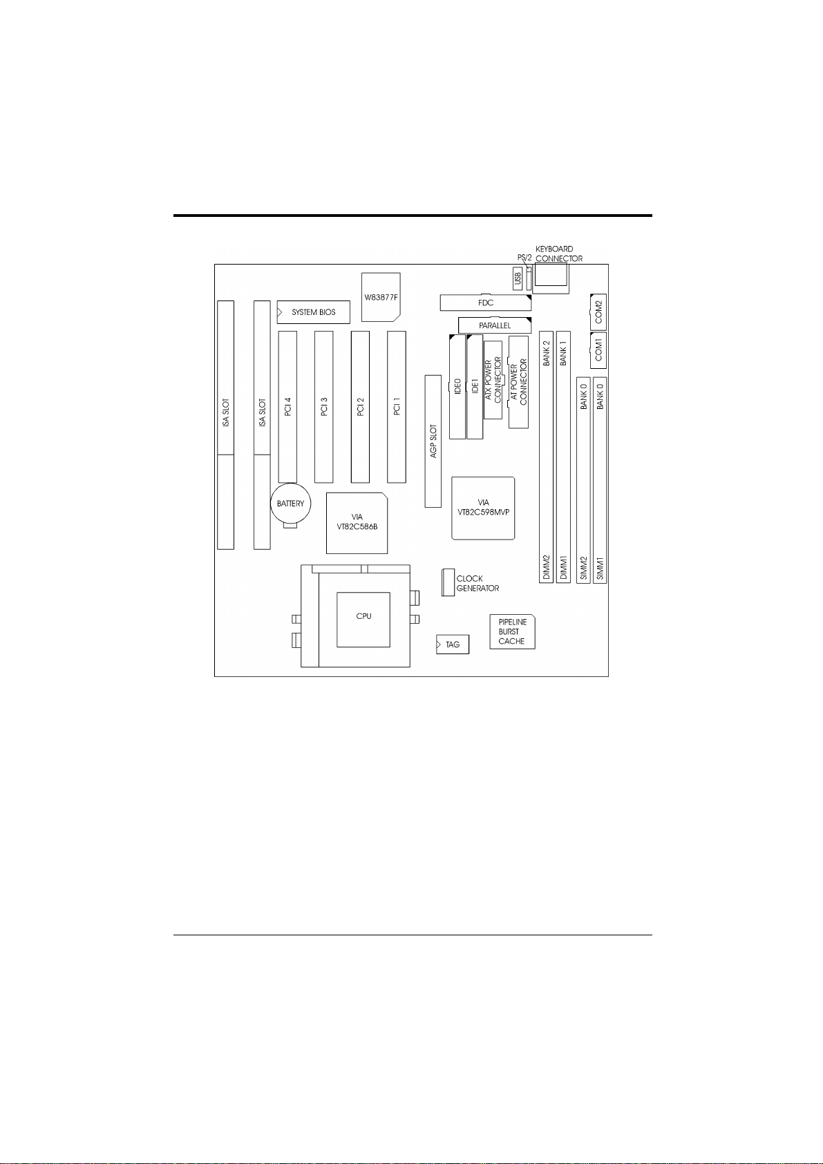
The motherboard is a 4-layer, 2/3 baby AT size high performance mainboard. It includes VIA
VT82C598MVP (MVP3) system chipset, Winbond W83877F super I/O chip.
Features
Processor
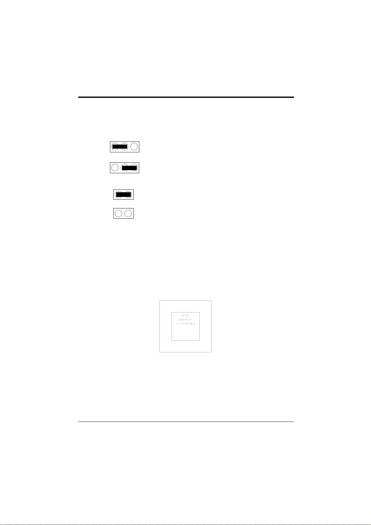
•Intel Pentium/MMX, Cyrix 6x86L/6x86MX/M II and AMD K6/K6-2 CPU.
•The mainboard can run with following speeds:
90, 100, 110, 120, 133, 150, 166, 200, 233, 250, 266, 300, 333, 350, 366, 380, 400 and
450MHz
Chipset
•VIA VT82C598MVP (VIA MVP3 System Controller)
•VIA VT82C586B (PCI ISA IDE Xcelerator)
•Winbond W83877F Super I/O Controller
Cache Size
•Built in 0/512KB Synchronised Pipelined Burst Mode SRAM to achieve the high Pentium
system performance.
Main Memory
•Support Mixed Memory Technologies: Extend Data Output (EDO), Standard Page Mode
(SPM) and Fast Page Mode (FPM) and Synchronous DRAM (SDRAM) can work together.
•Memory configurations from 8MB to 384MB are possible using combination of 1M*32 to
8M*32 module (32 bit no-parity 72-pin SIMM module) and 2M*64 to 16M*64 SDRAM
DIMM module.
Multi I/O
•On board Multi-I/O supports two serial, one parallel ports and floppy drive controller.
•Serial ports are 16550 Fast UART compatible.
•Parallel port has EPP and ECP capabilities.
•PS/2 mouse and keyboard supported.
•IrDA supported.
•Dual standard USB (Universal Serial Bus) ports supported.
PCI IDE
•On board supports PCI Master IDE Controller, two connectors support up to four IDE
devices such as HDD, CD ROM drive and Tape Back-up drives, etc.
•PCI Master IDE controller supports PIO Mode 3 and 4 devices, I/O data transfer rate can be
up to 17Mb/s. DMA mode transfer rate can be up to 22Mb/s.
•Ultra DMA Mode supported. Transfer rate can be up to 33Mb/s.

Chapter 1
2
Fig. 1 Key Components of the Mainboard
System BIOS
•Award BIOS (128KB Flash EPROM).
Slots
•Four PCI slots
•Two ISA slots
Form Factor
•2/3 Baby AT size (220mm x 230mm)

Introduction
3
Environment
Working Specifications
Actual Field MTBF (hours) 104,515 hours
Preventive Maintenance Not Required
Environmental Limits Operating Non-operating
Temperature 0 to 50 degree Celsius -10 to 65 Degree Celsius
Relative Humidity
(without condensation) 8 to 85% 5 to 95%
Altitude 10,000ft 40,000ft
Vibration 1,000Hz
Electricity 4.75 ∼5.25V
Power Specification
Configuration: 133MHz Intel P54C CPU, 16MB 60ns EDO SIMM, 512KB Cache, 3.5 inch
floppy drive, 840MB Hard Disk, running at DOS prompt.
DC Voltage Tolerance Consumption (mA)
+5V +/- 5% 860
+5V Standby +/- 5% 0.5
+5V +/- 5% 0
+12V +/- 5% 200
-12V +/- 5% 30

Chapter 1
4

5
CHAPTER 2 JUMPER SETTINGS
2.1 JUMPERS PRESENTATION
Pins 1 and 2 are shorted with a jumper cap.
1 2 3
Pins 2 and 3 are shorted with a jumper cap.
1 2 3
The jumper is shorted when the jumper cap is placed
over the two pins of the jumper.
The jumper is open when the jumper cap is removed
from jumper.
2.2 CPU TYPE
2.2.1 INTEL PENTIUM w/ MMX TECH (P55C) CPU
The Intel Pentium w/ MMXTech (P55C) CPU is offered with dual voltage supply
- 2.8V for core and 3.3V (I/O) interface. The following is the marking for identify
the CPU type. (The following diagram is provided as an example only. It does not
necessarily indicate a valid product marking.)
Fig. 2a CPU Description
(Top Side)

Chapter 2
6
2.2.2 AMD-K6 CPU
The AMD-K6 CPU family require dual voltage power for operation. The AMD-
K6/166, 200 require a voltage of 2.9V core and 3.3V I/O. The AMD-K6/233
require a voltage of 3.2V core and 3.3V I/O. (The following diagram is provided as
an example only. It does not necessarily indicate a valid product marking.)
Fig. 2b CPU Description
(Top Side)
Operating Voltage I/O Voltage Core Voltage
2.2V 3.3V 2.2V
2.4V 3.3V 2.4V
2.9V 3.3V 2.9V
3.2V 3.3V 3.2V
2.2.3 CYRIX 6x86L CPU
The Cyrix 6x86L has different I/O and core voltage. Please refer to the CPU
marking.
Fig. 2c CPU Description
(Top Side)

Jumper Settings
7
2.2.4 CYRIX 6x86MX CPU
The Cyrix 6x86MX has different I/O and Core Voltage. Please refer to the CPU
marking.
Fig. 2d CPU Description
(Top Side)
I/O Voltage Core Voltage
Cyrix 6x86MX 3.3V 2.9V
Cyrix 6x86L 3.3V 2.8V

Chapter 2
8
2.3 GRAPHICAL DESCRIPTION OF JUMPER
SETTINGS
Fig. 3 Jumper Location of the mainboard

Jumper Settings
9
2.4 CPU VOLTAGE
The CPU Core Voltage can be selected by SW1-1,2,3.
CPU Voltage SW1
3.3V (I/O)/2.2V (core) Dual Voltage CPU
For 2.2V AMD-K6 and AMD-K6-2
3.3V (I/O)/2.4V (core) Dual Voltage CPU
For 2.4V AMD-K6-III
3.3V (I/O)/2.8V (core) Dual Voltage CPU
For P55C and Cyrix 6x86L
3.3V (I/O)/2.9V (core) Dual Voltage CPU
For 2.9V AMD-K6, Cyrix 6x86MX and
Cyrix M II
3.3V (I/O)/3.2V (core) Dual Voltage CPU
For 3.2V AMD-K6/233
Table 1
1 2 3
ON
1 2 3
ON
1 2 3
ON
1 2 3
ON
1 2 3
ON

Chapter 2
10
2.5 CPU TO BUS FREQUENCY RATIO (SW1-4,5,6)
These switches set the frequency ratio between the Internal frequency of the CPU
and the External frequency (called the Bus clock) within the CPU. These must be
set together with the above jumpers CPU External (Bus) Frequency Selection.
2.6 CPU EXTERNAL (BUS) FREQUENCY SELECTION
(SW1-7,8,9,10)
These switches tell the clock generator what frequency to send to the CPU. The Bus
clock times the Bus Ratio equals the CPU’s Internal frequency.
2.7 SDRAM FREQUENCY SELECTION (SW-10)
This switch set the SDRAM frequency same as CPU External frequency or AGP
frequency.
SW1-10 : ON SDRAM frequency = AGP frequency
SW1-10 : OFF SDRAM frequency = CPU External frequency
4 5 6 7 8 9 10
ON

Jumper Settings
11
2.8 CPU SPEED
CPU Type Freq. Ratio Freq. Ratio Setting Bus Freq. Setting
CPU Bus
Freq. SW1-4 SW1-5 SW1-6 SW1-7 SW1-8 SW1-9
Intel Pentium w/MMX 166MHz 2.5x 66MHz ON ON OFF OFF ON ON
Intel Pentium w/MMX 200MHz 3.0x 66MHz OFF ON OFF OFF ON ON
Intel Pentium w/MMX 233MHz 3.5x 66MHz OFF OFF OFF OFF ON ON
AMD-K6/166 166MHz 2.5x 66MHz ON ON OFF OFF ON ON
AMD-K6/200 200MHz 3.0x 66MHz OFF ON OFF OFF ON ON
AMD-K6/233 233MHz 3.5x 66MHz OFF OFF OFF OFF ON ON
AMD-K6/266 266MHz 4.0x 66MHz ON OFF ON OFF ON ON
AMD-K6/300 300MHz 4.5x 66MHz ON ON ON OFF ON ON
AMD-K6-2/250 250MHz 2.5x 100MHz ON ON OFF OFF OFF OFF
AMD-K6-2/266 266MHz 4.0x 66MHz ON OFF ON OFF ON ON
AMD-K6-2/300 300MHz 3.0x 100MHz OFF ON OFF OFF OFF OFF
AMD-K6-2/333 333MHz 3.5x 95MHz OFF OFF OFF ON OFF OFF
AMD-K6-2/350 350MHz 3.5x 100MHz OFF OFF OFF OFF OFF OFF
AMD-K6-2/366 366MHz 5.5x 66MHz OFF OFF ON OFF ON ON
AMD-K6-2/380 380MHz 4.0x 95MHz ON OFF ON ON OFF OFF
AMD-K6-2/400 400MHz 4.0x 100MHz ON OFF ON OFF OFF OFF
AMD-K6-2/450 450MHz 4.5x 100MHz ON ON ON OFF OFF OFF
AMD-K6-III/400 400MHz 4.0x 100MHz ON OFF ON OFF OFF OFF
AMD-K6-III/450 450MHz 4.5x 100MHz ON ON ON OFF OFF OFF
Cyrix 6x86L-PR150 120MHz 2.0x 60MHz ON OFF OFF ON ON ON
Cyrix 6x86L-PR166 133MHz 2.0x 66MHz ON OFF OFF OFF ON ON
Cyrix 6x86L-PR200 150MHz 2.0x 75MHz ON OFF OFF ON ON OFF
Cyrix 6x86MX-PR166 150MHz 2.5x 60MHz ON ON OFF ON ON ON
Cyrix 6x86MX-PR200 150MHz 2.0x 75MHz ON OFF OFF ON ON OFF
Cyrix 6x86MX-PR200 166MHz 2.5x 66MHz ON ON OFF OFF ON ON
Cyrix 6x86MX-PR233 188MHz 2.5x 75MHz ON ON OFF ON ON OFF
Cyrix 6x86MX-PR233 200MHz 3.0x 66MHz OFF ON OFF OFF ON ON
Cyrix M II-300 225MHz 3.0x 75MHz OFF ON OFF ON ON OFF
Cyrix M II-300 233MHz 3.5x 66MHz OFF OFF OFF OFF ON ON
Cyrix M II-333 250MHz 2.5x 100MHz ON ON OFF OFF OFF OFF
Cyrix M II-333 250MHz 3.0x 83MHz OFF ON OFF OFF ON OFF
Cyrix M II-350 300MHz 3.0x 100MHz OFF ON OFF OFF OFF OFF
IBM 6x86MX-PR266 208MHz 2.5x 83MHz ON ON OFF OFF ON OFF
Table 2
Reserve for future support

Chapter 2
12
2.9 JP6 – CLEAR CMOS DATA
1. Normal Mode
Fig. 4a
2. Reset Content of RTC
Fig. 4b

Jumper Settings
13
2.10 MEMORY CONFIGURATION
The mainboard lets user upgrade system memory via SIMM or DIMM sockets on the
mainboard. On board memory is located in three banks: Bank 0 – Bank 2. Two
SIMM sockets (SIMM1, SIMM2) are provided for SPM, FPM and EDO RAM
SIMM and two DIMM sockets (DIMM1, DIMM2) are available for the 3.3V
unbuffered SDRAM and EDO DIMM.
Note: The type of SIMM1/SIMM2 must be same.
Only 3.3V unbuffered DIMM can be used.
Both single sided and double sided SIMM or DIMM can be supported.
Table 4 provides the typical memory configurations supported by the mainboard.
Bank 0
(SIMM1/2) Bank 1
(DIMM1) Bank 2
(DIMM2)
Installed None None
Installed Installed None
None Installed None
Installed None Installed
None None Installed
Installed Installed Installed
None Installed Installed
Table 3
The memory size of SIMM can be 8MB, 16MB, 32MB or 64MB. The memory of
DIMM can be 8MB, 16MB, 32MB, 64MB or 128MB.
Important: When 100MHz DRAM speed is selected. SDRAM DIMMs with
PC100 specification and Serial Presence Defect (SPD) data structure
are required.
We highly don’t recommend the mix combination of SIMMs and
DIMMs, especially when 100MHz DRAM speed is selected.

Chapter 2
14

15
CHAPTER 3 CONNECTOR
CONFIGURATION
Once the mainboard has been fastened into system case, the next step is to connect the internal
cables and external cables. The mainboard connectors have varying numbers of pins and are the
points of contact between the mainboard and other parts of the computer.
Fig. 5 Connector Location

Chapter 3
16
3.1 J1 – MULTIPLE FUNCTION JUMPER
J1 is a front panel multi-function jumper include speaker, reset, keylock, harddisk,
LED, ATX power switch, ACPI (suspend) LED and power button (suspend switch).
The pin definition is as following figure.
Fig. 6 Multiple Function Jumper
3.2 J2 – CPU FAN CONNECTION
J2 is a three pin connector, which is used to connect with the CPU FAN power
cable.
Fig. 7 CPU Fan Connector
1 2 3
Table of contents
Other DTK Motherboard manuals