DTK PRM-0081I User manual

PRM-0081I
High Performance
Dual Pentium II
AGP/PCI Mainboard
User’s Guide
Edition 1.00
©1998 DTK Computer, Inc.
P/N: 155100-8664


I
WARNING
For the system to operate normally, please make sure JP2 of the mainboard is set as below. Refer
to Fig. 2 in this manual for the location JP2.
If JP2 is shorted to 2-3, no CMOS data can be retained.
CAUTION
The motherboard is an electrostatic sensitive device. Don’t open or handle except at a static-
free workstation.
POWER OFF
It needs to hold the power switch 4 seconds to turn off the power.
Windows, MS-DOS, and MS Word are trademarks of Microsoft Corporation.
Novell, Netware are trademarks of Novell, Inc.
Lotus, 1-2-3, and Symphony are trademarks of Lotus Development Corporation.
PC, AT, PC-DOS, OS/2 and Presentation Manager are trademarks of IBM Corporation.
UNIX is the trademark of AT&T.
Intel i82440BX and Pentium II are registered trademark of Intel Corporation.
All other brand and product names are trademarks or registered trademarks of their respective
companies.
The information presented in this publication has been carefully checked for reliability; however,
no responsibility is assumed for inaccuracies, whereas, specification is subjected to change
without notice.
1 2 3
JP2

II
CONTENTS
CHAPTER 1 INTRODUCTION 1
CHAPTER 2 JUMPER SETTINGS 3
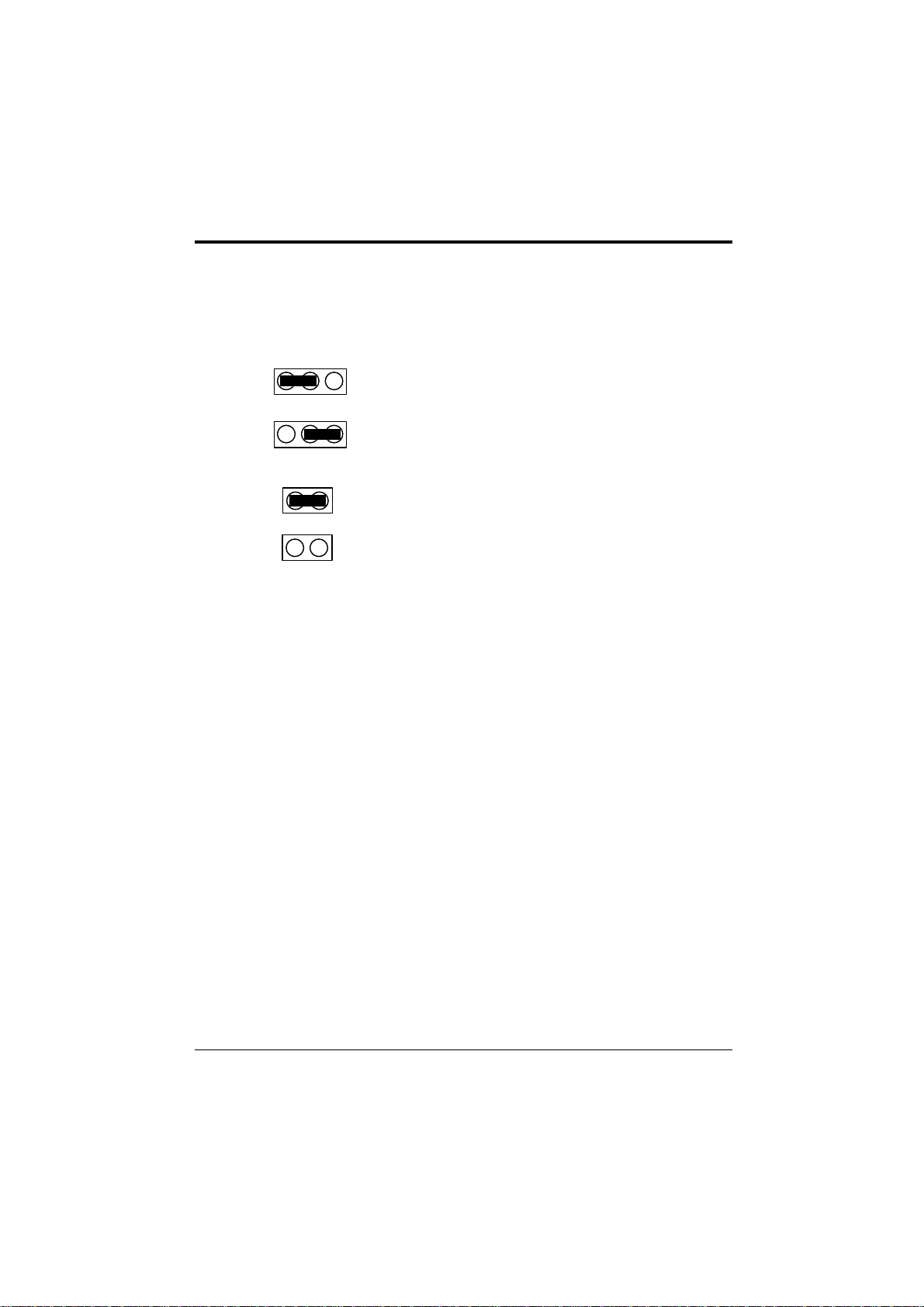
2.1 JUMPERS PRESENTATION 3
2.2 GRAPHICAL DESCRIPTION OF JUMPER SETTINGS 4
2.3 CPU SPEED 5
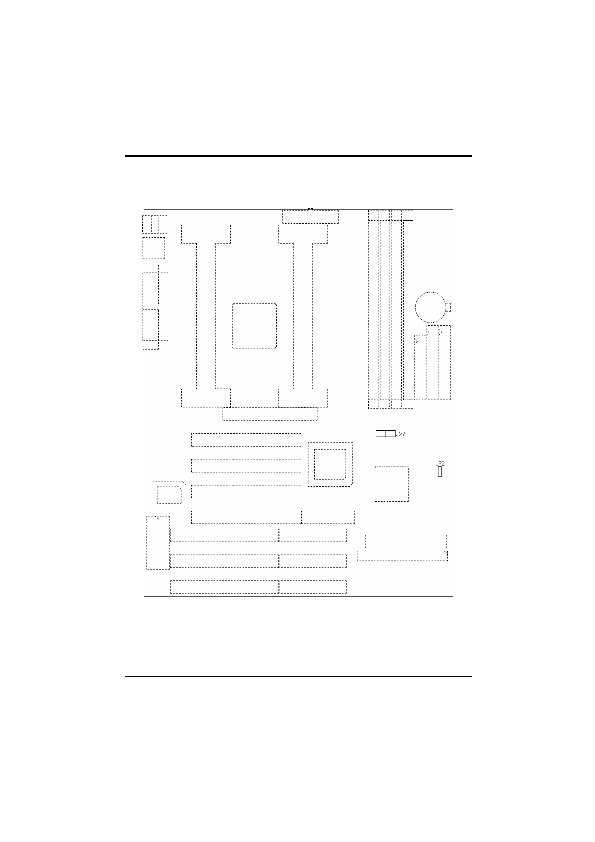
2.4 JP2 - CLEAR CMOS DATA 5
2.5 MEMORY CONFIGUARTION 6
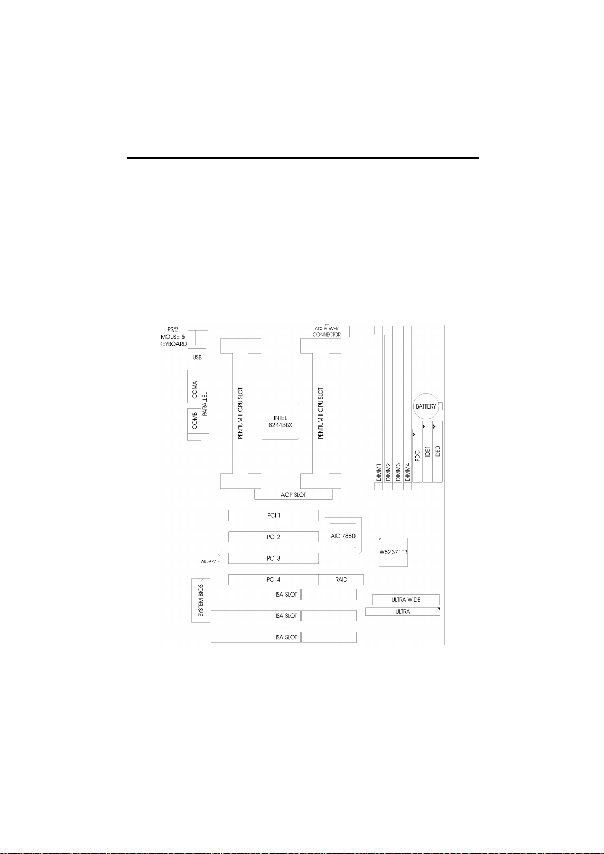
CHAPTER 3 CONNECTOR CONFIGURATION 7
3.1 J1, J2 - SLOT 1 FOR PENTIUM II CPU 8
3.2 J3, J4 - PRIMARY/SECONDARY IDE CONNECTORS 8
3.3 J7 - ATX POWER SUPPLY CONNECTOR 8
3.4 J8 - RESET 9
3.5 J9 - POWER LED 9
3.6 J10 - HDD LED 9
3.7 J11 - POWER ON/OFF SWITCH 9
3.8 J12 - SPEAKER 10
3.9 J13, J14, J15 - CPU FAN CONNECTOR 10
3.10 J16 - IrDA CONNECTOR 10
3.11 J22 - FLOPPY DRIVE CONTROLLER 10
3.12 J24 - SCSI CONNECTOR 11
3.13 J25 - ULTRA WIDE SCSI CONNECTOR 11
3.14 JP10 – SCSI LED 11
3.15 JP26 - WAKE ON LAN CONNECTOR 11
3.16 PS/2 KEYBOARD CONNECTOR 12
3.17 PS/2 MOUSE CONNECTOR 12
3.18 UNIVERSAL SERIAL BUS PORT 0 & 1 12
3.19 SERIAL PORT COM1 & COM2 12
3.20 PARALLEL PORT CONNECTOR 12
3.21 RETENTION MECHANISM KITS INSTALLATION GUIDE 13
CHAPTER 4 AWARD BIOS SETUP GUIDE 17
4.1 AWARD BIOS SETUP 17
4.2 STANDARD CMOS SETUP 19
4.3 BIOS FEATURES SETUP 20
4.4 CHIPSET FEATURES SETUP 21
4.6 PCI CONFIGURATION 25
4.7 INTEGRATED PERIPHERALS SETUP MENU 27
4.8 LOAD SETUP DEFAULTS MENU 29
4.9 SUPERVISOR PASSWORD 29
4.10 USER PASSWORD 29
4.11 IDE HDD AUTO DETECTION 30

III
4.12 SAVE & EXIT SETUP MENU 30
4.13 EXIT WITHOUT SAVING MENU 30
CHAPTER 5 FLASH AND DMI UTILITY 31
5.1 AWARD FLASH UTILITY 31
5.2 DESKTOP MANAGEMENT INTERFACE (DMI) OVERVIEW33
APPENDIX A QUICK GUIDE 37


1
CHAPTER 1 INTRODUCTION
Preface
The motherboard is a 4 layer, ATX form factor high performance Dual Pentium II AGP/PCI
mainboard. It includes Intel i82440BX system chipset, Winbond W83977TF Super I/O
controller and Adaptec AIC-7880 SCSI controller.
Features
Processor
•Intel Dual Pentium II series.
•The mainboard can run with following speeds:
350, 400, and 450MHz
Chipset
•Intel i82443BX (PCI A.G.P. Controller)
•Intel 82371EB (PCI ISA IDE Xcelerator)
•Winbond W83977TF (Super I/O Controller)
•Adaptec AIC-7880 (SCSI Controller)
Main Memory
•Memory configurations up to 512MB SDRAM/EDO.
•DIMM socket for SDRAM (3.3V unbuffered).
•Support both Synchronous DRAM and Extended Data Output (EDO) Mode DRAM
Modules.
•ECC Function ensures data correction and integrity.
Multi I/O
•On board Multi-I/O supports two serial, one parallel ports and floppy drive controller.
•Serial ports are 16550 Fast UART compatible.
•Parallel port has EPP and ECP capabilities.
•PS/2 keyboard and PS/2 mouse connector is provided.
•IrDA supported.
•USB supported.
Accelerated Graphics Port (AGP) Interface
•A.G.P. specification compliant
•A.G.P. 66/133MHz devices supported
PCI IDE
•On board supports PCI Master IDE Controller, two connectors support up to four IDE
devices such as HDD, CD ROM drive and Tape Back-up drives, etc.
•PCI Master IDE controller supports PIO Mode 3 and 4 devices, I/O data transfer rate can be
up to 16.6MB/s.
•Ultra DMA Mode supported. Transfer rate can be up to 33MB/s.

Chapter 1
2
PCI SCSI
•Support Double Speed SCSI operation up to 40Mbytes/sec.
•PCI Bus Master for data transfer.
•8 bit, 16 bit SCSI Bus support.
System BIOS
•Award BIOS (128KB Flash EPROM).
Slots
•One AGP slot
•Four PCI slots (1 shared)
•Three ISA slots(1 shared)
Form Factor
•Full ATX Size (305mm x 244mm) 4 Layer
Fig. 1 Key Components of the Mainboard

3
CHAPTER 2 JUMPER SETTINGS
2.1 JUMPERS PRESENTATION
Pins 2 and 3 are shorted with a jumper cap.
3 2 1
Pins 1 and 2 are shorted with a jumper cap.
3 2 1
The jumper is shorted when the jumper cap is placed
over the two pins of the jumper.
The jumper is open when the jumper cap is removed
from jumper.
Jumpers Convention
Different color of jumper caps (mini-jumpers) are used on the board to represent
different usage of the jumpers:
Red: CPU Clock setting
Black: Other

Chapter 2
4
2.2 GRAPHICAL DESCRIPTION OF JUMPER
SETTINGS
Fig. 2 Jumper Location of the mainboard

Jumper Settings
5
2.3 CPU SPEED
The table below summaries the CPU frequence and settings of each jumper of the
motherboard.
CPU Type Freq. Ratio Bus Freq. Rating Setting
Pentium II 350MHz 3.5x J27: 1 close
2 open
3 open
Pentium II 400MHz 4.0x J27: 1 open
2 close
3 close
Pentium II 450MHz 4.5x
100MHz
J27: 1 open
2 close
3 open
Table 1: Jumper Setting
2.4 JP2 - CLEAR CMOS DATA
JP2 is used to clear the content of the CMOS Data in the RTC (build in PIIX4 chip).
Table 2: Clear CMOS Data

Chapter 2
6
2.5 MEMORY CONFIGUARTION
The mainboard lets user upgrade system memory via DIMM sockets on the
mainboard. On board memory is located in eight banks: Bank 0 - 7. Four DIMM
sockets are provided for EDO DRAM or Synchronous DRAM. Table 3 provides the
typical memory configurations supported by the mainboard.
Bank 0/1 (DIMM1) Bank 2/3 (DIMM2) Bank 4/5 (DIMM3) Bank 6/7 (DIMM4)
Installed None None None
None Installed None None
None None Installed None
None None None Installed
Installed Installed None None
Installed None Installed None
Installed None None Installed
None Installed Installed None
None Installed None Installed
None None Installed Installed
Installed Installed Installed None
Installed Installed None Installed
Installed None Installed Installed
None Installed Installed Installed
Installed Installed Installed Installed
Table 3
The maximum memory size is up to 512MB (SDRAM/EDO). The size of each
DIMM can be 8MB, 16MB, 32MB, 64MB or 128MB.

7
CHAPTER 3 CONNECTOR
CONFIGURATION
Once the mainboard has been fastened into system case, the next step is to connect the internal
cables. The internal cables are wire leads with plastic female connectors that attach to the
connectors. The mainboard connectors have varying numbers of pins and are the points of
contact between the mainboard and other parts of the computer.
Fig 3 Connector Location

Chapter 3
8
3.1 J1, J2 - SLOT 1 FOR PENTIUM II CPU
J1 and J2 are the slots for Pentium II CPU.
Fig. 4 Slot 1 for Pentium CPU
3.2 J3, J4 - PRIMARY/SECONDARY IDE
CONNECTORS
These connectors support the provided IDE hard disk ribbon cable. After
connecting the single end to the board, connect the two plugs on the other end to
your hard disk or other device.
3.3 J7 - ATX POWER SUPPLY CONNECTOR
J7 is a 2x10 pin male connector. Plug the power connector of the ATX power
supply onto the connector.
Fig. 5 ATX Power Supply Connector

Connector Configuration
9
3.4 J8 - RESET
Attach the Reset switch cable to this connector. The Reset switch restarts the
system.
3.5 J9 - POWER LED
Fig. 6 Power LED
3.6 J10 - HDD LED
J10 is usually connected to a HDD LED on front of the system case. If the HDD is
in operation, the indicator lights during operation.
Fig. 7 HDD LED
3.7 J11 - POWER ON/OFF SWITCH
It is used to switch on or off the ATX power supply. The power is turned on by
short the power switch once. It needs to hold the power switch about 4 seconds to
turn it off when it has not start to display.

Chapter 3
10
3.8 J12 - SPEAKER
J12 is a four pins connector, which is used to connect the system speaker.
Fig. 8 Speaker
3.9 J13, J14, J15 - CPU FAN CONNECTOR
J13 & J14 & J15 are three pin connectors, which are used to connect with the CPU
Fan Power cable.
3.10 J16 - IrDA CONNECTOR
J16 is an IrDA connector that uses UART2 as interface of IrDA Infrared and HP
SIR.
Fig. 9 IrDA Connector
3.11 J22 - FLOPPY DRIVE CONTROLLER
This connector supports the floppy drive ribbon cable. After connecting the single
end to the board, connect the two plugs on the other end to the floppy drive.

Connector Configuration
11
3.12 J24 - SCSI CONNECTOR
J24 is a 50 pin connector for a SCSI device.
3.13 J25 - ULTRA WIDE SCSI CONNECTOR
J25 is a high density 68 pin connector for a wide SCSI device.
3.14 JP10 – SCSI LED
JP10 is usually connected to a SCSI LED on front of the system case. If the SCSI is
in operation, the indicator lights during operation.
Fig. 10 SCSI LED
3.15 JP26 - WAKE ON LAN CONNECTOR
JP26 is a 3-pin connector as interface of LAN card for wake up on LAN purpose.
Fig. 11 Wake On LAN Connector

Chapter 3
12
Fig. 12 I/O Connector
3.16 PS/2 KEYBOARD CONNECTOR
This connector is a six-pin female mini DIN connector using a PS/2 plug. If a
standard AT size keyboard plugs, you may use the DIN to mini DIN adaptor.
3.17 PS/2 MOUSE CONNECTOR
This connector is a six-pin female mini DIN connector using a PS/2 plug. Plug the
jack on the PS/2 keyboard cable into this connector.
3.18 UNIVERSAL SERIAL BUS PORT 0 & 1
These connectors are two four pin female sockets which are available for connecting
USB device.
3.19 SERIAL PORT COM1 & COM2
This is a D-Type 9 pin male connector for pointing devices or other serial devices.
3.20 PARALLEL PORT CONNECTOR
This is a D-Type 25 pin female connector.

Connector Configuration
13
3.21 RETENTION MECHANISM KITS INSTALLATION
GUIDE
Retention Mechanism Kits includes following components:
1. Retention mechanism Assembly
Fig. 13
2. Retention Mechanism Attach Mount
Fig. 14

Chapter 3
14
3. Heatsink Top Support
Fig. 15
4. Heatsink Support Base
Fig. 16
Before the installation of RM Kits find the six holes on the motherboard for RM installation.
The hole position and usage is as following:
Fig. 17
Table of contents
Other DTK Motherboard manuals