DTK PAM-0070S User manual

PAM-0070S
High Performance
Pentium PCI ATX Mainboard
User’s Guide
Edition 3.00
©1998 DTK Computer, Inc.
P/N: 155100-8654


I
WARNING
For the system to operate normally, please make sure JP8 of the mainboard is set as below. Refer
to Fig. 3 in this manual for the location JP8.
If JP8 is shorted to 2-3, no CMOS data can be retained.
CAUTION
The motherboard is an electrostatic sensitive device. Don’t open or handle except at a static-
free workstation.
Windows, MS-DOS, and MS Word are trademarks of Microsoft Corporation.
Novell, Netware are trademarks of Novell, Inc.
PC, AT, PC-DOS, OS/2 and Presentation Manager are trademarks of IBM Corporation.
Pentium is registered trademark of Intel Corp.
UNIX is the trademark of AT&T.
All other brand and product names are trademarks or registered trademarks of their respective
companies.
The information presented in this publication has been carefully checked for reliability; however,
no responsibility is assumed for inaccuracies, whereas, specification is subjected to change
without notice.

II
CONTENTS
CHAPTER 1 INTRODUCTION 1
CHAPTER 2 JUMPER SETTINGS 5
2.1 JUMPERS PRESENTATION 5
2.2 CPU TYPE 5
2.2.1 INTEL PENTIUM CPU 5
2.2.2 INTEL PENTIUM w/ MMXTECH (P55C) CPU 6
2.2.3 AMD-K6 CPU 6
2.2.4 AMD-K5 CPU 7
2.2.5 CYRIX 6x86 CPU 7
2.2.6 CYRIX 6x86L CPU 8
2.2.7 CYRIX 6x86MX CPU 8
2.2.8 IDT WinCHIP C6 CPU 9
2.3 GRAPHICAL DESCRIPTION OF JUMPER SETTINGS 10
2.4 CPU VOLTAGE 11
2.4.1 CPU VOLTAGE BIOS SELECTION 11
2.4.2 CPU VOLTAGE MANUAL SELECTION 12
2.5 CPU TO BUS FREQUENCY RATIO (SW1-5,6,7) 13
2.6 CPU EXTERNAL (BUS) FREQUENCY SELECTION (SW1-8,9,10) 13
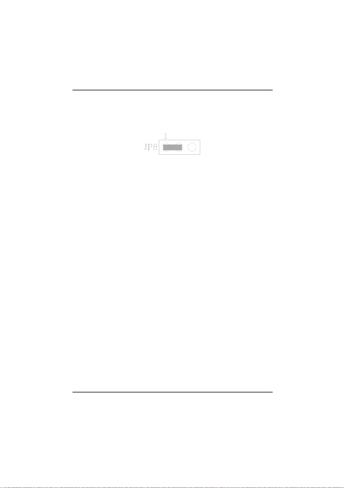
2.7 JP8 - CLEAR CMOS DATA 15
2.8 JP1 - VOLTAGE SELECTION FOR SYSTEM ROM 16
2.9 JP3 - ONBOARD AUDIO SELECT 17
2.10 JP4, 5 - ONBOARD VGA SELECT 17
2.11 RESERVED JUMPERS 17
2.12 MEMORY CONFIGURATION 18
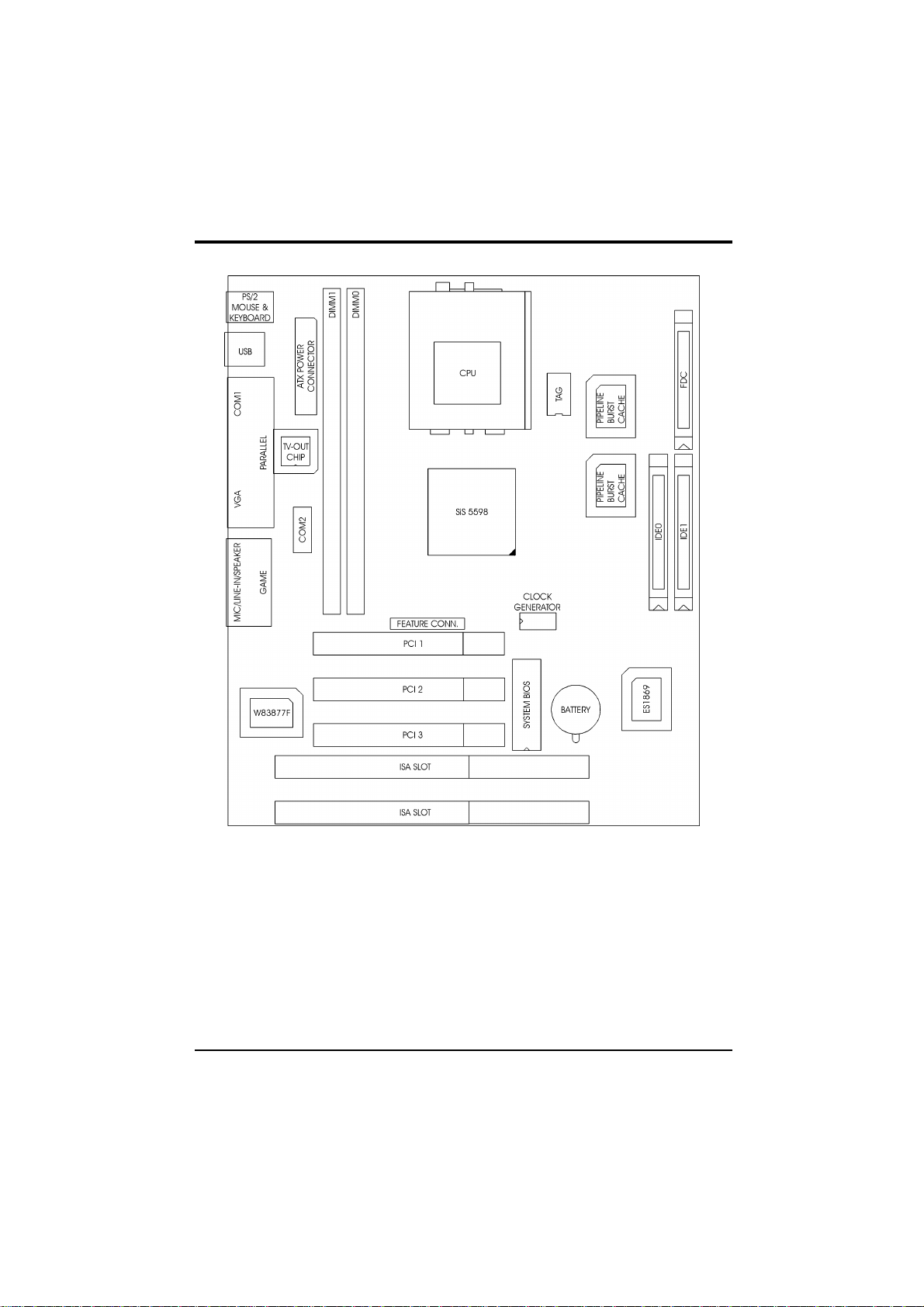
CHAPTER 3 CONNECTOR CONFIGURATION 19
3.1 J1 - MULTIPLE FUNCTION JUMPER 20
3.2 J3 - CD-ROM AUDIO CONNECTOR (MISUMI/PANASONIC) 20
3.3 J4 - CD-ROM AUDIO CONNECTOR (SONY) 21
3.4 J5 - FLOPPY DRIVE CONNECTOR 21
3.5 J6, J7 - PRIMARY/SECONDARY IDE CONNECTORS 21
3.6 J8 - IrDA/FAST IR CONNECTOR 21
3.7 JP9 - INTERNAL MODEM RING-IN CONNECTOR 22
3.8 J10 - FEATURE CONNECTOR 22
3.9 J11 - SERIAL PORT COM2 CONNECTOR 22
3.10 J16 - ATX POWER CONNECTOR 22
3.11 J17 - CPU FAN CONNECTOR 23
3.12 J18 – TV OUT CONNECTOR 23
3.13 PS/2 KEYBOARD CONNECTOR 24
3.14 PS/2 MOUSE CONNECTOR 24
3.15 UNIVERSAL SERIAL BUS PORTS 0 & 1 24
3.16 PARALLEL PORT CONNECTOR 24
3.17 SERIAL PORT COM1 24
3.18 AUDIO PORT CONNECTOR 25

III
CHAPTER 4 AWARD BIOS SETUP GUIDE 27
4.1 AWARD BIOS SETUP 27
4.2 STANDARD CMOS SETUP 29
4.3 BIOS FEATURES SETUP 30
4.4 CHIPSET FEATURES SETUP 32
4.5 POWER MANAGEMENT SETUP MENU 33
4.6 PCI CONFIGURATION 35
4.7 INTEGRATED PERIPHERALS SETUP MENU 36
4.8 LOAD SETUP DEFAULTS MENU 38
4.9 SUPERVISOR PASSWORD 38
4.10 USER PASSWORD 39
4.11 IDE HDD AUTO DETECTION 39
4.12 SCSI HARD DISK INSTALLATION 40
4.13 SAVE & EXIT SETUP MENU 40
4.14 EXIT WITHOUT SAVING MENU 40
CHAPTER 5 SOFTWARE INSTALLATION 41
5.1 PCI IDE DRIVER INSTALLATION 41
5.2 PCI VGA DRIVER INSTALLATION 41
5.3 SOUND DRIVER INSTALLATION 41
5.4 THE AUDIORACK32 FOR WIN95 42
5.4.1 INTRODUCTION 42
5.4.2 INSTALLING THE AudioRack32 42
5.4.3 UNINSTALLING THE AudioRack32 45
5.5 XING MPEG PLAYER (OPTIONAL) 45
CHAPTER 6 AWARD ZERO-VOLT DATA-SUSPEND UTILITY 47
6.1 INTRODUCTION 47
6.2 PREPARATION 47
6.3 RUNNING THE PROGRAM 48
6.3.1 INSTALLATION 48
6.3.2 SAVING SESSION DATA 50
6.4 PROGRAM FUNCTIONS 51
6.4.1 USAGE 51
6.4.2 REFORMATTING THE STORAGE PARTITION 52
6.4.3 DELETING THE STORAGE FILE OR PARTITION 52
CHAPTER 7 FLASH AND DMI UTILITY 53
7.1 AWARD FLASH UTILITY 53
7.2 DESKTOP MANAGEMENT INTERFACE (DMI) OVERVIEW 55
APPENDIX A QUICK GUIDE 59


1
CHAPTER 1 INTRODUCTION
Preface
The motherboard is a full ATX form factor high performance all in one mainboard. It is
developed around the pentium microprocessor with 64 bit access to data transfer and MMX
technology. It includes SiS 5598 PCI/ISA System Chipset with Graphics/Video accelerate
function build-in, Winbond W83877F super I/O chip, ESS 1869 Sound System.
Features
Processor
•Intel Pentium/MMX, Cyrix 6x86/6x86L/6x86MX/M II and AMD K5/K6/K6-2 and IDT C6
CPU.
•The mainboard can run with following speeds:
90, 100, 110, 120, 133, 150, 166, 200, 233, 250, 266, 300 and 333MHz
Chipset
•SiS 5598 PCI, Memory and VGA Controller
•Winbond W83877F Super I/O Controller
•ESS 1869 Audio-Drive Sound Controller
Cache Size
•Built in 512KB Synchronised Pipelined Burst Mode SRAM to achieve the high Pentium
system performance.
Main Memory
•Support Mixed Memory Technologies: Extend Data Output (EDO) and Synchronous
DRAM (SDRAM) can work together.
•Memory configurations from 8MB to 256MB using 2M*32 to 8M*32 SDRAM DIMM
module.
•DIMM socket for SDRAM/EDO (3.3V unbuffered).
Graphics Controller
•Built-in an enhanced 64-bit BITBLT graphics engine with VGA feature connector on board.
•PCI 2.1 compliance and PCI multimedia design Rev 1.0 support.
•Support DCI Drivers and Direct Draw Drivers.
TV-OUT
•TrueScalerendering engine supports underscan operation for both 640x480 or 800x600
inputs
•Supports both NTSC and PAL (B,D,G,H or I) TV formats onto both composite and S-video
(option).

Chapter 1
2
Fig. 1 Key Components of the Mainboard

Introduction
3
Multi I/O
•On board Multi-I/O supports two serial, one parallel ports and floppy drive controller.
•Serial ports are 16550 Fast UART compatible.
•Parallel port has EPP and ECP capabilities.
•PS/2 keyboard and PS/2 mouse connector is provided.
•IrDA or Fast IR is provided.
•Two standard USB connectors are provided.
PCI IDE
•On board supports PCI Master IDE Controller, two connectors support up to four IDE
devices such as HDD, CD ROM drive and Tape Back-up drives LS-120, etc.
•PCI Master IDE controller supports PIO Mode 3 and 4 devices, I/O data transfer rate can be
up to 17Mb/s.
•Ultra DMA Mode supported. Transfer rate can be up to 33MB/s.
Sound Controller
•Compatible with all major PC sound standards, including Sound BlasterPro, MPU-401
and Windows Sound System.
•Plug-and-Play support for Audio, Joystick, FM Controller, MPU-401.
•Wave Audio support sample rates from 4KHz to 44KHz.
•Full-duplex monophonic mode, half-duplex stereo mode.
•3D stereo sound effect supported.
•Optional wavetable connector is provided.
System BIOS
•Award BIOS (256KB Flash EPROM).
Slots
•Three PCI slots
•Two ISA slots
Form Factor
•245mm (W) x 210mm (L) 4 Layer

Chapter 1
4
Environment
Working Specifications
Actual Field MTBF (hours) 104,515 hours
Preventive Maintenance Not Required
Environmental Limits Operating Non-operating
Temperature 0 to 50 degree Celsius -10 to 65 Degree Celsius
Relative Humidity
(without condensation) 8 to 85% 5 to 95%
Altitude 10,000ft 40,000ft
Vibration 1,000Hz
Electricity 4.75 ∼5.25V

5
CHAPTER 2 JUMPER SETTINGS
2.1 JUMPERS PRESENTATION
Pins 1 and 2 are shorted with a jumper cap.
1 2 3
Pins 2 and 3 are shorted with a jumper cap.
1 2 3
The jumper is shorted when the jumper cap is placed
over the two pins of the jumper.
The jumper is open when the jumper cap is removed
from jumper.
2.2 CPU TYPE
2.2.1 INTEL PENTIUM CPU
The pentium processors have different operation voltage. In order to using the CPU
Voltage correctly, the following is the marking for identify the CPU type.
Fig. 2a CPU Description
(Bottom Side)
Description :
X = Voltage Specification (S or V) Y = Timing Specification (S or M)
S = Standard Voltage (3.4V) S = Standard EDS timings
V = VRE 3.4 - 3.6V (3.5V) M = Min Valid Delay Spec.
Z = Dual Processing Support ( S or U)
S = Support DP/MP/UP
U = Not tested to support DP

Chapter 2
6
2.2.2 INTEL PENTIUM w/ MMX TECH (P55C) CPU
The Intel Pentium w/ MMXTech (P55C) CPU is offered with dual voltage supply
- 2.8V for core and 3.3V (I/O) interface. The following is the marking for identify
the CPU type. (The following diagram is provided as an example only. It does not
necessarily indicate a valid product marking.)
Fig. 2b CPU Description
(Top Side)
2.2.3 AMD-K6 CPU
The AMD-K6 CPU family requires dual voltage power for operation. The AMD-
K6/166, 200 require a voltage of 2.9V core and 3.3V I/O. The AMD-K6/233
requires a voltage of 3.2V core and 3.3V I/O. The AMD-K6/266, 300 require a
voltage of 2.2V core and 3.3V I/O. (The following diagram is provided as an
example only. It does not necessarily indicate a valid product marking.)
Fig. 2c CPU Description
(Top Side)
Operating Voltage I/O Voltage Core Voltage
2.2V 3.3V 2.2V
2.9V 3.3V 2.9V
3.2V 3.3V 3.2V

Jumper Settings
7
2.2.4 AMD-K5 CPU
The AMD-K5 family CPU operates on different operation voltage depending on the
CPU type. The operating voltage can be known through the marking on the surface of
the CPU. (The following diagram is provided as an example only. It does not
necessarily indicate a valid product marking.)
Fig. 2d CPU Description
(Top Side)
2.2.5 CYRIX 6x86 CPU
The Cyrix 6x86 has different nominal voltage depends on different lot. Please refer to
the CPU marking.
Fig. 2e CPU Description
(Top Side)
Marketing Recommended Nominal Voltage
3.3V or 3.52V 3.52V
028 3.52V
016 3.3V
Blank 3.52V

Chapter 2
8
2.2.6 CYRIX 6x86L CPU
The Cyrix 6x86L has different I/O and core voltage. Please refer to the CPU
marking.
Fig. 2f CPU Description
(Top Side)
2.2.7 CYRIX 6x86MX CPU
The Cyrix 6x86MX has different I/O and Core Voltage. Please refer to the CPU
marking.
Fig. 2g CPU Description
(Top Side)
I/O Voltage Core Voltage
Cyrix 6x86MX 3.3V 2.9V
Cyrix 6x86L 3.3V 2.8V

Jumper Settings
9
2.2.8 IDT WinCHIP C6 CPU
The IDT WinChip C6 CPU has different operating voltage. Please refer to the CPU
marking to identify the operating voltage.
Fig. 2h CPU Description

Chapter 2
10
2.3 GRAPHICAL DESCRIPTION OF JUMPER
SETTINGS
Fig. 3 Jumper Location of the mainboard

Jumper Settings
11
2.4 CPU VOLTAGE
2.4.1 CPU VOLTAGE BIOS SELECTION
The CPU Voltage can be selected through BIOS setup “CPU Core Voltage
Selection”. It can be set as following table:
2.2 AMD K6 (2.2V)/K6-2
2.8 Intel MMX (P55C); Cyrix 6x86L
2.9 AMD K6 (2.9V); Cyrix 6x86MX/M II; IBM 6x86MX
3.2 AMD K6 (3.2V)
3.3 Intel Pentium
3.52 Cyrix 6x86; AMD K5, IDT WinChip
Table 1

Chapter 2
12
2.4.2 CPU VOLTAGE MANUAL SELECTION
The CPU Core Voltage can be selected by SW1-1, 2, 3 and 4.
Voltage SW1 JP2 S1 CPU Type
2.2V AMD K6 (2.2V)/K6-2
2.8V Intel Pentium w/MMX (P55C);
Cyrix 6x86L
2.9V AMD K6 (2.9V);
Cyrix 6x86MX/M II;
IBM 6x86MX
3.2V AMD K6 (3.2V)
3.3V Intel Pentium (P54C)
3.5V 6x86; AMD K5; IDT WinChip
Table 2
ON
1 2 3 4
ON
1 2 3 4
ON
1 2 3 4
ON
1 2 3 4
ON
1 2 3 4
ON
1 2 3 4

Jumper Settings
13
2.5 CPU TO BUS FREQUENCY RATIO (SW1-5,6,7)
These jumpers set the frequency ratio between the Internal frequency of the CPU and
the External frequency (called the Bus clock) within the CPU. These must be set
together with the above jumpers CPU External (Bus) Frequency Selection.
2.6 CPU EXTERNAL (BUS) FREQUENCY SELECTION
(SW1-8,9,10)
These switches tell the clock generator what frequency to send to the CPU. The Bus
clock times the Bus Ratio equals the CPU’s Internal frequency.
Fig 5
CPU Type Freq. Ratio Bus Ratio Setting Bus Freq. Setting
Freq. SW1-5 SW1-6 SW1-7 SW1-8 SW1-9 SW1-10
Intel Pentium 90MHz 1.5x 60MHz OFF OFF OFF ON OFF OFF
Intel Pentium 100MHz 1.5x 66MHz OFF OFF OFF OFF OFF OFF
Intel Pentium 120MHz 2.0x 60MHz ON OFF OFF ON OFF OFF
Intel Pentium 133MHz 2.0x 66MHz ON OFF OFF OFF OFF OFF
Intel Pentium 150MHz 2.5x 60MHz ON ON OFF ON OFF OFF
Intel Pentium 166MHz 2.5x 66MHz ON ON OFF OFF OFF OFF
Intel Pentium 200MHz 3.0x 66MHz OFF ON OFF OFF OFF OFF
Intel Pentium w/MMX 166MHz 2.5x 66MHz ON ON OFF OFF OFF OFF
Intel Pentium w/MMX 200MHz 3.0x 66MHz OFF ON OFF OFF OFF OFF
Intel Pentium w/MMX 233MHz 3.5x 66MHz OFF OFF OFF OFF OFF OFF
AMD-K5-PR120 120MHz 2.0x 60MHz ON OFF OFF ON OFF OFF
AMD-K5-PR133 133MHz 2.0x 66MHz ON OFF OFF OFF OFF OFF
AMD-K5-PR166 166MHz 2.5x 66MHz ON ON OFF OFF OFF OFF
AMD-K6/166 166MHz 2.5x 66MHz ON ON OFF OFF OFF OFF
AMD-K6/200 200MHz 3.0x 66MHz OFF ON OFF OFF OFF OFF
AMD-K6/233 233MHz 3.5x 66MHz OFF OFF OFF OFF OFF OFF
AMD-K6/266 266MHz 4.0x 66MHz ON OFF ON OFF OFF OFF
AMD-K6-2/266 266MHz 4.0x 66MHz ON OFF ON OFF OFF OFF
AMD-K6/300 300MHz 4.5x 66MHz ON ON ON OFF OFF OFF
To be continued…
Table 3a
ON
5 6 7 8 9 10

Chapter 2
14
CPU Type Freq. Ratio Bus Ratio Setting Bus Freq. Setting
Freq. SW1-5 SW1-6 SW1-7 SW1-8 SW1-9 SW1-10
Cyrix 6x86L-PR150 120MHz 2.0x 60MHz ON OFF OFF ON OFF OFF
Cyrix 6x86L-PR166 133MHz 2.0x 66MHz ON OFF OFF OFF OFF OFF
Cyrix 6x86L-PR200 150MHz 2.0x 75MHz ON OFF OFF OFF ON ON
Cyrix 6x86MX-PR166 150MHz 2.5x 60MHz ON ON OFF ON OFF OFF
Cyrix 6x86MX-PR200 150MHz 2.0x 75MHz ON OFF OFF OFF ON ON
Cyrix 6x86MX-PR200 166MHz 2.5x 66MHz ON ON OFF OFF OFF OFF
Cyrix 6x86MX-PR233 188MHz 2.5x 75MHz ON ON OFF OFF ON ON
Cyrix 6x86MX-PR233 200MHz 3.0x 66MHz OFF ON OFF OFF OFF OFF
Cyrix M II-300 225MHz 3.0x 75MHz OFF ON OFF OFF ON ON
Cyrix M II-300 233MHz 3.5x 66MHz OFF OFF OFF OFF OFF OFF
IDT WinChip C6-180 180MHz 3.0x 60MHz OFF ON OFF ON OFF OFF
IDT WinChip C6-200 200MHz 3.0x 66MHz OFF ON OFF OFF OFF OFF
IBM 6x86MX-PR266 208MHz 2.5x 83MHz ON ON OFF ON ON ON
IBM 6x86MX-PR300 225MHz 3.0x 75MHz OFF ON OFF OFF ON ON
IBM 6x86MX-PR300 233MHz 3.5x 66MHz OFF OFF OFF OFF OFF OFF
IBM 6x86MX-PR333 250MHz 3.0x 83MHz OFF ON OFF ON ON ON
Table 3b
This manual suits for next models
1
Table of contents
Other DTK Motherboard manuals