DTK PIM-TB10-Z User manual

PIM- TB 10-2
10MHz Mainboard
User Manual

PIM- TB 10-2
10MHz Mainboard
User Manual
Edition 1.02
©1989 Datatech Enterprises Co., Ltd.
This manual and the PlM-TBtO-Z mainboard are copyrighted with all
rights reserved. Under the copyright laws, neither this manual nor the
PIM-TB10-Z mainboard may be copied, in whole or in pan, without the
express written consent of Datatech Enterprises Co., Ltd.

Checklist
Your PlM-TBtO—Z package contains the following:
-One PlM-TBtO—Z mainboard
-One PlM-TBt O—Z user manual
The following does not apply to any country where such provisions are
inconsistent with local law:
Datatech makes no warranties with respect to this documentation
either express or implied and provides it "as is". This includes but is not
limited to any implied warranties of merchantability and fitness for a
particular purpose. The information in this document is subject to
change without notice. Datatech assumes no responsibility for any
errors that may appear in this document.
lBM, IBM PC and PC/XT are registered trademarks of International
Business Machines Corporation. The typeface used in the text of this
manual is 12 point Helvetica and is used under licence from the Allied
Corporation, the owner of the typefaces
)

Con tents
Introduction &Features..........................................
1
Board layout ................................................................ 2
Installation....................................................................3- 15
RAM installation &configuration ................................ 3-4
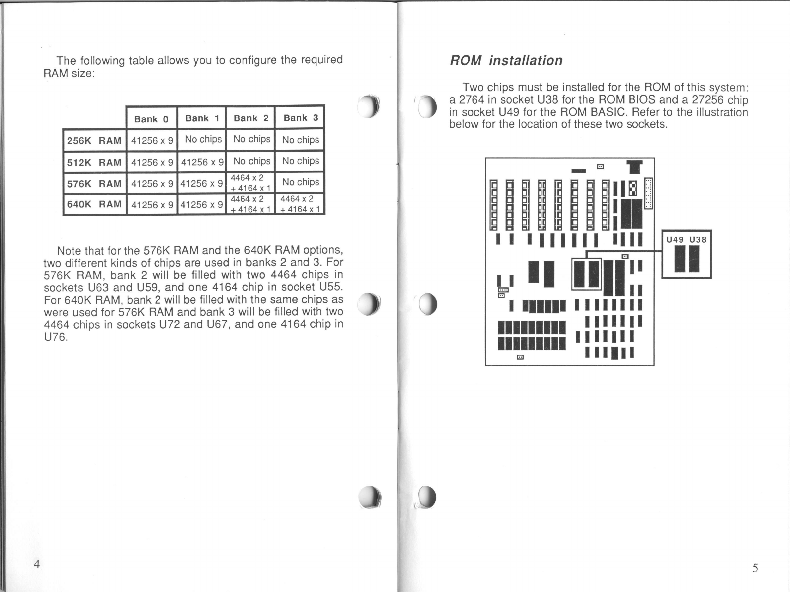
ROM installation ....................................................... 5
DIP switch settings ................................................... 6-8
Panel indicators and switches ....................................
9-10
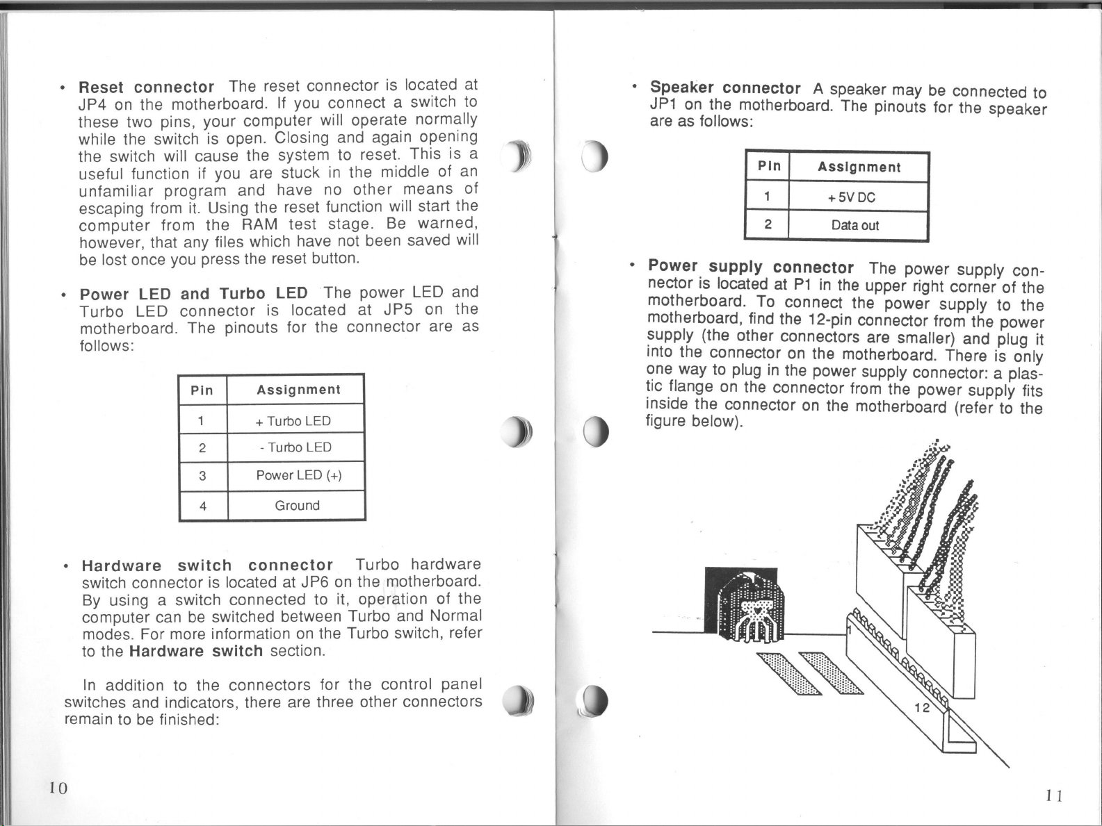
Speaker and power supply connector......... ....11-12
Keyboard connector................................................. 13
Fastening motherboard to case ................................. 14-15
Reconfiguring.............................................................. 16
Operation ...................................................................... 17-20
Obtaining 10MHz Turbo mode .................................. 18
Setting default operation mode ................................. 18
Software switch ........................................................ 18-19
Hardware switch ....................................................... 19
Alternate use of both switches .................................. 20
Turbo LED and hardware switch ................................ 20
Technical information ............................................. 21 -30
Introduction ............................................................. 21-22
DMA........................................................................ 22
Timer....................................................................... 22
Interrupt ................................................................... 23
Memory ................................................................... 23
Keyboard ................................................................. 23
Speaker ................................................................... 24
Expansion I/O channel..............................................24-25
I/O channel description ............................................. 26—29
Speaker interface ..................................................... 30
1
)
J.9
Introduction
You can rest assured of having made awise choice in
buying the PIM-TB10-Z motherboard for your personal
computer. This motherboard is not only compatible with
the PC/XT but provides you with these features:
-16-bit 8088-10 CPU or qualified 8088-2 CPU (optional
8087-1 coprocessor).
-Switchable processing speed in 10MHz (110% faster
than normal —4.77MHz) and 4.77MHz.
-Turbo/Normal modes selectable by either asoftware
switch or ahardware switch.
-Memory expandable to 640K on mainboard.
-ROM capacity —8K BIOS.
~LEGAL BIOS from ERSO (Electronics Research &
Organization),
8expansion slots.
4-channel DMA for disk and special I/O.
3-channel timer for music and time.
8-Ievel interrupt.
-IBM PC/XT® compatible.
-Operating systems :MS-DOS®, CPM/86®, CCP/M®.
-Speed test
by Norton® Utility :2.1
by Landmark® Speed Test Program :4.1
The clear, well-illustrated instructions in this manual
ensure that even if you are a newcomer to the computer
world, you will have your system installed and running
with the minimum of effort.

Board Iagut
'''"''th the layout
he Illustration below WI” familiarize you WI
_
of She PlM-TBtO—Z motherboard and Its onboard Jumpers.
=2“
'l
EEEEEE’E-u—
l
JP5—
JP8- ull II
fl
—El IIIIIII III
IIIIIIIII ”
IIIIIIIII
?
B——JP3
I
JP1
Installation
RAM installation
Four kinds of RAM size are possible with the PlM-TBtO-
Zmotherboard. The figure below shows the location of the
RAM banks. Remember that when inserting chips in their
sockets, you must make sure that the notched end of the
chip is lined up with the notched end of the socket.
E
I“
II
E” II
Bank 3Bank 2
iliili
‘IIIIIIIlI
Bank 1
\
K-
WIIIIIIIII
‘

The following table allows you to configure the required
RAM size:
Bank 0Bank 1Bank 2Bank 3
256K RAM 41256 X9Nocmps Nochms No chips
512K RAM 41256 X941256 X9Nochms Nocmps
576K RAM 41256x9 41256 X94464x2
+4164x1 Nocmps
640K RAM 41256 X941256 X94464X2
+4164X1
4464X2
+4164X1
Note that for the 576K RAM and the 640K RAM options,
two different kinds of chips are used in banks 2and 3. For
576K RAM, bank 2will be filled with two 4464 chips in
sockets U63 and U59, and one 4164 chip in socket U55.
For 640K RAM, bank 2will be filled with the same chips as
were used for 576K RAM and bank 3will be filled with two
4464 chips in sockets U72 and U67, and one 4164 chip in
U76.
ROM installation
Two chips must be installed for the ROM of this system:
a2764 in socket U38 for the ROM BIOS and a27256 chip
in socket U49 for the ROM BASIC. Refer to the illustration
below for the location of these two sockets.
U49 U38
LEIIIIIIIIIIIIIII
lIlIIIIII "'”"
IIII
Illl
IIIEIIIII ml”
_
':_E§l

DIP switch settings
DIP switch SW1 is used to set the system configuration.
For the location of the switch and the settings, refer to the
following illustrations:
SW1
1-ON
2-
3-
4-
5-
6-
7-
8-
|I3‘
IIE.
II:1
IIL
IIa
II!_
III
I
E
II II '
lgw' Ill
IIIIIIIIIIIIII
IIIIIIIII ""”
IIIIIIIII "'""
ca IIIIII
9
0N
H| | | || | |normal operation
12 3 4567 8
ON ..
operation wrthout 8087
E9 5EE E E 5coprocessor
ON ..
operation With 8087
!E E !g g g Ecoprocessor
ON for enhanced graphics
IIIIEEl I I
12345678 adapter
ON for color graphics
IIIIHHII adapter(40x20
12345678 mOde)
0N for color graphics
IIIIllliilll adapter(80x25
12345678 mode)
NOTE:
5indicates SW on
Hindicates SW off

—————-r-——‘
(Continued) .Panel indicators and switches
How you attach the mainboard to the case of your
0” for monochrome ~system unit is fairly up to you. This is because the PIM-
II Ill HIIdisplay adapter w)TBtO-Z Turbo mainboard can be used in avariety of
1234567880286-type system unit cases.
Under typical conditions, your system unit will have all
ON the indicators and switches shown below and preferably
IIIIIIEHfor one disk drive even areset switch, aTurbo hardware switch and aTurbo
123 4 5s7a'LED. If not, you can either install anew panel display or
omit some of these items from your system. Your computer
dealer offers an accessory which allows you to add the
ON
--two switches and the LED to your system. An example of
!!!!!!E Efor two dlSk dnves an "ideal" display panel for your computer is pictured
below:
ON
IIIIIIuufor three disk drives
12 3 45678
ON )ll l)
||| | ||nHfor four disk drives
12345678
Functions of panel indicators and switches
The PlM-TBtO-Z motherboard provides the following
connectors for your control panel:
.Keylock connector The keylock connector is located
at JP3 on the motherboard. By using akeylock device
on your control panel to put the two pins at JP3 in a
closed circuit, the keyboard is unlocked. When the two
pins are in an open circuit, the keyboard is locked.
Jill)

Reset connector The reset connector is located at
JP4 on the motherboard. if you connect aswitch to
these two pins, your computer will operate normally
while the switch is open. Closing and again opening
the switch will cause the system to reset. This is a
useful function if you are stuck in the middle of an
unfamiliar program and have no other means of
escaping from it. Using the reset function will start the
computer from the RAM test stage. Be warned,
however, that any files which have not been saved will
be lost once you press the reset button.
Power LED and Turbo LED The power LED and
Turbo LED connector is located at JP5 on the
motherboard. The pinouts for the connector are as
follows:
Pin Assignment
1+Turbo LED
2-Turbo LED
3Power LED (+)
4Ground
Hardware switch connector Turbo hardware
switch connector is located at JP6 on the motherboard.
By using aswitch connected to it, operation of the
computer can be switched between Turbo and Normal
modes. For more information on the Turbo switch, refer
to the Hardware switch section.
In addition to the connectors for the control panel
-Speaker connector Aspeaker may be connected to
JP1 on the motherboard. The pinouts for the speaker
are as follows:
Pln Assignment
1+5V DC
2Data out
Power. supply connector The power supply con-
nector IS located at P1 in the upper right corner of the
motherboard. To connect the power supply to the
motherboard, find the 12-pin connector from the power
supply (the other connectors are smaller) and plug it
into the connector on the motherboard. There is only
one way to plug in the power supply connector: aplas—
tic flange on the connector from the power supply fits
msrde the connector on the motherboard (refer to the
figure below).
switches and indicators, there are three other connectors J) 9
remain to be finished: ‘(
11

The pinouts for the power supply connector are as
shown below:
Pin Assignment
1Power good
Not used
+12V DC
-12V DC
Ground
Ground
Ground
Ground
mmVQU'I-uww
-5V DC
+5V DC
.1» O
11 +5VDC
12 +5VDC
l12
.Keyboard connector The keyboard connector is
located at the back of your system unit as shown in the
figure below:
Location of keyboard connector
from back panel
The keyboard connector is afive-pin DIN connector.
The pinouts are give below:
Pin Assignments
1Keyboard clock
2Keyboard data
3Spare
4Ground
5+5 VDC
13

Fastening motherboard to case
Open the case of your system unit. if it is an empty case,
it should look something like the illustration below:
Notice the two types of fastening points circled. The
slots may be used with plastic connectors inserted into the
motherboard, or brass female connectors. Brass female
connectors will be screwed into the holes in the case. The
plastic and brass connectors are pictured below:
Brass &Plastic
V
connector Iconnector
@
W
14
Screw the brass connectors into the case as shown
below:
\)Base of
‘
.case
Insert the plastic connectors into the holes on the
motherboard which will be located above the slot-type
connectors in your case. The pointed ends of the plastic
connectors should be on the top side of the motherboard.
0Note that using the plastic connectors is optional, but
you should use the brass connectors in order to ground
the motherboard to your case. if you have used the plastic
connectors in the motherboard, slide them into the slots in
the case. Next, fasten the motherboard to the brass
connectors with screws. Otherwise, simply place the
motherboard over the brass connectors in the case and
screw the motherboard snugly down to them.
The motherboard is now fastened to the case.
.0
15

Reconfiguring
“Warning
To ensure the reliability of the computer, NEVER
reconfigure the board while the power is ON.
If you wish to reconfigure the system board at any time,
ensure that the power to the system is turned OFF before
changing any hardware settings, such as DIP switches or
jumpers.
16.
1
Operation
The main advantage of the PlM-TB10-Z Turbo mother-
board over ordinary PC/XT motherboards is its dual clock
system. This innovation makes it possible for your com-
puter to operate at either of two clock speeds: 4.77MHz or
10MHz. In the 10MHz Turbo mode, your computer will op-
erate up to 110% faster than aconventional 8088-based
computer.
NOTE: Do not use RAM memory on an expansion card
because its design may not be compatible with the 1OMHz
CPU at access time. Use memory on the motherboard
comprised of 4164 and 41256 and 4464 chips within
120ns. Refer to RAM installation section. Recom-
mended chips are shown in the table below.
4164 41256 4464
NEC D4164C D412560 D4464C
Hitachi HM4846 HM50256 HM50464
Mitsubishi M5K4164 M5M4256P M5M4464P
Panasonic MN4164 MN41256 MN4464
NOTE: Use NEC® 70108-10 chips to achieve speeds up
to 380% faster than an ordinary XT.
17

Obtaining 10MHz Turbo mode
This mainboard supports both asoftware switch and a
hardware switch for changes between Normal and Turbo
modes.
Setting default operation mode
The Turbo hardware switch, jumper JP6 (shown on
page 3), gives you the choice of running the PlM-TBtO-Z
in either Normal or Turbo mode when the power is on. For
default operation:
-In Normal mode ..... Place ajumper cap over JP6
.ln Turbo mode ....... Take the jumper cap off JP6
Software switch
Before using the software switch, pay attention to
whether default operation is in Normal or Turbo mode. If it
is in Normal mode, do the following: press and hold down
the control <Ctrl >and alternate <Alt >keys on the
keyboard while you press the minus <-> key. The cursor
on the screen will turn into abox. The Turbo LED on your
panel, if you have installed one, will light. For more
information on the Turbo LED, refer to the Panel
indicators and switches section. Now the computer is
in Turbo mode.
To return to Normal mode, press the same keys you
used to enter Turbo mode. When you enter Normal mode,
the cursor will return to the dash (_ )form and the Turbo
LED will turn off.
18
3
0
If default operation is in Turbo mode, press and hold
down the control <Ctrl >and alternate <Alt >keys on the
keyboard while you press the minus <->key to go to
Normal mode. The Turbo LED will turn off, and the cursor
will turn into abox. To return to Turbo, press the same
keys: the Turbo LED will light and the cursor will change
into adash.
Hardware switch
if you have ahardware switch on your panel, connect it
to jumper JP6. More information on this is given in the
Panel indicators and switches section.
Push the hardware switch on to enter Normal mode
and push it off to enter Turbo mode.
___
Hardware switch off ___
Hardware switch on
Using the hardware switch means that the only
indication of the mode your computer is in will be the
Turbo LED. It will turn on in the Turbo mode and turn off in
the Normal mode. The cursor will always have the same
appearance.
19

Alternate use of both switches
Both the hardware and the software switches may be
used alternatively, but this is not advised because you
may become confused about the mode of operation.
When using both switches alternatively, the Turbo LED
will be the only accurate indicator of the actual mode: the
LED will be on in Turbo mode and off in Normal mode.
Turbo LED and hardware switch
Most 8088—type computer cases do not have aTurbo
LED or aTurbo hardware switch. However, both of these
items are very useful as you probably can already see.
Therefore, it is highly recommended that you install both
in your system if you do not already have them. For more
information, refer to the Panel indicators and
switches section.
Using software in Turbo made
Most software, such as Lotus 1-2-3®, dBase lll® and
many other applications run flawlessly in Turbo mode.
However, you may find that certain kinds of software, like
Copy Writer®, runs only in Normal mode.
20
Technical information
The system board is adouble-sided printed circuit
board using direct current. The power supply is connected
to the board by a12—pin connector. Other connectors are
for acontrol panel, aspeaker and akeyboard. Eight 62-
pin expansion slots are also mounted on the board. The
l/O channel'
Is bussed across these eight l/O slots.
An eight-
-switch Dual— In- Line Package (DlP) switch
(SW1) is mounted on the board and can be read under
program control. The DIP switch provides the system soft-
ware with information about the installed options, how
much storage the system has, what type of display
adapter is installed, what operation modes are desired
when power is switched on (c
color or black and white, 80-
or 40-character lines) and the number of diskette drives
anached.
The system board had five functions: the processor
subsystem and its support elements, the Read Only Mem-
ory (ROM) subsystem, the ReadNVrite (RNV) Memory sub-
system, the integrated l/O adapters and the l/O channel.
The heart of the 10MHz Turbo system board is the
Intel® 8088-1 microprocessor. This processor is an 8—bit
external bus version of Intel®'s 16-bit 8086 processor and
is software-compatible with the 8086. Thus, the 8088 sup-
ports 16-bit operations including multiply and divide and
supports 20 bits of addressable memory (1 megabyte of
storage).
21

It also operates in amaximum mode so acoprocessor
can be added as a feature. The processor operate in two
modes which can be switched, namely the Normal mode
and the Turbo mode. When the processor is operating in
Normal mode (4.77MHz), the frequency which is derived
from a14.318MHz crystal, is divided by three for the pro—
cessor clock, and by 4to obtain the 3.58MH2 color burts
signal required for color television. When the processor is
operating in Turbo mode (10MHz), the frequency is de-
rived from 30MHz. ,
DMA
Three of the four DMA channels are available on the l/O
bus and support high-speed data transfers between l/O
devices and memory without processor intervention. The
fourth DMA channel is programmed to refresh the system
dynamic memory. This is done by programming achannel
of the timer counter device to request periodically a
dummy DMA transfer. This action creates amemory-read
cycle which is available to refresh dynamic storage both
on the system board and expansion slots. All DMA data
transfers except the refresh channel take five processor
clocks of 210ns or 1.05us if the processor ready line is not
deactivated. Refreshing DMA cycles takes four clocks
(840ns).
Timer
The three programmable timer/counters are used by
the system as follows: Channel 0is used as a general-
purpose timer providing a constant time base for
implementing atime-of—day clock; Channel 1is used to
time and request refresh cycles from the DMA channel;
and Channel 2is used to support the tone generation for
the audio speaker. Each channel has aminimum timing
resolution of 1.05us.
22
0
O
Interrupt
Of the eight prioritized levels of interrupts, six are
bussed to the expansion slots for use by the interface
cards. Two levels are used on the system board. Level 0,
the highest priority, is attached to Channel 0 of the
timer/counter and provides aperiodic interrupt for the
time-of-day clock. Level 1is attached to the keyboard
adapter circuits and receives an interrupt for each scan
code sent by the keyboard. The Non—Maskable Interrupt
(NMI) of the 8088 is used to report memory-parity errors.
Memory
The system board supports both ROM/EPROM and FWV
memory. It has space for 32KB x1and 8KB x1of ROM or
EPROM. This ROM contains apower-on self—test, l/O
drivers, dot patterns for 128 characters in graphics mode
and adiskette. The system board also has from 256KB to
640KB of RM memory. Aminimum system has 256KB of
memory.
Keyboard
The system board contains the adapter circuits for
attaching the serial interface from the keyboard. These
circuits generate an interrupt to the processor when a
complete scan code is received. The interface can request
execution of adiagnostic test in the keyboard. The
keyboard interface is afive-pin DIN connector on the
system board that extends through the rear panel of the
system unit.
23

Speaker
The system unit has a21/4-inch audio speaker. The
speaker's control circuits and driver are on the system
board. The speaker connects through a two-wire interface
that attached to athree-pin connector on the system
board. The speaker drive circuit is capable of providing
approximately 1/2 watt of power. The control circuits allow
the speaker to be driven three different ways:
0Adirect program control register bit may be toggled to
generate apulse train.
-The output from Channel 2of the timer/counter may be
programmed to generate awaveform to the speaker.
0The clock input of the timer/counter can be modulated
with aprogram controlled by the I/O register bit. All
three methods may be performed simultaneously.
Expansion [/0 channel
The l/O channel is an extension of the 8088 micropro-
cessor bus. It is, however, demultiplexed, repowered and
enhanced by the addition of interrupts and Direct Memory
Access (DMA) functions.
The l/O channel contains an 8-bit, bidirectional data
bus with 20 address lines, six levels of interrupt, control
lines for memory and l/O read or write, clock and timing
lines, three channels of DMA control lines, memory
refresh timing control lines, achannel check line, apower
line and aground for the adapters. Four voltage levels are
provided for the expansion cards: +5V DC, -5V DC, +12V
DC and -12V DC. These functions are provided in a62-
pin connector with too-mil card tab spacing.
24
0
O
A"ready" line is available on the l/O channel to allow
operation with slow I/O or memory deVIces. If the
channel's ready line is not activated by an addressed
device, all processor-generated memory read and write
cycles take four 210ns/clock or 840ns/byte. All processor—
generated l/O read and write cycles reqUIre five clocks for
acycle time of 1.05us/byte. Refresh cycles occur once
every 72 clocks (approximately 15us) andrequne four
clocks or approximately 7% of the bus bandWIdth.
l/O devices are addressed using l/O-mapped space.
The channel is designed so that 768 l/O devnces
addressed are available to the l/O expansion cards.
Achannel check line exists for reporting error
conditions to the processor. Activating this line results in a
Non-Masksable Interrupt (NMI) to the 8088 processor.
Memory expansion options use this line to report parity
errors.
The l/O channel is repowered to provide sufficient drive
to power all eight (J1 through J8) expansion slots, under
conditions of two Low-power Schottsky (LS) loads per
slot. The l/O adapters typically use only one load.

[/0 channel description
The following is adescription of the PC/XT l/O channel.
All lines are TTL compatible.
OSC, oscillator
It is ahigh-speed clock with a70ns period
(14.31818MHz). It has a50% duty cycle.
CLK, system clock
It operates at one-third the frequency of the oscillator and
has aperiod of 210ns (4.77MHz). The clock. has a33%
duty cycle.
Reset
This line is used to reset or initialize system logic upon
power up or during alow line voltage outage. This signal
is synchronized to the falling edge of the clock and is
active high.
AO-A 19, address bits 0to 19
These lines are used to address memory and l/O devices
within the system. The 20 address lines allow access of
up to 1megabyte of memory. A0 is the least significant bit
(LSB) while A19 is the most significant bit (MSB). These
lines are generated by either the processor or the DMA
controller. They are active high.
DO-D7, data bits 0to 7
These lines provide data bus bits 0to 7for the processor,
memory and l/O devices. D0 is the least significant bit
(LSB) while D7 is the most significant bit (MSB). These
lines are active high.
26
)0
O
ALE, address latch enable
This line is used on the system board to latch valid
addresses from the processor. it is available to the l/O
channel as an indicator of avalid processor address
(when used with AEN). Processor addresses are latched
with the falling edge of ALE.
[/0 CH CK, [/0 channel check
This line provides the processor with parity (error)
information on memory or devices in the l/O channel.
When this signal is active low, aparity error is activated.
[/0 CH RDY, I/O channel ready
This line, normally high (ready), can be pulled low (not
ready) by amemory or an l/O device to lengthen l/O or
memory cycles. It allows slower devices to attach to the l/O
channel with aminimum of difficulty. Any slow device
using this line should drive it low immediately upon
detecting avalid address and areal or write command.
This line should never be held low more than 10 clock
cycles. Machine cycles (I/O or memory) are extended by
an integral number of CLK cycles.
[3024307, interrupt requests 2to 7
These lines are used to signal the processor that an I/O
device requires attention. They are prioritized with IRQZ
having the highest priority and IRQ7 having the lowest. An
interrupt request is generated by raising an lRQ line (low
to high) and holding it high until it is acknowledged by the
processor (interrupt service routine).
103, [/0 read command
This command line instructs an |/O device to drive its data
onto the data bus. It may be driven by the processor orthe
DMA controller. This signal is active low.
27

IOW, [/0 write command
This command line instructs an l/O device to read the data
on the data bus. It may be driven by the processor for the
DMA controller. This signal is active low.
MEMR, memory read command
This command line instructs the memory to drive its data
onto the data bus. It may be driven by the processor or the
DMA controller. This signal is active low.
MEMW, memory write command
This command line instructs the memory to store the data
present on the data bus. It may be driven by the processor
orthe DMA controller. This signal is active low.
DRQ1-DRO3, DMA requests 1to 9
These lines are for asynchronous channel requests used
by peripheral devices to gain DMA services. They are
prioritized with DRQ3 being the lowest and DRQ1 being
the highest. Arequest is generated by bringing aDRQ line
to an active level (high). ADRQ line must be held high
until the corresponding DACK line goes active.
DACK 0-3, DMA acknowledge 0to 3
These lines are DACK 0-3 used to acknowledge DMA
requests (DRQ1-DRQ3) and to refresh system dynamic
memory (DACK 0). They are active low.
AEN, address enable
This line is used to degate the processor and other de—
vices from the l/O channel to allow DMA transfers to take
place. When this line is active high, the DMA controller
had control over the address bus, the data bus, the read
command lines (memory and I/O) and the write command
lines (memory and l/O).
28
O
O
T/C, terminal count
This line provides apulse when the terminal count for any
DMA channel IS reached. This signal is active high.
CARD SLCTD, card selected
This line is activated by cards in expansion slot J8. lt
Signals the system board that the card had been selected
and that appropriate drivers on the system board should
be directed either to read from or to write to expansion slot
J10. Connectors J3 through J10 are tied together at this
pm, but the system board should be driven by an open
collector device.
The following voltages are available on the system
board l/O channel:
-+5V DC plus or minus 5% located on two connector
pins.
°{N DC plus or minus 10% located on one connector
pin.
.+_12V DC plus or minus 5% located on one connector
pin.
--12V DC plus or minus 10% located on one connector
pin.
-GND (ground) located on three connector pins.
29

Speaker interface
The sound system has asmall, permanent magnet, 2
1/4-inch speaker. The speaker can be driven from one or
two sources:
-An 8255A-5 PPl output bit. The address and the bit are
defined in the l/O address map.
-Atimer clock channel, the output of which is pro-
grammable within the functions of the 8253—5 timer
when using a1.19MHz clock input. The timer gate is
also controlled by an 8255A-5 PPl output port bit. Ad-
dress and bit assignment are in the l/O address map.
The speaker connector is atwo-pin 90—degree con—
nector. See Speaker connector section for more infor-
mation.
30
333 O
JO

Table of contents
Other DTK Motherboard manuals