DTK PRM-13i User manual

PRM-13I
High Performance
Socket370 Mainboard
User’s Guide
Edition 1.00
©1999 DTK Computer, Inc.
P/N: 155100-8819


I
WARNING
For the system to operate normally, please make sure JP9 of the mainboard is set as below.
Refer to Fig. 2 in this manual for the location JP9.
If JP9 is shorted to 2-3, no CMOS data can be retained.
CAUTION
The motherboard is an electrostatic sensitive device. Don’t open or handle except at a static-
free workstation.
Be sure to unplug the power code of the system when installation or upgrade with any
devices for the system.
POWER OFF
It needs to hold the power switch 4 seconds to turn off the power, if “Delay 4 sec” selected in
Power Management Setup of BIOS and ATX type power supply installed.
TRADEMARKS
Windows, MS-DOS, and MS Word are trademarks of Microsoft Corporation.
Novell, Netware are trademarks of Novell, Inc.
Lotus, 1-2-3, and Symphony are trademarks of Lotus Development Corporation.
PC, AT, PC-DOS, OS/2 and Presentation Manager are trademarks of IBM Corporation.
UNIX is the trademark of AT&T.
Intel 810 and Socket 370 are registered trademark of Intel Corporation.
All other brand and product names are trademarks or registered trademarks of their
respective companies.
3 2 1
JP9

II
The information presented in this publication has been carefully checked for reliability;
however, no responsibility is assumed for inaccuracies, whereas, specification is subjected to
change without notice.

III
CONTENTS
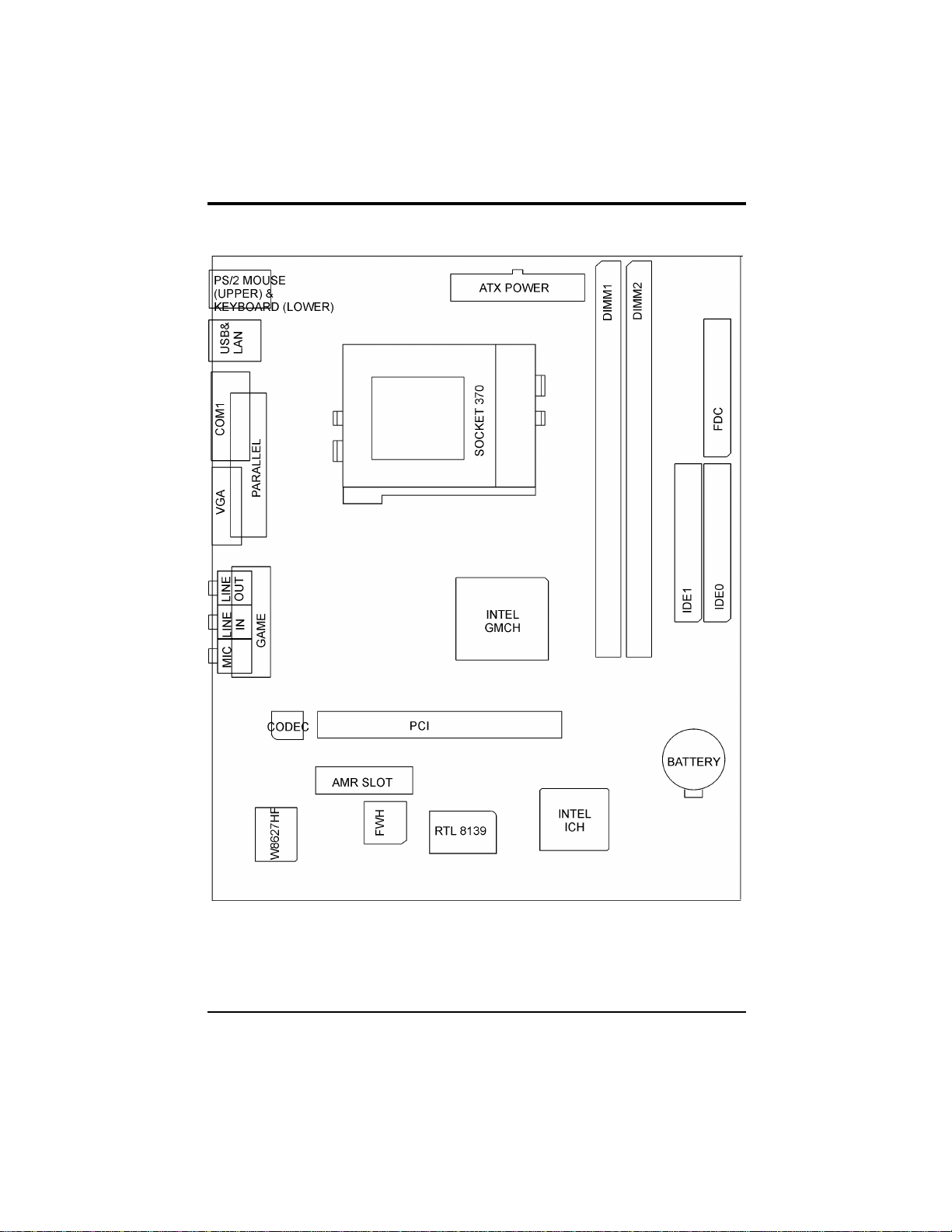
CHAPTER 1 INTRODUCTION 1
CHAPTER 2 JUMPER SETTINGS 5
2.1 JUMPERS PRESENTATION 5
2.2 GRAPHICAL DESCRIPTION OF JUMPER SETTINGS 6
2.3 CPU SPEED 7
2.4 JP9 - CLEAR CMOS DATA 7
2.5 JP12 – BIOS LOCK/UNLOCK SELECT 8
2.6 JP5 – ONBOARD CODEC SETTING 8
2.7 JP10, JP11 – ONBOARD ETHERNET SETTING 8
2.8 MEMORY CONFIGUARTION 9
CHAPTER 3 CONNECTOR CONFIGURATION 11
3.1 U1 – SOCKET370 FOR CELERON CPU 12
3.2 J1 – MULTIPLE FUNCTION JUMPER 12
3.3 J2, J3 J4– CPU FAN CONNECTOR 12
3.4 J5 - ATX POWER SUPPLY CONNECTOR 13
3.5 J6 - FLOPPY DRIVE CONTROLLER 13
3.6 J7, J8 –PRIMARY /SECONDARY IDE CONNECTORS 13
3.7 J12 – CUSTOMER IR CONNECTOR 13
3.8 J16 – CD-ROM AUDIO CONNECTOR (MISUMI/ 14
PANASONIC) 14
3.9 J17 – CD-ROM AUDIO CONNECTOR (SONY) 14
3.10 J13 – USB PORTS & LAN PORT 15
3.11 J21 – VGA CONNECTOR 15
3.12 J22 – PARALLEL PORT CONNECTOR 15
3.13 J23 – SERIAL PORT COM1 15
3.14 J25 – PS/2 MOUSE CONNECTOR 16
3.15 J26 – PS/2 KEYBOARD CONNECTOR 16
3.16 AUDIO PORT CONNECTOR 16
CHAPTER 4 AWARD BIOS 17
CHAPTER 5 DRIVER INSTALLATION 19
5.1 VGA ON BOARD DRIVERS INSTALLATION 19
5.2 IDE DRIVERS INSTALLATION 20
5.3 AUDIO/AC97 ON BOARD DRIVERS INSTALLATION 20
5.4 LAN DRIVERS INSTALLATION 20
CHAPTER 6 FLASH AND DMI UTILITY 21
6.1 AWARD FLASH UTILITY 21
6.2 DESKTOP MANAGEMENT INTERFACE (DMI) OVERVIEW 23
APPENDIX QUICK GUIDE 27


1
CHAPTER 1 INTRODUCTION
Preface
The motherboard is a 4 layers, FlexATX form factor high performance PCI mainboard. It
includes Intel 810 system chipset, Winbond W83627HF LPC I/O controller and Realtech
RTL8139A Ethernet Controller.
Features
•Intel® Accelerated Hub Architecture Increased I/O performance allows better
concurrency for richer multimedia applications.
•Integrated graphics/AC97 controller BOM cost savings, more flexibility and better audio
quality.
•Intel® 3D graphics with Direct AGP Vivid 2D and 3D graphics, BOM cost savings,
efficient use of system memory for graphics, O/S and applications
•Optional 4MB of dedicated display cache video memory enables SKU differentiation
with increased 3D graphics performance improvement over Direct AGP.
•Low-power sleep modes Energy Savings, Suspend to DRAM (3 Watts), and On Now in
10 seconds approx..
•One software driver code base more stable platform, higher quality graphics, reduced
OEM support costs.
•Intel® Random Number Generator (RNG) enables ISV's to strengthen security products.
•Soft DVD MPEG 2 playback with Hardware Motion Compensation Life-like video and
audio.
•100MHz System Bus capable Flexibility for performance headroom.
•2 USB ports Plug and Play.
•10/100M BPS Ethernet Controller on board supported (optional).
Processor
•Intel PPGA S370 series.
•The mainboard can run with following speeds:
300A, 333, 366, 400, 433, 466, 500 or 533MHz
•Jumperless CPU HOST frequency

Chapter 1
2
Chipset
•Intel 810 chipsets
•Winbond W83627HF LPC I/O Controller
•Realtech RTL8139A Ethernet Controller
Main Memory
•Memory configurations up to 512MB SDRAM
•DIMM socket for SDRAM (3.3V unbuffered).
•Support both Synchronous DRAM and Extended Data Output (EDO) Mode DRAM
Modules.
•ECC Function ensures data correction and integrity.
Multi I/O
•On board Multi-I/O supports two serial, one parallel ports and floppy drive controller.
•Serial ports are 16550 Fast UART compatible.
•Parallel port has EPP and ECP capabilities.
•PS/2 keyboard and PS/2 mouse connector is provided.
•Keyboard /mouse wake-up by programmable buttons.
•Programmable AC Power Failure Recovery.
•IrDA/FIR supported.
•USB supported.
PCI IDE
•On board supports PCI Master IDE Controller, two connectors support up to four IDE
devices such as HDD, CD ROM drive and Tape Back-up drives, etc.
•PCI Master IDE controller supports PIO Mode 3 and 4 devices, I/O data transfer rate can
be up to 16.6MB/s.
•Ultra DMA Mode supported. Transfer rate can be up to 66MB/s.
Ethernet Controller
•10/100MHz PCI Ethernet controller on board.
System BIOS
•Award BIOS (4M FWH).
Slots
•One PCI slot
•One AMR slot
Form Factor
•Flex ATX Form Factor Size (229mm x 191mm) 4 Layers

Introduction
3
Fig. 1 Key Components of the Mainboard

Chapter 1
4

5
CHAPTER 2 JUMPER SETTINGS
2.1 JUMPERS PRESENTATION
Pins 1 and 2 are shorted with a jumper cap.
1 2 3
Pins 2 and 3 are shorted with a jumper cap.
1 2 3
The jumper is shorted when the jumper cap is placed
over the two pins of the jumper.
The jumper is open when the jumper cap is removed
from jumper.

Chapter 2
6
2.2 GRAPHICAL DESCRIPTION OF JUMPER
SETTINGS
Fig. 2 Jumper Location of the mainboard

Jumper Settings
7
2.3 CPU SPEED
The table below summaries the CPU frequency and settings of each jumper of the
motherboard.
CPU Type Freq. Bus Freq. Bus Ratio
300MHz 4.5x
333MHz 5.0x
366MHz 5.5x
400MHz 6.0x
433MHz 6.5x
466MHz 7.0x
500MHz 7.5x
PPGA S370 Celeron
533MHz
66MHz
8.0x
Table 1
2.4 JP9 - CLEAR CMOS DATA
JP9 is used to clear the content of the CMOS Data in the RTC (build in PIIX4
chip).
JP9 Description
1Normal
1Clear CMOS Data
Table 2 Clear CMOS Data

Chapter 2
8
2.5 JP12 – BIOS LOCK/UNLOCK SELECT
JP12 Description
Unlock(Default)
Lock
Table 3
2.6 JP5 – ONBOARD CODEC SETTING
JP5 Description
1 Enabled
1Disabled
Table 4
2.7 JP10, JP11 – ONBOARD ETHERNET SETTING
JP10,JP11 Description
Enabled
Disabled
Table 5

Jumper Settings
9
2.8 MEMORY CONFIGUARTION
The mainboard lets user upgrade system memory via DIMM sockets on the
mainboard. On board memory is located in four banks: Bank 0 - 3. Two DIMM
sockets are provided for EDO DRAM or Synchronous DRAM. Table 6 provides
the typical memory configurations supported by the mainboard.
Bank 0/1 (DIMM1) Bank 2/3 (DIMM2)
Installed None
None Installed
Installed Installed
Table 6
The maximum memory size is up to 512MB (SDRAM). The size of each DIMM
can be 32MB, 64MB, 128MB, 256MB and 512MB.

Chapter 2
10

11
CHAPTER 3 CONNECTOR
CONFIGURATION
Once the mainboard has been fastened into system case, the next step is to connect the
internal cables. The internal cables are wire leads with plastic female connectors that attach
to the connectors. The mainboard connectors have varying numbers of pins and are the
points of contact between the mainboard and other parts of the computer.
Fig 3 Connector Location

Chapter 3
12
3.1 U1 – SOCKET370 FOR CELERON CPU
U1 is the Socket370 for Celeron CPU.
Fig. 4 Socket370 for Celeron CPU
3.2 J1 – MULTIPLE FUNCTION JUMPER
J1 is a front panel multi-function jumper includes speaker, reset, keylock, harddisk,
LED, GREEN LED and power button (suspend switch). The pin definition is
following figure.
Fig. 5 Multiple Function Jumper
3.3 J2, J3 J4– CPU FAN CONNECTOR
J2, J3, J4 are three-pin connectors, which are used to connect with the CPU Fan
or the Case Fan which will be monitored by the on board hardware doctor, and
controlled the Fan speed.

Connector Configuration
13
3.4 J5 - ATX POWER SUPPLY CONNECTOR
J5 is a 2x10 pin male connector. Plug the power connector of the ATX power
supply into the connector.
Fig. 6 ATX Power Supply Connector
3.5 J6 - FLOPPY DRIVE CONTROLLER
This connector supports the floppy drive ribbon cable. After connecting the single
end to the board, connect the two plugs on the other end to the floppy drive.
3.6 J7, J8 –PRIMARY /SECONDARY IDE
CONNECTORS
These connectors support the provided IDE hard disk ribbon cable. After
connecting the single end to the board, connect the two plugs on the other end to
your hard disk or other device.
3.7 J12 – CUSTOMER IR CONNECTOR
J12 is a ten-pin connector for the IrDA/ASKIR/Customer Infrared device. The pin
definition is listed as following:

Chapter 3
14
Fig. 7 Customer IR Connector
3.8 J16 – CD-ROM AUDIO CONNECTOR (MISUMI/
PANASONIC)
J16 is a four-pin connector, which is used to connect with the Panasonic or Misumi
CD-ROM audio output. The pin definition is as following:
Fig. 8 CD-ROM Audio Connector
3.9 J17 – CD-ROM AUDIO CONNECTOR (SONY)
J17 is a four-pin connector, which is used to connect with the Sony CD-ROM audio
output. This pin definition is as following:
Fig. 9 CD-ROM Audio Connector
This manual suits for next models
1
Table of contents
Other DTK Motherboard manuals