FLY DS 110 User manual

DS 110 Service Menu
Version number: V1.0
Draft Ren Mingwei
Auditing Li Xilin
Authorize ZhaoGang
Date 2010-6-18
Shenzhen IFLY Communication Technology Co., Ltd.

Contents
1 Overview DS 110....................................................................................................................1
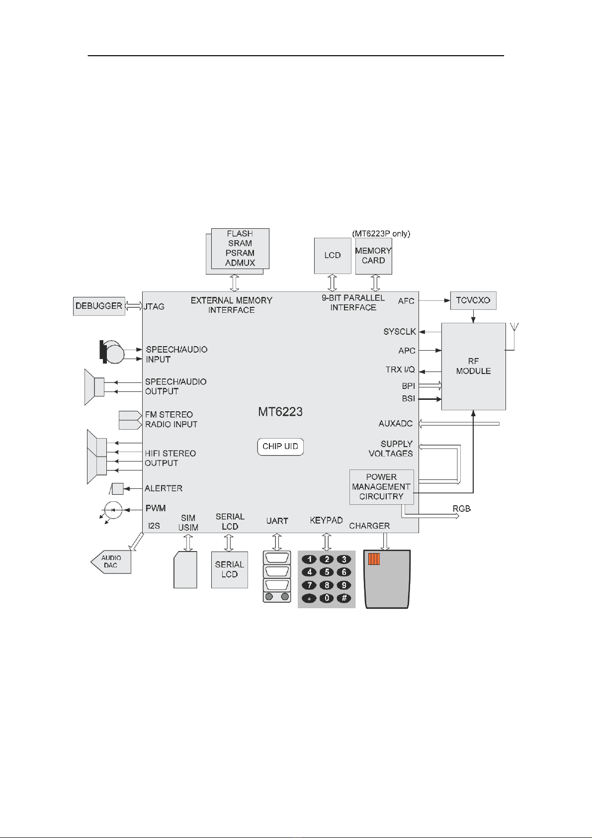
1.1 About DS 110 Phone........................................................................................................1
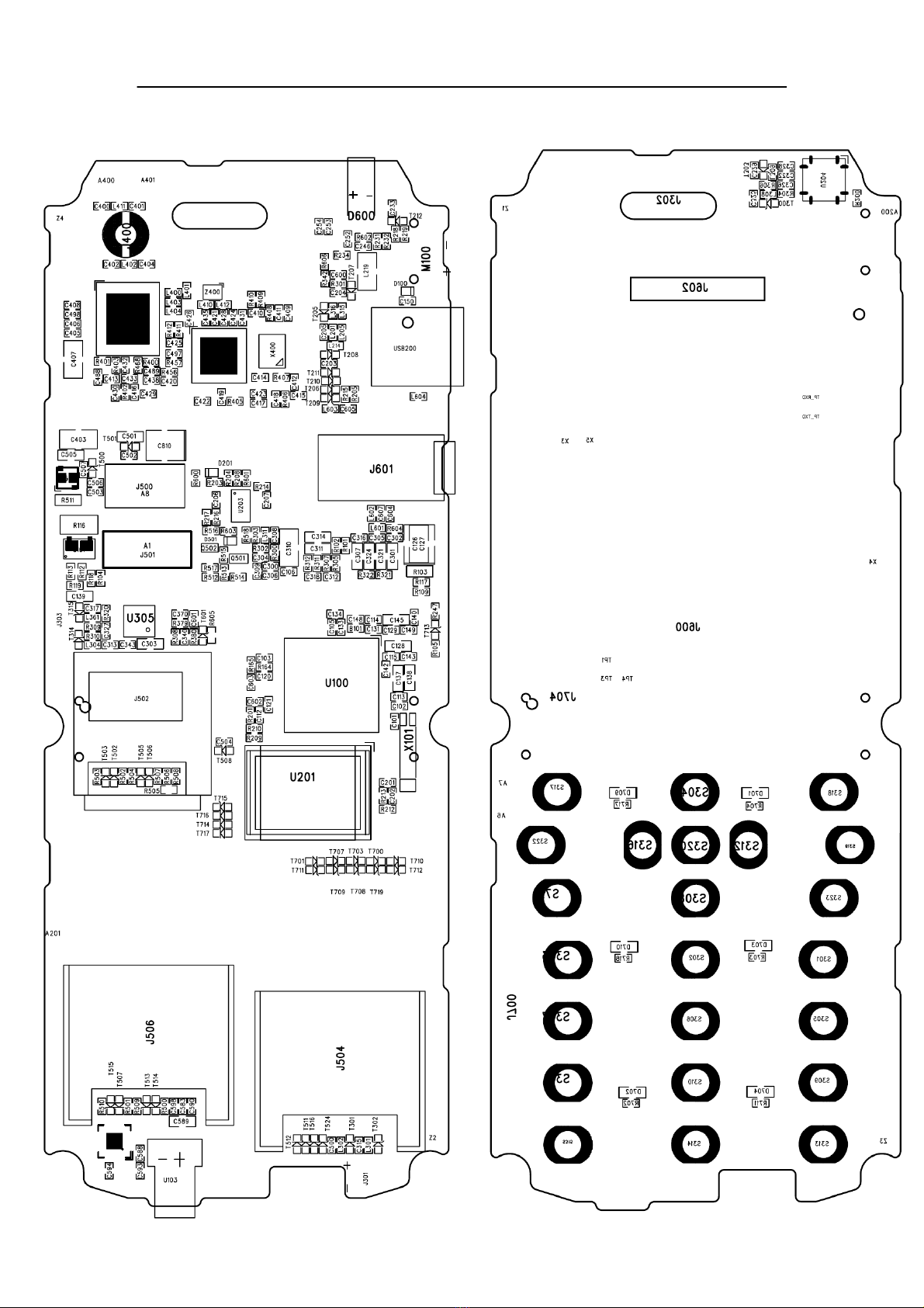
1.2 Distribution of the mainboard components.......................................................................2
2 RF...........................................................................................................................................3
2.1 RF Overview.....................................................................................................................3
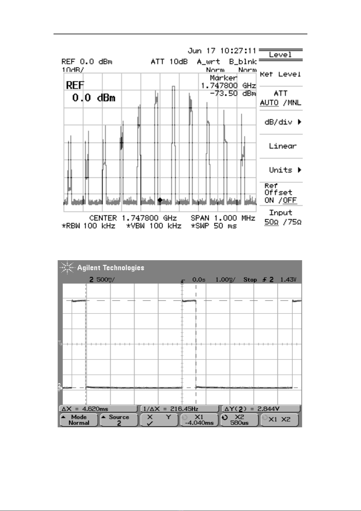
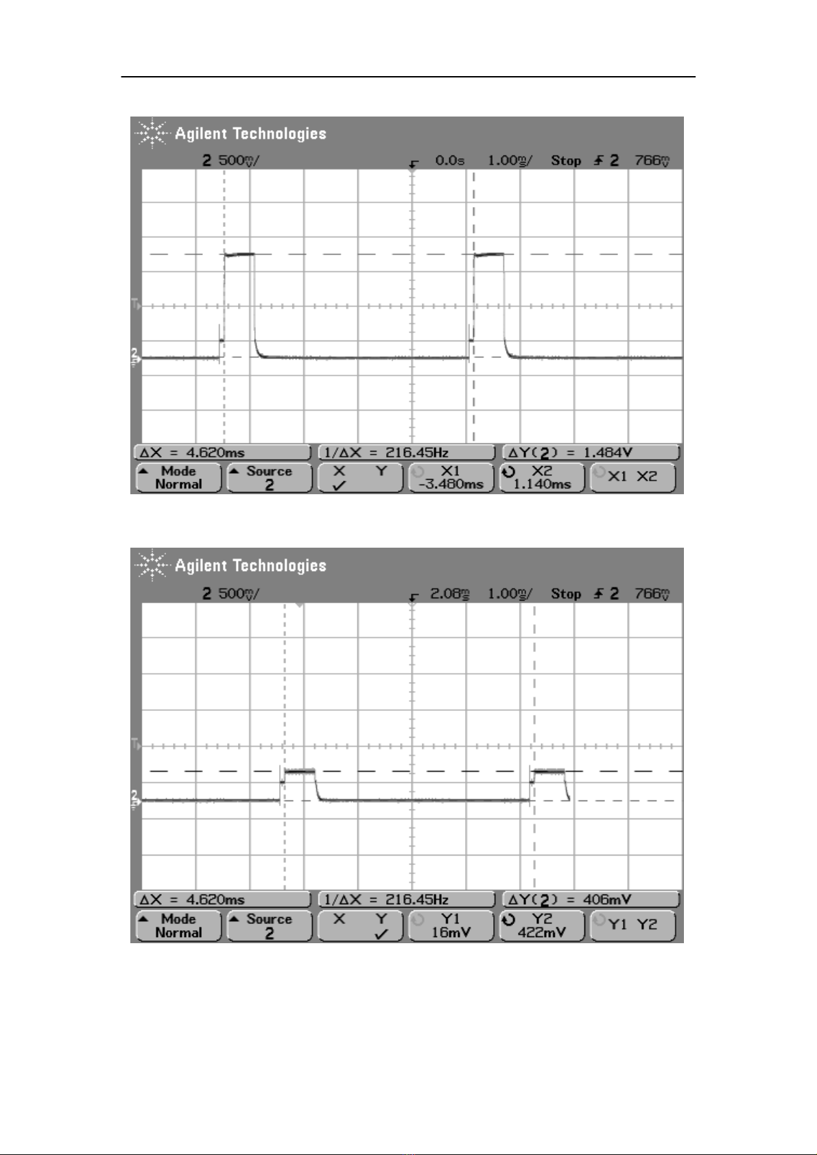
2.2 Transmit ............................................................................................................................3
2.3 Receive..............................................................................................................................3
2.4 Common RF Malfunction................................................................................................4
3 Baseband................................................................................................................................15
3.1 Baseband Overview ..........................................................................................................15
3.2 Logic.................................................................................................................................15
3.3 Power management...........................................................................................................15
3.4 Audio Frequency...............................................................................................................16
3.5 Baseband common malfunction........................................................................................17
4 Reference for maintenance...................................................................................................21
4.1 No Signal ..........................................................................................................................21
4.2 Phone does not “power on”...............................................................................................21
4.3 LCD trouble ......................................................................................................................21
4.4 Sound trouble....................................................................................................................21
4.5 Keyboard malfunction.......................................................................................................21
5 Tools.........................................................................................................................................22
5.1 Downloading Operation Manual...................................................................................22
5.2 Repair tools Operation Manual......................................................................................22
5.3 write SN Operation Manual...........................................................................................22
5.4 Calibration Operation Manual.......................................................................................22
5.5 Testing Operation Manual .............................................................................................22
5.6 Function testing Operation Manual...............................................................................22
5.7 Detailed maintenance program .....................................................................................22

DS 110 Service menu
1 Overview DS 110
1.1 About DS 110 Phone
DS 110 mainboard is based on the MTK platform designed to support
dual-band which supporting the FM, the mainboard system consists of the base-
band (CPUMT6223D+EN71PL03280-70CWP)and the RF
(AD6548+PARPF88143B).
1

DS 110 Service menu
1.2 Distribution of the mainboard components
2

DS 110 Service menu
2 RF
2.1 RF Overview
RF part mainly consists of transceiver AD6548 (adopts program of near-zero IF receiver,
supporting the EGSM / DCS and 26M Crystal as the clock input, integrated clock buffer, LO
VCO and TX VCO and regulator, only need for external connections of VBAT / AVDD),
PARPF88143B (it supports EGSM / DCS and integrated automatic power control and
transceiver switch).
AD6548 Baseband Chip
GSM RF and BB interface diagram
Transceiver (AD6548) with the RF modulation and demodulation functions contains IF
frequency synthesizer and VCO RF, which is part of the core component of the RF. PAhas a
major role in amplification of modulation signal, and it must be controllable and the
speed should meet the GSM agreement.
2.2 Transmit
TX is composed of the modulation loop, power amplifier and antenna switch. PLL is
mainly in the internal AD6548, I / Q signal first enters into the AD6548, after entering the
PLL the signal is modulated to RF, and then it outputs from the chip to PA, converts into
electromagnetic energy through antenna by the antenna switch after enlarged.
PA:
This part adopts voltage control to achieve and its role is to amplify the signal power in
accordance with the requirements. It is divided to two different power levels through
VRAMP signal. The transmit signal of GSM is 5 to 19, power is from 3.2MW to 2W while
DCS is 0 ~ 15, power from 1MW ~ 1W. PA is time-sharing work controlled by TX-EN chip,
the output power of PA is controlled by VRAMP (APC) through the
voltage. PA is intermittent work, by the BS to achieve the choice of frequency bands.
2.3 Receive
Antenna RX – AD6548 (RX_VCO mixer) - band-pass - Amplification - filter - Amplification -
RX_VCO mixer - CPU
3

DS 110 Service menu
2.4 Common RF Malfunction
2.4.1 Detection and Maintenance Flow Chart of MS Transmit
malfunction
(No transmit) Connect PC and cell
phone with maintenance of line, use the
Repair software making mobile phone
access to transmit state.
Check IQ signal input
pin of Transceiver,
whether there is
IQ signal?
N Check CPU
Y
Check RF signal output
pin, whether there is
any RF
YN
Check antenna
switch or matching
network
CheckTransceiver,whethe
there is any RF output signal?
Y
VBAT, PA_EN, N
BANDSW_DCS,V
APC, are they OK?
Check
Transceiver
YExternal
N Y
Replace PA
Check CPU
Replace
Transceiver
2.4.2 The maintenance process of Transmit malfunction
Use the Repair software making mobile phone access to transmit state. Choose 62CH in
GSM band, POWER Level for 5, DCS for 700CH, POWER Level for 0. Then, first observe
whether the current rises, and use the spectrum analyzer and oscilloscope to observe the
signal given in the above-mentioned flow chart, the specific signal waveforms shown as
below:
4

DS 110 Service menu
IQ signal waveforms of transceiver in transmit state:
IQ
RF interface spectrum analyzer is as follows:
GSM transmit signal
5

DS 110 Service menu
DCS transmit signal
PA-EN waveforms of PA in transmit state:
PA-EN
6

DS 110 Service menu
PA. BAND-SW waveforms:
PA.BAND-SW
(GSM)
PA.BAND-SW
(DCS)
7

DS 110 Service menu
PA Vramp waveforms:
Vramp (pcl5)
Vramp (pcl 19)
8

DS 110 Service menu
2.4.3 Detection and Maintenance Flow Chart of MS Receive
malfunction
NoReceive
Open Repair Software to connect PC with mobile phone, make the
phone access to receiving state, adjust signal generator to
corresponding CH, and connect the signal line to phone’s RX_SW.
Check MT6223D
Y Check IQ signal output pin
of Transceiver,
whether there is IQ signal?
N
Check Transceiver input pin,
whether there is any input
Y signal? N
N
Check CPU
Are Transceiver
SDATA 、SCLK 、
LE、RFVCOEN all
correct?
Y
N
Check or replace the
antenna switch and
matching circuits
Whether PA signal
input pin has
received any signal?
Y
Whether the voltage
Transceiver used is
normal? Is 26MHz
normal?
Check RX-filter
N
Check the
corresponding
power supply
and circuits of
26MHZ
Y
Replace
Check Transceiver
External RC components
. Transceiver
2.4.4 The maintenance process of Receive malfunction
Maintenance process of NO Receive: Use Repair software to make mobile phone access
to pure receive state →Choose 62CH, Rx Mode CH62=947.4MHZ, Input power:-
60dbm in GSM frequency bands →Choose 698CH, Rx Mode
CH698=1842.4MHZ, Input power:-60dbm in DCS frequency bands →Adjust signal
generator to corresponding CH, connect the signal line to Cable of RF →Measure
the related key signal by using Spectrum analyzer and Oscilloscope →Measure the
signal output pin of Transceiver, whether there is any correct IQ signal output to CPU
→Y: Check CPU (MT6223D) / N: Check Transceiver input pin, whether there is any
corresponding CH input signal (Y: Check whether Transceiver has correctly
controlled the signal →Check whether the
9

DS 110 Service menu
voltage supply is normal →if normal, Transceiver can be judged of damaged / N: Check
PA and the paths ahead )
Signal waveforms refer to the following:
Output signal of Signal generator (Input):
GSM CH62 channel receives the signal
DCS CH 698 channel receives the signal
10

DS 110 Service menu
IQ signal output pin of Transceiver the state of receiving IQ signal:
The signal Transceiver received from CPU used to access the internal
register of
Transceiver. The corresponding waveform is as follows:
IQ Signal
Frequency-s
ynthesizing
signal
11

DS 110 Service menu
3W(SDATA)
3W(SCLK)
12

DS 110 Service menu
3W(LE)
26M clock (can be measured by using the ACCoupling)
The AFC (automatic frequency control) from CPU to the crystal oscillator makes crystal
oscillator output accurate 26MHZ to Transceiver.
26M Output
26M
Input
13

DS 110 Service menu
VAFC
TCXO output(26MHZ)
14

DS 110 Service menu
3 Baseband
3.1 Baseband Overview
DS 110 Baseband consists of CPUMT6223D and Program Memory. UMT6223D baseband,
the core device of the mainboard, is responsible for the normal work among various parts
of mainboard, such as voice processing, image processing, power management as well
as MS communications.
UMT6223D digital baseband contains 32-bit ARM7E core. UMT6223D which is an
enhanced GSM Processor integrated Channel Codec subsystems interiorly including
Channel Codec, Intertlace / Deinterleave, Encryption / Decryption and Control Processor
subsystems including ARM7EJS and its peripheral circuits. There are 26
address lines,16 data lines, 4 chip select lines, provided 6 external interrupt Interface,
26M/52M operation clock.
Analog baseband contains UMT6223D analog baseband chip, audio, baseband codec and
power management. Four major functional blocks integrated internal:
Audio codec including Voice input / Output channel, Buzzer output;
Baseband codec including Differential I, Q input / output, GMSK modulation and A / D,
D / A; Auxiliary parts including AFC DAC, RAMP DAC, AGC DAC and a seven-channel A /
D. And WATCHDOG interface is set internal to enhance the stability of the system.
3.2 Logic
Logic part is composed of MTK base-band management chip
UMT6223D, power management chip MT6223D and Nor flash.
UMT6223D:CPU
NOR Flash:
MT6223D:PMU
3.3 Power management
Power management consists of the charging circuit integrated in MT6223D and the external
charging circuit. It provides 7 road LDO voltage. Besides, it completes the logic level
conversion of SIM card. The chip also outputs the system reset signal.
15

DS 110 Service menu
Boot process:
The normal boot is to press boot key which is that the PWRKEY is being dragged down.
Once the boot key is pressed, all LDO are open except VSIM. After VCORE
opening RESET timer and timer out, RESET is being pitched up to start the digital
baseband chip, that is, UMT6223D starts to run and roll polling its ROWX pin, pitch up its
PWRONIN pin, then you can release the boot key. This is the initial boot process.
3.4 Audio Frequency
The sound quality performs more pleasant on account of audio processing integrated in
UMT6223D
3.4.1 Speaker loop
3.4.2 MIC loop
Check basic bias voltage signal of MICBIASP and MICBIASN and the language signal of
MIC itself when the MIC is good but no response of LOOP MIC in test.
16

DS 110 Service menu
3.4.3 Earphone loop
Earphone loop includes headset speaker and MIC two-way signal. Check the
circuit access situation when there is something abnormal (such as: no sound in
headset speaker, Mic invalid, etc.) after inserting the earphone while the headset
accessories are good.
3.5 Baseband common malfunction
3.5.1 Nor flash programming does not download
Data lines used for downloading software: VBAT, TX, RX, GND, CHARGE. It is mostly due
to the false solder and wire bonding. First check whether the serial port of PC and cell
phone is unrestricted, if not, it is caused by being lack of devices or empty solder of power
manager, USB-con and peripheral resistance. Measure the TX, RX signals by
using AC-coupled oscilloscope to track the signal flow, if a certain period circuit of no
signal it may be AC short circuit to ground, or is caused by a short circuit and open
circuit. On checking the malfunctions, first should carefully observed the welding of
these devices with a magnifying glass, then plug in the download line to observe whether
the current is normal, there is short-circuit to ground of VCHG or VBAT if the current is
large, at this time
17

DS 110 Service menu
cut off power supply as soon as possible, and then find the short-circuit point. It may be
the abnormal output power supply of a certain circuit that the current is larger than normal
(about 30 mA) but not particularly large, at this time should check whethe the valgate of
VCORE (1.8V), VDD (2.8V), VADD (2.8 V), VTCXO (2.8V), VRTC (1.5V), VMEM (2.8V) is
noamal, if not, bad welding can be detected. Focus on checking the welding of PMU and
USB-CON if there is a little or no current. Unplug and re-plug the download line to see if it
is caused by poor contact; It can test that whether the output of 26MHz clock signal to the
CPU is normal by using oscilloscope.
3.5.2 Detection and Maintenance Flow Chart of No download
malfunction
Not download
Eliminate any
reasons for not
download except
the cell phone.
Yes
Check whether it is the problems
of allocation of procedure,
download cable, power supply,
software, PC phone.
Check whether
the5pin
connector USB-CON
is falsesoldered
or damaged.
NO
NO Check whether the serial port of
PC and cell phone is unrestricted.
NO
Check USB-
con peripheral
resistance
Yes
Connect the download line
and observe the ammeter whether
the current is high (normal current
is generally about 30mA).
Yes
Quickly disconnect
the connection, and
touch the chip gently to
see if it is hot, if not,
focus on measuring
the short-circuit
point by using
multimeter.
Alittle or no current
Normal current but no download
Check whether the voltage supply of CPU
power manager, PMU and LDO is normal,
whether there is any power supply open circuit.
Check VCOR 、VDD 、VADD
VTCXO 、VRTC 、VMEM 、measure the
clock signals of 26MHZ、32KHZ
Check whether CUP and NORFLASH
is OK, LDO is normal?
18
Table of contents
Other FLY Cell Phone manuals