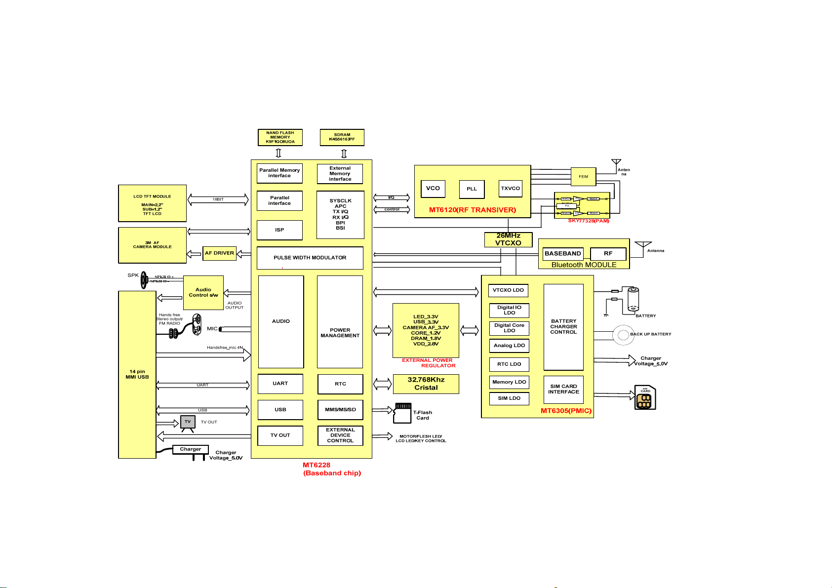
1.2 Functional Description
1.2.1 Receiver
The receiver section of MT6120 includes Tri-band low noise amplifiers (LNAs), RF
quadrature mixers, an on-chip channel filter, Programmable Gain Amplifiers (PGAs),
quadrature second mixers, and a final low-pass filter. The very low-IF MT6120 uses
image-rejection mixers and filters to eliminate interference. With accurate RF
quadrature signal generation and mixer matching techniques, the image rejection of the
MT6120 can reach 35 dB for all bands. The fully integrated channel filters rejects
interference, blocking signals, and images without any external components Compared
to a direct conversion receiver (DCR), MT6120’s very low-IF architecture improves
the blocking rejection, AM suppression, as well as the adjacent channel interference
performance. Moreover, the very low-IF architecture eliminates the need for
complicated DC offset calibration that is necessary in a DCR architecture. In addition,
the common-mode balance requirement of the SAW filter input is relaxed. The
MT6120 provides the analog IQ baseband output without any extra frequency
conversion components.
The MT6120 includes Three differential LNAs for GSM 850 (869 MHz – 893 MHz),
DCS 1800 (1805 MHz-1880 MHz) and PCS 1900 (1930 MHz –1990 MHz). The
differential inputs are matched to 200 Ω SAW filters using LC networks. The gain of
the LNAs can be controlled either high or low for an additional 35 dB dynamic range
control. Following the LNAs are the image-rejection quadrature RF mixers that down-
convert the RF signal to the IF frequency. No external components are needed at the
output of the RF mixers.
The IF signal is then filtered and amplified through an image-rejection filter and a PGA.
The multi-stage PGA is implemented between filtering stages to control the gain of the
receiver. With 2 dB gain steps, a 78 dB dynamic range of the PGA ensures a proper
signal level for demodulation. The quadrature 2nd mixers are provided on-chip to
down convert IF signal to baseband in an analog differential IQ format.
1.2.2 Transmitter
The MT6120 transmitter section consists of two on-chip TX VCOs, buffer amplifiers, a
down-converting mixer, a quadrature modulator, an analog phase detector (PD) and a
digital phase frequency detector (PFD), each with a charge pump output and on chip
loop filter. The dividers and loop filters are used to achieve the desired IF frequency
from the down-conversion mixer and quadrature modulator. For a given transmission
channel, the transmitter will select one of the two different TX reference dividing
numbers. These built-in components, along with an internal voltage controlled
oscillator (TX VCO) and a loop filter, implement a translation loop modulator. The TX
VCO output is fed to the power amplifier (PA). A control loop, implemented externally,
is used to control the PA’s output power level.
1.2.3 TX VCO
Two power VCOs are integrated with OPLL to form a complete transmitter circuit. The
TX VCO output power is typically 9 dBm with +/- 2.5dB variation /
GSM850 bands and +8 dBm output power with +/- 2dB variation in DCS1800/