2 FPGA Offline Programmer Instructions
2FPGA Offline Programmer Instructions
2.1 Overview
Offline programmer is a device that offline programs GW1N(R) chips.
It has the features of data confidentiality, portability, multi-path
programming, etc. It is suitable for rapidly large-volume production at the
factory and is convenient for maintenance personnel to carry out. The
offline programmer can simultaneously program four FPGA devices, and
automatically detect device access and program in a single interface,
which greatly increases the mass production rate.
The offline programmer encrypts and saves the data using an
AES-128 advanced encryption algorithm, and the key is saved after
several times of encrypting. AES is a set of internationally recognized,
commonly used and secure encryption standards that ensure securely
delivering data.
2.2 Offline Programmer Instructions
The offline programmer can be configured and managed using the
offline programmer software, such as data stream file management, upper
burner count management, and writer firmware upgrade. The software
supports Windows 7 and above operating systems. After configuration, the
offline programmer can be connected to the FPGA to program.
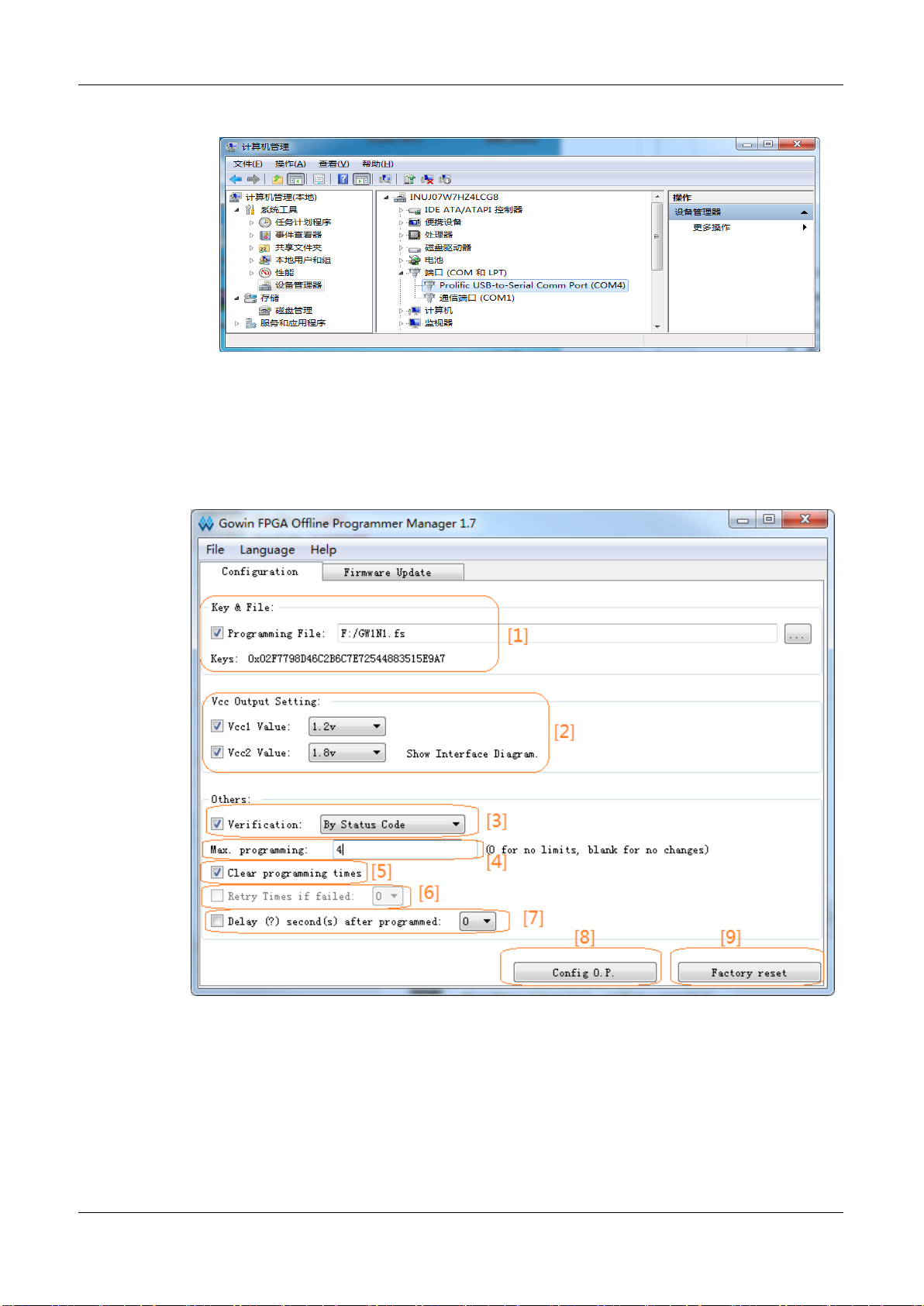
2.2.1 Software Download and Driver Installation
The relevant software and driver package can be downloaded at
Gowin website or contact the sales for help. Install the driver and the path
is https://www.gowinsemi.com/en/support/devkits_detail/7/. After
installation, use USB cable to connect the programmer and computer, and
USB Serial Port(COMxx) appears on the port, that is, the driver is installed
successfully, as shown in Figure 2-1.